EP4535666A1 - Circuit de remise à zéro à la mise sous tension - Google Patents
Circuit de remise à zéro à la mise sous tension Download PDFInfo
- Publication number
- EP4535666A1 EP4535666A1 EP24203256.3A EP24203256A EP4535666A1 EP 4535666 A1 EP4535666 A1 EP 4535666A1 EP 24203256 A EP24203256 A EP 24203256A EP 4535666 A1 EP4535666 A1 EP 4535666A1
- Authority
- EP
- European Patent Office
- Prior art keywords
- supply voltage
- trip
- voltage
- circuit
- terminal
- Prior art date
- Legal status (The legal status is an assumption and is not a legal conclusion. Google has not performed a legal analysis and makes no representation as to the accuracy of the status listed.)
- Pending
Links
Images


Classifications
-
- H—ELECTRICITY
- H03—ELECTRONIC CIRCUITRY
- H03K—PULSE TECHNIQUE
- H03K17/00—Electronic switching or gating, i.e. not by contact-making and –breaking
- H03K17/22—Modifications for ensuring a predetermined initial state when the supply voltage has been applied
- H03K17/223—Modifications for ensuring a predetermined initial state when the supply voltage has been applied in field-effect transistor switches
-
- G—PHYSICS
- G01—MEASURING; TESTING
- G01R—MEASURING ELECTRIC VARIABLES; MEASURING MAGNETIC VARIABLES
- G01R19/00—Arrangements for measuring currents or voltages or for indicating presence or sign thereof
- G01R19/165—Indicating that current or voltage is either above or below a predetermined value or within or outside a predetermined range of values
- G01R19/16533—Indicating that current or voltage is either above or below a predetermined value or within or outside a predetermined range of values characterised by the application
- G01R19/16538—Indicating that current or voltage is either above or below a predetermined value or within or outside a predetermined range of values characterised by the application in AC or DC supplies
- G01R19/16552—Indicating that current or voltage is either above or below a predetermined value or within or outside a predetermined range of values characterised by the application in AC or DC supplies in I.C. power supplies
Definitions
- Integrated circuits include various functional circuits that are critical for operations thereof. Such functional circuits require a supply voltage to be above a predefined value to ensure the accurate execution of associated operations. Such a predefined value of the supply voltage is referred to as a trip value.
- a predefined value of the supply voltage is referred to as a trip value.
- a reset signal generated by a power-on reset (POR) circuit, is utilized to indicate that a supply voltage is above a trip value.
- the reset signal is de-asserted (e.g., is at a logic low state) when the supply voltage is less than the trip value, and when the supply voltage exceeds the trip value, the reset signal transitions from the de-asserted state to an asserted state (e.g., a logic high state).
- the reset signal transitions to the de-asserted state when the supply voltage falls below the trip value.
- the trip values during the ramp-up and the ramp-down may be different.
- the trip node voltage and the reference voltage follow the supply voltage, and are less than the supply voltage.
- the first and second trip detector circuits are deactivated (e.g., are not triggered).
- the reset signal and the control signal are de-asserted.
- the control circuit is deactivated (e.g., is not triggered).
- the reset signal remains de-asserted while the trip node voltage is less than a first threshold value, and transitions from the de-asserted state to the asserted state when the trip node voltage exceeds the first threshold value (e.g., when the supply voltage exceeds a trip-high value).
- the power supply 102 may be configured to generate a supply voltage VDD.
- the supply voltage VDD is equal to 1.8 volts (V).
- the supply voltage VDD may have other values in other embodiments.
- assert is used to mean placing a signal in an active state. Some signals may be assert-high signals whereas some signals may be assert-low signals. With assert-high signals, the assertion of a signal corresponds to the signal being in a logic high state. Conversely, with assert-low signals, the assertion of a signal corresponds to the signal being in a logic low state.
- the reset signal RST is an assert-high signal (e.g., the active state corresponds to a logic high state).
- the trip-high and trip-low values do not vary significantly across different ramp rates of the supply voltage VDD.
- the trip-high value is greater than the trip-low value.
- the trip-high value may be equal to 0.9 V and the trip-low value may be equal to 0.7 V.
- the trip-high value and the trip-low value may be different in other embodiments.
- the trigger points e.g., the trip-high value and the trip-low value
- all the voltages and signals of the POR circuit 104 are equal to the supply voltage VDD or a ground voltage, during the steady state of the supply voltage VDD.
- the consumption of non-zero steady-state (e.g., quiescent) currents by the POR circuit 104 is prevented.
- the current consumption of the POR circuit 104 is null.
- the POR circuit 104 is thus capable of detecting both the ramp-up and ramp-down trigger scenarios, whilst avoiding consumption of non-zero steady-state currents, which renders the POR circuit 104 highly efficient and accurate as compared to some conventional POR circuits.
- the POR circuit 104 is explained in detail in conjunction with FIGS. 2 and 3 .
- the functional circuit 106 is one exemplary functional circuit that may utilize the reset signal RST for its operation.
- the scope of the present disclosure is however not limited to it.
- the reset signal RST may be utilized by various other functional circuits of the IC 100, without deviating from the scope of the present disclosure.
- FIG. 1 illustrates that all the circuits are implemented on the IC 100, the scope of the present disclosure is not limited to it. In various other embodiments, some circuits may be external to the IC 100. For example, in some embodiments, the power supply 102 may be external to the IC 100.
- a voltage of the low supply voltage terminal may correspond to a non-zero value (e.g., -1 V, 1 V, or the like).
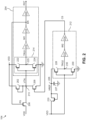
- FIG. 2 illustrates a schematic circuit diagram of the POR circuit 104 in accordance with an embodiment of the present disclosure.
- the POR circuit 104 may include a first diode circuit 202, a first trip detector circuit 204, a first control transistor 206, a second control transistor 208, a second diode circuit 210, and a second trip detector circuit 212.
- the first diode circuit 202 may be coupled to the power supply 102 and the first trip detector circuit 204.
- Examples of the first diode circuit 202 may include a diode, a diode-connected transistor, or the like.
- the first diode circuit 202 is a diode-connected transistor.
- the first diode circuit 202 is referred to as a "first diode-connected transistor 202".
- the first diode circuit 202 may be implemented with a diode or other type of diode circuit (not shown).
- the first diode-connected transistor 202 corresponds to a p-channel metal-oxide-semiconductor (PMOS) transistor.
- PMOS metal-oxide-semiconductor
- the first diode-connected transistor 202 may include first and second current terminals and a control terminal.
- the first and second current terminals of a transistor correspond to source and drain terminals of the transistor, respectively, and the control terminal corresponds to a gate terminal of the transistor.
- the source terminal of the first diode-connected transistor 202 may be coupled to the power supply 102, and may be configured to receive the supply voltage VDD from the power supply 102.
- the drain terminal of the first diode-connected transistor 202 may be coupled to the gate terminal thereof, thereby resulting in a diode-connected transistor configuration.
- the source terminal of the first diode-connected transistor 202 may correspond to a first terminal of the first diode circuit 202
- the drain and gate terminals of the first diode-connected transistor 202 may correspond to a second terminal of the first diode circuit 202.
- the drain terminal of the first diode-connected transistor 202 may be further coupled to the first trip detector circuit 204, the first control transistor 206, and the second control transistor 208 at a trip node 213. Further, the first diode-connected transistor 202 may be configured to generate a trip node voltage VTN at the drain terminal thereof (e.g., at the trip node 213).
- the trip node voltage VTN ramps up based on the ramp-up of the supply voltage VDD and is a reduced version of the supply voltage VDD (e.g., is less than the supply voltage VDD), until the supply voltage VDD exceeds the trip-high value.
- the trip node voltage VTN is equal to a difference between the supply voltage VDD and a threshold voltage of the first diode-connected transistor 202, until the supply voltage VDD exceeds the trip-high value.
- the trip node voltage VTN is adjusted to be equal to the supply voltage VDD.
- Such control of the trip node voltage VTN is executed by the first control transistor 206.
- the trip node voltage VTN remains equal to the supply voltage VDD until the supply voltage VDD falls below the trip-low value. At such an instance, the trip node voltage VTN may be pulled down to the ground terminal. Such control of the trip node voltage VTN is executed by the second control transistor 208.
- the first trip detector circuit 204 may include an input terminal configured to receive the trip node voltage VTN and an output terminal configured to generate the reset signal RST. Further, the first trip detector circuit 204 may be configured to provide the reset signal RST to the functional circuit 106. To enable the generation of the reset signal RST, the first trip detector circuit 204 includes first through fourth inverters 214-220.
- the first inverter 214 may be coupled to the first diode-connected transistor 202 (e.g., the drain terminal of the first diode-connected transistor 202), the power supply 102, and the ground terminal.
- the first inverter 214 may be configured to receive the supply voltage VDD and the trip node voltage VTN from the power supply 102 and the drain terminal of the first diode-connected transistor 202, respectively, and generate a first trigger signal TRG1 based on the trip node voltage VTN and the supply voltage VDD.
- the first trigger signal TRG1 is an assert-low signal.
- the first inverter 214 includes a high supply terminal configured to receive the supply voltage VDD, a low supply terminal coupled to the ground terminal, an input terminal configured to receive the trip node voltage VTN, and an output terminal configured to generate the first trigger signal TRG1.
- the first inverter 214 may include first and second high-detection transistors 222 and 224.
- the first high-detection transistor 222 corresponds to a PMOS transistor and the second high-detection transistor 224 corresponds to an n-channel metal-oxide-semiconductor (NMOS) transistor.
- NMOS metal-oxide-semiconductor
- Each of the first and second high-detection transistors 222 and 224 includes source, gate, and drain terminals.
- the source and gate terminals of the first high-detection transistor 222 may be coupled to the power supply 102 and the drain terminal of the first diode-connected transistor 202, and may be configured to receive the supply voltage VDD and the trip node voltage VTN from the power supply 102 and the drain terminal of the first diode-connected transistor 202, respectively.
- the source and gate terminals of the second high-detection transistor 224 may be coupled to the ground terminal and the gate terminal of the first high-detection transistor 222, respectively.
- the gate terminal of the second high-detection transistor 224 may be configured to receive the trip node voltage VTN.
- the drain terminal of the first high-detection transistor 222 may be coupled to the drain terminal of the second high-detection transistor 224 at a first output node 225.
- the first output node 225 corresponds to the output terminal of the first inverter 214.
- the first inverter 214 generates the first trigger signal TRG1 at the output terminal thereof.
- the first threshold value e.g., is equivalent to a logical ⁇ 1'
- the first trigger signal TRG1 transitions from the de-asserted state (e.g., the logic high state) to the asserted state (e.g., the logic low state).
- the first threshold value corresponds to a trip voltage of the first inverter 214.
- the trip node voltage VTN is adjusted to be equal to the supply voltage VDD.
- the adjustment of the trip node voltage VTN based on the transition of the first trigger signal TRG1 is explained in detail below.
- the first trigger signal TRG1 remains asserted and the trip node voltage VTN remains equal to the supply voltage VDD.
- the first trigger signal TRG1 transitions from the asserted state to the de-asserted state when the trip node voltage VTN is pulled down to the ground terminal.
- the second inverter 216 may be coupled to the first inverter 214 (e.g., the drain terminals of the first and second high-detection transistors 222 and 224).
- the second inverter 216 may be configured to receive the first trigger signal TRG1 from the first inverter 214 and generate a first intermediate signal IM1 that is an inverted version of the first trigger signal TRG1.
- the first intermediate signal IM1 is thus an assert-high signal.
- the second inverter 216 may include an input terminal that is coupled to the output terminal of the first inverter 214, and an output terminal configured to generate the first intermediate signal IM1.
- the third inverter 218 may be coupled to the second inverter 216, and may be configured to receive the first intermediate signal IM1 from the second inverter 216.
- the third inverter 218 may be further configured to generate an enable signal EN that is an inverted version of the first intermediate signal IM1.
- the third inverter 218 may include an input terminal that is coupled to the output terminal of the second inverter 216, and an output terminal configured to generate the enable signal EN.
- the enable signal EN is thus logically equivalent to the first trigger signal TRG1. Further, the enable signal EN is an assert-low signal.
- the trip node voltage VTN is adjusted to be equal to the supply voltage VDD based on a logic state of the enable signal EN, as explained in detail below.
- the fourth inverter 220 may be coupled to the third inverter 218, and may be configured to receive the enable signal EN from the third inverter 218.
- the fourth inverter 220 may be further configured to generate the reset signal RST, that is an inverted version of the enable signal EN.
- the reset signal RST is an inverted version of the first trigger signal TRG1.
- the reset signal RST is thus an assert-high signal.
- the fourth inverter 220 may include an input terminal that is coupled to the output terminal of the third inverter 218, and an output terminal configured to generate the reset signal RST.
- the trip node voltage VTN follows the supply voltage VDD and is less than the supply voltage VDD.
- the first trigger signal TRG1 is de-asserted (e.g., is at the logic high state) and the reset signal RST is de-asserted (e.g., is at the logic low state).
- the first trigger signal TRG1 transitions from the de-asserted state to the asserted state (e.g., the logic low state), and consequently, the reset signal RST transitions from the de-asserted state to the asserted state (e.g., the logic high state).
- the trip-high value thus corresponds to a value of the supply voltage VDD at which the trip node voltage VTN exceeds the first threshold value.
- the trip node voltage VTN is the reduced version of the supply voltage VDD (e.g., is equal to the difference between the supply voltage VDD and the threshold voltage of the first diode-connected transistor 202), until the trip node voltage VTN exceeds the first threshold value. Further, when the trip node voltage VTN exceeds the first threshold value, the trip node voltage VTN is adjusted to be equal to the supply voltage VDD. Such an adjustment of the trip node voltage VTN prevents the creation of low impedance paths between the supply voltage VDD (e.g., the power supply 102) and the ground terminal in the first trip detector circuit 204.
- the first trip detector circuit 204 (e.g., the third inverter 218) generates the enable signal EN.
- the enable signal EN is de-asserted (e.g., is at the logic high state) when the trip node voltage VTN is less than the first threshold value and transitions from the de-asserted state to the asserted state (e.g., the logic low state) when the trip node voltage VTN exceeds the first threshold value.
- the enable signal EN remains asserted for the remaining part of the ramp-up and during the steady state of the supply voltage VDD. Further, during the ramp-down of the supply voltage VDD, the enable signal EN transitions from the asserted state to the de-asserted state when the trip node voltage VTN is pulled down to the ground terminal.
- the first trip detector circuit 204 may be further configured to provide the enable signal EN to the first control transistor 206.
- the first control transistor 206 corresponds to a PMOS transistor.
- the first control transistor 206 may include source, gate, and drain terminals. The source and gate terminals of the first control transistor 206 may be coupled to the power supply 102 and the first trip detector circuit 204 (e.g., the third inverter 218), and may be configured to receive the supply voltage VDD and the enable signal EN from the power supply 102 and the first trip detector circuit 204, respectively.
- the enable signal EN controls the first control transistor 206 such that the first control transistor 206 is activated and deactivated when the enable signal EN is asserted and de-asserted, respectively.
- the first control transistor 206 is deactivated.
- the trip node voltage VTN exceeds the first threshold value (e.g., when the enable signal EN transitions to the asserted state)
- the first control transistor 206 is activated and may be configured to control the trip node voltage VTN such that the trip node voltage VTN is equal to the supply voltage VDD.
- the trip node voltage VTN remains equal to the supply voltage VDD, the first trigger signal TRG1 remains asserted ( e.g ., at the logic low state), the enable signal EN remains asserted ( e.g ., at the logic low state), and the reset signal RST remains asserted ( e.g ., at the logic high state). Further, during the ramp-down of the supply voltage VDD, when the supply voltage VDD falls below the trip-low value, the trip node voltage VTN is pulled down to the ground terminal.
- the first trigger signal TRG1 is de-asserted ( e.g ., is at the logic high state)
- the enable signal EN is de-asserted ( e.g ., is at the logic high state)
- the reset signal RST is de-asserted ( e.g ., is at the logic low state).
- the second control transistor 208 (also corresponds to and referred to as a "control circuit 208") may be configured to control the trip node voltage VTN during the ramp-down of the supply voltage VDD.
- the second control transistor 208 corresponds to an NMOS transistor.
- the second control transistor 208 may include source, gate, and drain terminals. The source terminal of the second control transistor 208 may be coupled to the ground terminal, whereas the drain terminal of the second control transistor 208 may be coupled to the drain terminals of the first diode-connected transistor 202 and the first control transistor 206, and the gate terminals of the first and second high-detection transistors 222 and 224 at the trip node 213.
- the generation of the control signal CS is enabled by the second diode circuit 210 and the second trip detector circuit 212.
- the second diode circuit 210 may be coupled to the power supply 102 and the second trip detector circuit 212.
- Examples of the second diode circuit 210 may include a diode, a diode-connected transistor, or the like.
- the second diode circuit 210 is a diode-connected transistor.
- the second diode circuit 210 is referred to as a "second diode-connected transistor 210".
- the second diode circuit 210 may be implemented with a diode or other type of diode circuit (not shown).
- the second diode-connected transistor 210 corresponds to a PMOS transistor.
- the second diode-connected transistor 210 may include source, gate, and drain terminals.
- the source terminal of the second diode-connected transistor 210 may be coupled to the power supply 102, and may be configured to receive the supply voltage VDD from the power supply 102.
- the drain terminal of the second diode-connected transistor 210 may be coupled to the gate terminal thereof, thereby resulting in the diode-connected transistor configuration.
- the source terminal of the second diode-connected transistor 210 may correspond to a first terminal of the second diode circuit 210
- the drain and gate terminals of the second diode-connected transistor 210 may correspond to a second terminal of the second diode circuit 210.
- the drain terminal of the second diode-connected transistor 210 may be further coupled to the second trip detector circuit 212 at a reference node 226.
- the second diode-connected transistor 210 may be configured to generate a reference voltage VREF at the drain terminal thereof (e.g ., at the reference node 226).
- the second diode-connected transistor 210 may correspond to and may also be referred to as a "reference generating circuit 210".
- the reference generating circuit 210 may include an input terminal configured to receive the supply voltage VDD and an output terminal configured to generate the reference voltage VREF.
- the supply voltage VDD reduces while the reference voltage VREF (e.g ., the voltage at the drain terminal of the second diode-connected transistor 210) is retained by way of the capacitor 227.
- the reference voltage VREF e.g ., the voltage at the drain terminal of the second diode-connected transistor 210
- the supply voltage VDD falls below the reference voltage VREF at least for a portion of the ramp-down of the supply voltage VDD.
- the reduction of the supply voltage VDD and the retention of the reference voltage VREF results in the second diode-connected transistor 210 being deactivated.
- the second trip detector circuit 212 is activated ( e.g. , is triggered) when the supply voltage VDD is less than the reference voltage VREF by a second threshold value.
- the trip-low value thus corresponds to a value of the supply voltage VDD at which the supply voltage VDD falls below the reference voltage VREF by the second threshold value.
- the retained reference voltage VREF is utilized for transitioning the state of the control signal CS.
- the second trip detector circuit 212 may be coupled to the second diode-connected transistor 210 (e.g ., the drain terminal of the second diode-connected transistor 210) at the reference node 226, the power supply 102, the second control transistor 208 ( e.g ., the gate terminal of the second control transistor 208), and the ground terminal.
- the second trip detector circuit 212 may be configured to receive the supply voltage VDD and the reference voltage VREF from the power supply 102 and the drain terminal of the second diode-connected transistor 210, respectively. Based on the supply voltage VDD and the reference voltage VREF, the second trip detector circuit 212 may be further configured to generate the control signal CS.
- the sixth inverter 234 may be coupled to the fifth inverter 232, and may be configured to receive the second intermediate signal IM2 from the fifth inverter 232. Further, the sixth inverter 234 may be configured to generate the control signal CS, that is an inverted version of the second intermediate signal IM2. The control signal CS is thus logically equivalent to the second trigger signal TRG2. Thus, the sixth inverter 234 may include an input terminal that is coupled to the output terminal of the fifth inverter 232, and an output terminal configured to generate the control signal CS.
- FIG. 3 represents a timing diagram 300 that illustrates the operation of the POR circuit 104 in accordance with an embodiment of the present disclosure.
- the supply voltage VDD is less than the reference voltage VREF by the second threshold value. In other words, the supply voltage VDD falls below the trip-low value at the time instance T3. Further, at time instance T3, the first low-detection transistor 228 is activated and the second low-detection transistor 230 is deactivated. As a result, the control signal CS transitions to the logic high state, thereby activating the second control transistor 208. Consequently, the trip node voltage VTN is pulled down to the ground terminal. In response, the enable signal EN transitions to the logic high state, and consequently, the reset signal RST transitions to the logic low state.
- the POR circuit 104 utilizes two separate trip detector circuits (e.g ., the first and second trip detector circuits 204 and 212) for enabling the detection of the ramp-up and ramp-down trigger scenarios.
- the utilization of the combination of the second diode-connected transistor 210 and the second trip detector circuit 212 for detecting the low trigger point (e.g ., the trip-low value) distinguishes the POR circuit 104 from some conventional POR circuits that utilize different techniques for enabling trip-low trigger point detection. Further, during the steady state of the supply voltage VDD, all the voltages and signals of the POR circuit 104 are equal to the supply voltage VDD or the ground voltage.
- the reference generating circuit 210 may include an input terminal configured to receive the supply voltage VDD and an output terminal configured to generate the reference voltage VREF.
- the reference voltage VREF is a reduced version of the supply voltage VDD during the ramp-up and the steady state of the supply voltage VDD. Further, during at least a portion of the ramp-down of the supply voltage VDD, the supply voltage VDD falls below the reference voltage VREF.
- the second trip detector circuit 212 may be coupled to the output terminal of the reference generating circuit 210.
- the second trip detector circuit 212 may include an output terminal configured to generate the control signal CS based on the reference voltage VREF and the supply voltage VDD.
- the control signal CS transitions from the de-asserted state to the asserted state when the supply voltage VDD is less than the reference voltage VREF by the second threshold value.
- the control circuit may be coupled to the trip node 213 and the second trip detector circuit 212. Based on the transition of the control signal CS, the control circuit 208 may be configured to alter the trip node voltage VTN such that the reset signal RST transitions from the asserted state to the de-asserted state.
- the IC 100 may include the POR circuit 104 that may be configured to generate the reset signal RST.
- the reset signal RST is indicative of the state of the supply voltage VDD.
- the POR circuit 104 may include the first diode circuit 202, the first inverter 214, the second diode circuit 210, the first and second low-detection transistors 228 and 230, and the second control transistor 208.
- Each of the first and second diode circuits 202 and 210 may include the first and second terminals.
- the first trip detector circuit 204 may include the first inverter 214 that may be configured to generate the first trigger signal TRG1 based on the trip node voltage VTN.
- the first trigger signal TRG1 is de-asserted when the trip node voltage VTN is less than the first threshold value, and when the trip node voltage VTN exceeds the first threshold value, the first trigger signal TRG1 transitions from the de-asserted state to the asserted state. Based on the transition of the first trigger signal TRG1, the trip node voltage VTN is adjusted to be equal to the supply voltage VDD.
- the first trigger signal TRG1 remains asserted and the trip node voltage VTN remains equal to the supply voltage VDD, during the steady state of the supply voltage VDD. During the ramp-down of the supply voltage VDD, the first trigger signal TRG1 transitions from the asserted state to the de-asserted state when the trip node voltage VTN is pulled down to the ground terminal.
- the first trip detector circuit 204 may further include the second and third inverters 216 and 218.
- the second inverter 216 may include an input terminal that is coupled to an output terminal of the first inverter 214, and configured to receive the first trigger signal TRG1, and an output terminal configured to generate the first intermediate signal IM1 that is the inverted version of the first trigger signal TRG1.
- the third inverter 218 may include an input terminal that is coupled to the output terminal of the second inverter 216, and configured to receive the first intermediate signal IM1, and an output terminal configured to generate the enable signal EN that is the inverted version of the first intermediate signal IM1.
- the enable signal EN is thus logically equivalent to the first trigger signal TRG1.
- the trip node voltage VTN is adjusted to be equal to the supply voltage VDD based on the logic state of the enable signal EN.
- the first and second control transistors 206 and 208 are deactivated. Further, when the trip node voltage VTN exceeds the first threshold value, the first control transistor 206 is activated and may be configured to control the trip node voltage VTN such that the trip node voltage VTN is equal to the supply voltage VDD. During the ramp-down of the supply voltage VDD, when the supply voltage VDD is less than the reference voltage VREF by the second threshold value, the second control transistor 208 is activated.
- the reference generating circuit 210 comprises the second diode circuit 210.
- the second diode circuit 210 comprises the first terminal configured to receive the supply voltage VDD, and the second terminal coupled to the second trip detector circuit.
- the POR circuit 104 further comprises the capacitor 227.
- the capacitor 227 comprises a first electrode coupled to the second terminal of the second diode circuit 210 at the reference node 226.
- the reference voltage VREF is generated at the reference node 226.
- the first and second low-detection transistors 228 and 230 are configured to generate the second trigger signal TRG2 at the second output node 235.
- the supply voltage VDD is greater than the reference voltage VREF
- the first low-detection transistor 228 is deactivated and the second low-detection transistor 230 is activated, and the second trigger signal TRG2 is de-asserted.
- the supply voltage VDD falls below the reference voltage VREF.
- the first low-detection transistor 228 When the supply voltage VDD is less than the reference voltage VREF by the second threshold value, the first low-detection transistor 228 is activated and the second low-detection transistor 230 is deactivated, and the second trigger signal TRG2 transitions from the de-asserted state to the asserted state.
- the control signal CS is logically equivalent to the second trigger signal TRG2.
- the second threshold value is a function of the supply voltage VDD, the threshold voltage of the first low-detection transistor 228, and the threshold voltage of the second low-detection transistor 230.
- the second trip detector circuit 212 may further include the fifth inverter 232 and the sixth inverter 234.
- the fifth inverter 232 may include an input terminal that is coupled to the second terminals of the first and second low-detection transistors 228 and 230, and configured to receive the second trigger signal TRG2, and an output terminal configured to generate the second intermediate signal IM2 that is the inverted version of the second trigger signal TRG2.
- the sixth inverter 234 may include an input terminal that is coupled to the output terminal of the fifth inverter 232, and configured to receive the second intermediate signal IM2, and an output terminal configured to generate the control signal CS that is the inverted version of the second intermediate signal IM2.
- the reset signal RST is de-asserted when the supply voltage VDD is less than the trip-high value, and when the supply voltage VDD exceeds the trip-high value, the reset signal RST transitions from the de-asserted state to the asserted state.
- the reset signal RST remains asserted.
- the reset signal RST remains asserted when the supply voltage VDD is greater than the trip-low value, and when the supply voltage VDD falls below the trip-low value, the reset signal RST transitions from the asserted state to the de-asserted state.
- the reset signal RST is thus indicative of the state of the supply voltage VDD.
- the trip-high value corresponds to the value of the supply voltage VDD at which the trip node voltage VTN exceeds the first threshold value
- the trip-low value corresponds to the value of the supply voltage VDD at which the supply voltage VDD is less than the reference voltage VREF by the second threshold value.
- the trip-high value is greater than the trip-low value.
- the IC 100 may further include the functional circuit 106 that may be coupled to the POR circuit 104.
- the functional circuit 106 may be configured to receive the reset signal RST from the POR circuit 104 and execute the one or more operations associated therewith based on the asserted state of the reset signal RST.
- the disclosure extends to circuit, comprising: a power-on reset (POR) circuit configured to generate a reset signal indicative of a state of a supply voltage, the POR circuit comprising: a first diode circuit that comprises (i) a first terminal configured to receive the supply voltage and (ii) a second terminal; a first inverter that comprises (i) a supply terminal configured to receive the supply voltage, (ii) an input terminal coupled to the second terminal of the first diode circuit, and (iii) an output terminal configured to generate a first trigger signal;
- POR power-on reset
- a second diode circuit that comprises (i) a first terminal configured to receive the supply voltage and (ii) a second terminal; a first low-detection transistor that comprises (i) a first current terminal coupled to the second terminal of the second diode circuit, (ii) a control terminal configured to receive the supply voltage, and (iii) a second current terminal; a second low-detection transistor that comprises (i) a first current terminal coupled to a low supply voltage terminal, (ii) a control terminal configured to receive the supply voltage, and (iii) a second current terminal coupled to the second current terminal of the first low-detection transistor; and a control transistor that comprises (i) a first current terminal coupled to the low supply voltage terminal, (ii) a second current terminal coupled to the second terminal of the first diode circuit and the input terminal of the first inverter, and (ii) a control terminal coupled to the second current terminal of the first low-detection transistor, wherein the reset signal is an inverted
Landscapes
- Engineering & Computer Science (AREA)
- Power Engineering (AREA)
- Physics & Mathematics (AREA)
- General Physics & Mathematics (AREA)
- Electronic Switches (AREA)
Applications Claiming Priority (1)
| Application Number | Priority Date | Filing Date | Title |
|---|---|---|---|
| IN202341067186 | 2023-10-06 |
Publications (1)
| Publication Number | Publication Date |
|---|---|
| EP4535666A1 true EP4535666A1 (fr) | 2025-04-09 |
Family
ID=92926171
Family Applications (1)
| Application Number | Title | Priority Date | Filing Date |
|---|---|---|---|
| EP24203256.3A Pending EP4535666A1 (fr) | 2023-10-06 | 2024-09-27 | Circuit de remise à zéro à la mise sous tension |
Country Status (3)
| Country | Link |
|---|---|
| US (1) | US12489440B2 (fr) |
| EP (1) | EP4535666A1 (fr) |
| CN (1) | CN119788044A (fr) |
Citations (1)
| Publication number | Priority date | Publication date | Assignee | Title |
|---|---|---|---|---|
| US20140035634A1 (en) * | 2012-08-06 | 2014-02-06 | Texas Instruments Incorporated | Power on reset generation circuits in integrated circuits |
Family Cites Families (6)
| Publication number | Priority date | Publication date | Assignee | Title |
|---|---|---|---|---|
| US5936444A (en) | 1997-11-25 | 1999-08-10 | Atmel Corporation | Zero power power-on reset circuit |
| US7417476B1 (en) * | 2007-04-24 | 2008-08-26 | Smartech Worldwide Limited | Power-on-reset circuit with output reset to ground voltage during power off |
| US8754679B2 (en) | 2009-09-29 | 2014-06-17 | Texas Instruments Incorporated | Low current power-on reset circuit and method |
| US9369124B2 (en) * | 2011-04-07 | 2016-06-14 | Nxp B.V. | Power-on-reset circuit with low power consumption |
| US8692593B1 (en) * | 2012-09-14 | 2014-04-08 | Nxp B.V. | Zero or ultra-low DC current consumption power-on and brown-out detector |
| US10312902B2 (en) | 2016-10-28 | 2019-06-04 | Analog Devices Global | Low-area, low-power, power-on reset circuit |
-
2024
- 2024-06-14 US US18/743,265 patent/US12489440B2/en active Active
- 2024-09-26 CN CN202411352176.3A patent/CN119788044A/zh active Pending
- 2024-09-27 EP EP24203256.3A patent/EP4535666A1/fr active Pending
Patent Citations (1)
| Publication number | Priority date | Publication date | Assignee | Title |
|---|---|---|---|---|
| US20140035634A1 (en) * | 2012-08-06 | 2014-02-06 | Texas Instruments Incorporated | Power on reset generation circuits in integrated circuits |
Also Published As
| Publication number | Publication date |
|---|---|
| US20250119135A1 (en) | 2025-04-10 |
| US12489440B2 (en) | 2025-12-02 |
| CN119788044A (zh) | 2025-04-08 |
Similar Documents
| Publication | Publication Date | Title |
|---|---|---|
| KR100487536B1 (ko) | 파워-온 리셋 회로 | |
| US5055668A (en) | Photo-sensor cell suitable for IC chip | |
| US5581206A (en) | Power level detection circuit | |
| EP1608067B1 (fr) | Circuit d'initialisation | |
| CN109428575B (zh) | 用于次级供电域的通电重置系统 | |
| US6686782B2 (en) | Power supply voltage detection circuit | |
| US6346834B1 (en) | Power on reset circuit | |
| US20080228414A1 (en) | Semiconductor device | |
| US20050270077A1 (en) | Method and apparatus for providing a power-on reset signal | |
| CN100517502C (zh) | 半导体存储装置中的加电电路 | |
| US9136827B2 (en) | Power-on reset circuit | |
| EP0421124A2 (fr) | Circuit générateur d'impulsion à la mise sous tension | |
| EP3462274A1 (fr) | Dispositifs à semi-conducteurs pour détecter des tensions | |
| US6069515A (en) | High voltage input buffer circuit using low voltage transistors | |
| US20170244395A1 (en) | Circuit for reducing negative glitches in voltage regulator | |
| US10839921B2 (en) | Circuits for bleeding supply voltage from a device in a power down state | |
| US6204704B1 (en) | Micropower, minimal area DC sensing power-up reset circuit | |
| CN112073050A (zh) | 用于半导体集成电路的电源上电复位电路 | |
| EP4535666A1 (fr) | Circuit de remise à zéro à la mise sous tension | |
| US10514742B2 (en) | Power down signal generating circuit | |
| US5203867A (en) | Method for generating power-up pulse | |
| JP5085200B2 (ja) | レギュレータ回路 | |
| US11418187B1 (en) | Low voltage power on reset circuit | |
| US6956412B2 (en) | High-voltage input tolerant receiver | |
| US6104220A (en) | Low power undervoltage detector with power down mode |
Legal Events
| Date | Code | Title | Description |
|---|---|---|---|
| PUAI | Public reference made under article 153(3) epc to a published international application that has entered the european phase |
Free format text: ORIGINAL CODE: 0009012 |
|
| STAA | Information on the status of an ep patent application or granted ep patent |
Free format text: STATUS: THE APPLICATION HAS BEEN PUBLISHED |
|
| AK | Designated contracting states |
Kind code of ref document: A1 Designated state(s): AL AT BE BG CH CY CZ DE DK EE ES FI FR GB GR HR HU IE IS IT LI LT LU LV MC ME MK MT NL NO PL PT RO RS SE SI SK SM TR |
|
| STAA | Information on the status of an ep patent application or granted ep patent |
Free format text: STATUS: REQUEST FOR EXAMINATION WAS MADE |
|
| 17P | Request for examination filed |
Effective date: 20251009 |