EP4535667A2 - System und verfahren zur abtastung von signalen - Google Patents
System und verfahren zur abtastung von signalen Download PDFInfo
- Publication number
- EP4535667A2 EP4535667A2 EP25157245.9A EP25157245A EP4535667A2 EP 4535667 A2 EP4535667 A2 EP 4535667A2 EP 25157245 A EP25157245 A EP 25157245A EP 4535667 A2 EP4535667 A2 EP 4535667A2
- Authority
- EP
- European Patent Office
- Prior art keywords
- sampling
- signal
- samples
- range
- analog signal
- Prior art date
- Legal status (The legal status is an assumption and is not a legal conclusion. Google has not performed a legal analysis and makes no representation as to the accuracy of the status listed.)
- Pending
Links
Images



Classifications
-
- H—ELECTRICITY
- H04—ELECTRIC COMMUNICATION TECHNIQUE
- H04B—TRANSMISSION
- H04B1/00—Details of transmission systems, not covered by a single one of groups H04B3/00 - H04B13/00; Details of transmission systems not characterised by the medium used for transmission
- H04B1/0003—Software-defined radio [SDR] systems, i.e. systems wherein components typically implemented in hardware, e.g. filters or modulators/demodulators, are implented using software, e.g. by involving an AD or DA conversion stage such that at least part of the signal processing is performed in the digital domain
- H04B1/0007—Software-defined radio [SDR] systems, i.e. systems wherein components typically implemented in hardware, e.g. filters or modulators/demodulators, are implented using software, e.g. by involving an AD or DA conversion stage such that at least part of the signal processing is performed in the digital domain wherein the AD/DA conversion occurs at radiofrequency or intermediate frequency stage
-
- H—ELECTRICITY
- H03—ELECTRONIC CIRCUITRY
- H03M—CODING; DECODING; CODE CONVERSION IN GENERAL
- H03M1/00—Analogue/digital conversion; Digital/analogue conversion
- H03M1/004—Reconfigurable analogue/digital or digital/analogue converters
- H03M1/007—Reconfigurable analogue/digital or digital/analogue converters among different resolutions
-
- H—ELECTRICITY
- H04—ELECTRIC COMMUNICATION TECHNIQUE
- H04B—TRANSMISSION
- H04B1/00—Details of transmission systems, not covered by a single one of groups H04B3/00 - H04B13/00; Details of transmission systems not characterised by the medium used for transmission
- H04B1/06—Receivers
- H04B1/16—Circuits
-
- H—ELECTRICITY
- H04—ELECTRIC COMMUNICATION TECHNIQUE
- H04B—TRANSMISSION
- H04B17/00—Monitoring; Testing
- H04B17/30—Monitoring; Testing of propagation channels
- H04B17/309—Measuring or estimating channel quality parameters
- H04B17/345—Interference values
-
- H—ELECTRICITY
- H03—ELECTRONIC CIRCUITRY
- H03M—CODING; DECODING; CODE CONVERSION IN GENERAL
- H03M1/00—Analogue/digital conversion; Digital/analogue conversion
- H03M1/002—Provisions or arrangements for saving power, e.g. by allowing a sleep mode, using lower supply voltage for downstream stages, using multiple clock domains or by selectively turning on stages when needed
-
- H—ELECTRICITY
- H04—ELECTRIC COMMUNICATION TECHNIQUE
- H04L—TRANSMISSION OF DIGITAL INFORMATION, e.g. TELEGRAPHIC COMMUNICATION
- H04L25/00—Baseband systems
- H04L25/02—Details ; arrangements for supplying electrical power along data transmission lines
- H04L25/03—Shaping networks in transmitter or receiver, e.g. adaptive shaping networks
- H04L25/03006—Arrangements for removing intersymbol interference
- H04L25/03012—Arrangements for removing intersymbol interference operating in the time domain
- H04L25/03019—Arrangements for removing intersymbol interference operating in the time domain adaptive, i.e. capable of adjustment during data reception
- H04L25/03038—Arrangements for removing intersymbol interference operating in the time domain adaptive, i.e. capable of adjustment during data reception with a non-recursive structure
-
- H—ELECTRICITY
- H04—ELECTRIC COMMUNICATION TECHNIQUE
- H04L—TRANSMISSION OF DIGITAL INFORMATION, e.g. TELEGRAPHIC COMMUNICATION
- H04L27/00—Modulated-carrier systems
- H04L27/02—Amplitude-modulated carrier systems, e.g. using on-off keying; Single sideband or vestigial sideband modulation
- H04L27/06—Demodulator circuits; Receiver circuits
Definitions
- Communications devices may communicate with one another using wired connections, wireless (e.g., radio frequency (RF)) connections, or both.
- a communications device may use a receiver to receive RF signals.
- the receiver may include a signal converter for converting analog signals output by one or more antennas to digital signals, which may include a stream of digital samples.
- a power consumption and digital sample throughput of a receiver may be based on a sampling range of the signal converter (which may also be referred to as a dynamic range) and a sampling resolution over the sampling range.
- a first analog signal may be sampled during a first time period in accordance with a first sampling range and a sampling resolution, where a first digital sequence may be output during the first time period based on sampling the first analog signal.
- the first sampling range may be adapted to a second sampling range while the sampling resolution may be maintained at a same level or a level that is below a threshold.
- a second analog signal may be sampled in accordance with the second sampling range, where a second digital sequence may be output based on sampling the second analog signal.
- the signal converter may further be configured to sample analog signals in accordance with a sampling resolution, where the sampling resolution may correspond to a difference between two detection levels of a signal converter (e.g., the difference between detection levels of 0V and .1 V).
- a quantity of signal levels distributed over the sampling range may be based on the sampling resolution.
- the sampling resolution may be configured based on information derived from an analog signal. For example, the sampling resolution may be configured so that data-related variations in the information signal will be captured by the signal converter - that is, to ensure that data-related variations do not occur between two sample levels detectable by the signal converter.
- a bit width of the digital samples output by the signal converter may be based on the sampling range and the sampling resolution.
- a sampling resolution may change when a sampling range changes - e.g., a sampling resolution may decrease when a sampling range of the receiver changes.
- increasing a sampling range of a receiver using AGC may cause data-related variations in the information signal to be missed.
- a signal converter may be configured with a sampling range that is sufficient to capture large variations in a high-power (e.g., high peak-to-peak) wireless signal and that is also configured with a sampling resolution that is high enough to capture small variations in the wireless signal.
- a bit-width of samples output by such a receiver may be large (e.g., larger than a noise-sampling receiver) and, thus, a power consumption of the receiver may be high (e.g., higher than a noise-sampling receiver).
- a receiver may only receive (e.g., intermittently, primarily, etc.) wireless signals having magnitudes that are significantly smaller than the high-power wireless signal, despite being configured for the high-power signal.
- a signal converter having a smaller sampling range e.g., a sampling range that is a half or a quarter of the sampling range of the signal converter configured for the high-power signal
- a similar sampling resolution may be sufficient to receive the significantly smaller signals.
- the signal converter with an excessive dynamic range may consume excessive power and output samples with excessive bit-widths based on being configured for the high-power wireless signals. That is, the signal converter may consume the energy for receiving high-power wireless signals even though the lower power wireless signals could be processed with less energy.
- the receiver may be configured with a signal converter that is capable of changing its sampling range while maintaining a same sampling resolution, maintaining the sampling resolution at or below a sampling resolution threshold, or configuring a finer sampling resolution.
- the sampling range of the signal converter may be adaptable by enabling and disabling one or more elements (e.g., sets of comparators) in the signal converter such that the sampling resolution is maintained at or below a sampling resolution threshold.
- the sampling range of the signal converter may be adaptable, and the sampling resolution of the signal converter may be maintained at or below a sampling resolution threshold by increasing or decreasing a quantity of approximation cycles applied to each analog sample. In some examples, a combination of these effects may be employed. Based on adapting the sampling range of the signal converter while maintaining the sampling resolution at or below a sampling resolution threshold, a bit-width of samples output by the signal converter may change.
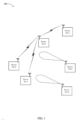
- FIG. 1 illustrates an example of an environment 100 that supports a signal converter with a variable sampling range in accordance with examples as disclosed herein.
- One or more devices may be present within the environment 100.
- the devices e.g., first device 105-1 through sixth device 105-6) may be capable of transmitting and receiving wireless signals at radio frequencies (which may also be referred to as RF signals).
- the devices may include one or more antennas to support the transmission and reception of wireless signals.
- the devices may be (or include) personal electronic devices, such as mobile devices (e.g., phones, radios, laptops, tablets, personal digital assistants, electronic readers, etc.) and other less mobile devices (e.g., desktops, televisions, servers, etc.).
- the mobile devices and/or other devices may be included in mobile vehicles (e.g., automobiles, nautical vessels, airplanes, satellites, etc.) - thus, otherwise stationary devices (e.g., the less mobile devices) may become mobile devices.
- the devices may support device-to-device (D2D) communications (e.g., using Bluetooth or other D2D protocols). Additionally, or alternatively, the devices may use one or more access networks to facilitate communications with other devices. For example, the devices may use a cellular access network, a local access network (e.g., using Wi-Fi), or a satellite access network to communicate with other devices. In some examples, one or more of the devices are a part of an access network - e.g., second device 105-2 may be a satellite in a satellite access network. In such cases, second device 105-2 may relay signals between first device 105-1 and third device 105-3 - in some examples, third device 105-3 may be (or be a part of) a ground station in a satellite access network.
- D2D device-to-device
- second device 105-2 may be a cell tower and may relay signals between first device 105-1 and third device 105-3 - in some examples, third device 105-3 may be a user device or a server of a data network, among other options.
- Fourth device 105-4 may also communicate with second device 105-2 - e.g., in some examples, fourth device 105-4 may have a subscription to a same access network as first device 105-1.
- a device may include circuitry for generating and transmitting wireless signals to other devices.
- the device may also include circuitry for receiving, and processing wireless signals emitted by other sources.
- the circuitry for transmitting wireless signals may be referred to as a transmit chain, and the circuitry for receiving wireless signals may be referred to as a receive chain.
- wireless signals transmitted by some devices may interfere with the communication of wireless signals to other devices. Communications by devices within a frequency band of the receiver may interfere with one another - e.g., transmissions by the fourth device 105-4 may interfere with communications for the first device 105-1 where the first device 105-1 and the fourth device 105-4 have similar or the same frequency bands. Similarly, communications by devices that use other bands or that are performing D2D communications may interfere with other devices - e.g., transmissions by fifth device 105-5 may interfere with communications for the first device 105-1 where the fifth device 105-5 and the first device 105-1 have similar or the same frequency bands.
- the signal converter may be configured to support direct sampling techniques.
- the receiver of the device may employ successive interference cancellation (SIC) and may thus extract different signals having different amounts of power both above and below the noise floor.
- SIC successive interference cancellation
- the signal converter may be configured to capture samples of the wireless signals using a periodic sampling interval.
- the signal converter may be configured with a sampling range (which may also be referred to as a dynamic range) that is large enough to capture the extremes of the wireless signals.
- a "clipping" condition may occur at the signal converter - e.g., the output of the signal converter may be referred to as "clipped.”
- the signal converter may be configured to have a large sampling range - e.g., a sampling range that is large enough to encompass a high-power wireless signal level. That said, if the sampling range of the signal converter is increased without also increasing a sampling resolution of the signal converter, the signal converter may again lose the capability of detecting the information signal embedded in the received wireless signal (e.g., a low-power information signal that is hidden at or below the minimum sampling resolution, a low-power information signal that is drowned out by a higher-power interfering signal, and so forth). In some examples, the capability of detecting the information signal is lost because variations in the information signal level may happen with two levels that are separated by a unit of the sampling resolution. Thus, the signal converter may be unable to detect such variations in the information signal corresponding to different data values of the information signal.
- a large sampling range e.g., a sampling range that is large enough to encompass a high-power wireless signal level. That said, if the sampling range of the signal converter is increased without also increasing
- the receiver may be configured with the signal converter that is capable of changing its sampling range while maintaining its sampling resolution step size at or below a sampling resolution step size threshold (e.g., a sampling resolution step size threshold associated with sampling signal values of an information signal when received as part of a high-power wireless signal or a lower power wireless signals). Maintaining the sampling resolution step size at or below the sampling resolution threshold may include increasing the sampling resolution of the receiver (e.g., decreasing the sampling resolution step size).
- the sampling range of the signal converter may be adaptable by enabling and disabling one or more elements (e.g., comparators) in the signal converter such that the sampling resolution is maintained.
- the sampling range of the signal converter may be adaptable, and the sampling resolution of the signal converter may be maintained by increasing or decreasing a quantity of approximation cycles applied to each analog sample. Based on adapting the sampling range of the signal converter while maintaining the sampling resolution step size at or below the sampling resolution step size threshold, a bit-width of samples output by the signal converter may change.
- a device may sample, during a first time period, a first analog signal output by an antenna array of the device.
- the device may sample the first analog signal in accordance with a first sampling range and a sampling resolution over the first sampling range.
- the device may output, during the first time period, a first digital sequence based on sampling the first analog signal.
- the device may adapt the first sampling range to a second sampling range while maintaining the sampling resolution step size at or below the sampling resolution step size threshold - e.g., after sampling the first analog signal or while sampling the first analog signal.
- maintaining the sampling resolution step size at or below the sampling resolution step size threshold may include increasing the sampling resolution of the receiver (e.g., using a finer sampling resolution step size).
- the device may adapt the sampling range based on an interference metric, where the interference metric may be based on a magnitude of the first analog signal, a magnitude of an interference signal detected by the device, an expected level of interference in a geographic area entered by the device, a time-of-day, a scheduled transmission from the device, a scheduled or anticipated transmission of neighboring devices, etc.
- a width of the second sampling range (e.g., a difference between a highest and lowest value of the second sampling range) may be larger than a width of the first sampling range.
- the device may sample a second analog signal in accordance with the second sampling range and the sampling resolution over the second sampling range.
- the second analog signal is the same as the first analog signal.
- a first portion of an analog signal may include the first analog signal and a second portion of the analog signal may include the second analog signal.
- the first analog signal and the second analog signal may be separate signals- e.g., signals that are separated in time and not merely different portions of the same analog signal. Based on the sampling during the second time period, the device may output a second digital sequence.
- the power consumption of the receiver may be adapted to be sufficient for processing the wireless signals without losing an underlying information signal. That is, the power consumption of the receiver may be reduced when lower-power wireless signals are received and increased when higher-power wireless signals are received.
- the bit-width of the digital samples output by the signal converter may be adapted to be sufficient for conveying all of the levels detectable by the signal converter.
- a throughput of digital samples through a system using the receiver may be increased when smaller bit-widths are used - e.g., because the bandwidth of an interface may support the communication of more digital samples in an interval.
- generating digital samples having smaller bit-widths may result in reduced processing complexity and/or power consumption throughout the system.
- a beamformer and processor may process the digital samples using less power and with simpler arithmetic components than if larger bit-widths are used.
- the beamformer may use the reduced complexity to increase a quantity of beams signals that can be generated by the beamformer.
- the quantity of beam signals output by the beamformer may be increased when smaller bit-width digital samples are used - e.g., because a processing complexity of the digital samples may decrease or because the overall throughput of the beam data has been decreased.
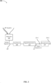
- FIG. 2 illustrates an example of a receiver that supports a signal converter with a variable sampling range in accordance with examples as disclosed herein.
- Receiver 200 may be configured to detect wireless signals (e.g., RF signals), convert the detected wireless signals to digital signals, and process the digital signals to obtain beam signals, or any combination thereof.
- Receiver 200 may include one or more antennas 205, one or more amplifiers 210, one or more signal converters 215, interfaces 219, and beamformer 220.
- An amplifier of the one or more amplifiers 210 may be configured to amplify low-power signals (e.g., a signal detected by a respective antenna) with little to no effect on the signal-to-noise ratio of the low-power signal.
- One or more amplifiers 210 may include one or more low noise amplifiers.
- respective low-noise amplifiers are coupled with respective antennas of the one or more antennas 205.
- respective signal converters of the one or more signal converters 215 may be configured to sample a respective analog signal of the one or more analog signals 207 (e.g., in accordance with a periodic sampling interval). For each sample of the respective analog signal taken by the respective signal converter, the respective signal converter may be configured to output a digital representation of the corresponding sample (which may be referred to as a digital sample).
- the digital sample may be represented using one or more bits. In some examples, the quantity of bits used to represent the digital sample is based on a quantity of levels that can be detected by the signal converter.
- the respective signal converter may output, via first interface 219-1, a digital sample stream including the digital samples taken of the respective analog signal.
- the respective signal converter may receive multiple analog signals of the one or more analog signals 207 and may output multiple digital sequences of the one or more digital sequences 217, where each digital sequence may include a digital sample stream for each analog signal of the one or more analog signals 207 received at the signal converter.
- the signal converter 215 may be configured with the sampling range that is large enough to support the voltage range of the high-power signals while maintaining the sampling resolution step size to detect the low-power signals. Accordingly, a quantity of bits used to represent a digital sample obtained by a signal converter that is configured to process both high and low-power signals may be increased relative to a signal converter that is configured to process signals within a smaller range. As also described herein, as a quantity of bits output by a signal converter increases, the power consumption of the signal converter may also increase.
- a sampling range of the signal converter may be adaptable based on a magnitude of signals currently being input to the signal converter while the sampling resolution step size of the signal converter may be maintained at a same resolution or below a sampling resolution step size. For example, while receiving low-power signals, the sampling range of the signal converter may be adapted to a first range and while receiving high-power signals, the sampling range of the signal converter may be adapted to a second range that is larger than the first range. Accordingly, a quantity of bits used to represent digital samples output by the signal converter may similarly be adaptable based on the magnitude of signals currently being input to the signal converter.
- First interface 219-1 may be configured to convey data from the one or more signal converters 215 to other components in a device that includes receiver 200.
- first interface 219-1 may be configured to communicate data up to an upper data rate (which may be referred to as an achievable data rate).
- the achievable data rate of first interface 219-1 may be measured in bits or bytes per second (e.g., 10 GB/s).
- the achievable sample rate of first interface 219-1 (the rate at which digital samples may be communicated over first interface 219-1) may be based on the achievable data rate and a bit-width of the digital samples - e.g., the achievable sample rate may be determined by dividing the achievable data rate by the bit-width of the digital samples).
- Beamformer 220 may be configured to generate beam signals based on a set of digital sample streams received from the one or more signal converters 215. To generate the beam signals, beamformer 220 may apply beam weights to time-aligned digital samples received in the set of digital samples to obtain beam signals, where each beam weight may include a set of beam coefficients for each beam signal generated by beamformer 220. Based on applying the beam weights, beamformer 220 may obtain multiple weighted versions of the time-aligned digital samples. To generate the beam signals, beamformer 220 may further add, for each beam signal, a respective weighted version of the time-aligned digital samples to obtain a beam sample for a beam signal, where a beam signal may include successive beam samples.
- adapting the bit-width of digital samples output by the one or more signal converters 215 may result in the increased throughput of data in receiver 200.
- adapting the bit-width of the digital samples may decrease a processing burden on beamformer 220 when the signal converter receives low-power signals that are detectable with a smaller sampling range - e.g., by simplifying the arithmetic operations performed by beamformer 220.
- the reduction in processing complexity at beamformer 220 may enable the beamformer 220 to generate an increased quantity of beam signals when the signal converter receives low-power signals that are able to be processed with a smaller sampling range.
- beamformer 220 may be configured with a variable-bit adder that can be used to add two digital samples having a first bit-width at a time or to simultaneously add two sets of two digital samples having a smaller second bit-width at a time.
- beamformer 220 determines whether to adapt the quantity of beam signals based on the wireless signal detected by the one or more antennas (e.g., interference metrics associated with the wireless signal, a magnitude of the wireless signal, etc.), based on a control signal (e.g., received from the one or more signal converters 215), or both. Options for implementing and adapting the output of beamformer 220 are described in more detail herein.
- Second interface 219-2 may be configured to convey data from beamformer 220 to other components (e.g., a processor) in a device that includes receiver 200.
- second interface 219-2 may be configured to communicate data up to an achievable data rate, which may be equivalent to or greater than the achievable data rate of first interface 219-1.
- beamformer 220 may determine a quantity of beam signals to output based on an achievable data rate of second interface 219-2, a bit-width of digital samples received from the one or more signal converters 215, and a rate at which digital samples are received from the one or more signal converters 215 (which may correspond to a sampling frequency of the one or more signal converters 215).
- FIG. 3A illustrates an example of a signal converter 315-a with variable sampling range in accordance with examples as disclosed herein.
- Signal converter 315-a may be configured to output a stream of digital samples (which may be referred to as a digital sample stream), where the digital samples may have different bit-widths based on toggling an activation of one or more of the component ADCs 305-a.
- Signal converter 315-a may be configured to adapt the bit-widths of the digital samples based on input signal 303-a received at signal converter 315-a - e.g., a magnitude of input signal 303-a, interference metrics associated with the input signal 303-a, etc.
- Input signal 303-a may be equivalent to an analog signal output by an antenna (e.g., an analog signal of the one or more analog signals 207 of FIG. 2 ) or an amplified version of an analog signal output by an amplifier coupled with the antenna.
- Signal converter 315-a may be an example of the one or more signal converters 215 of FIG. 2 .
- Signal converter 315-a may include first component ADC 305-a1, second component ADC 305-a2, third component ADC 305-a3, and decoder 320-a. Signal converter 315-a may toggle an activation of second component ADC 305-a2, third component ADC 305-a3, or both, based on a desired sampling range and bit-width for digital samples output by signal converter 315-a. In some examples, a signal for enabling/disabling third component ADC 305-a3 may be received via third enable line 310-a3, and a signal for enabling/disabling second component ADC 305-a2 may be received via second enable line 310-a2.
- signal converter 315-a may disable second component ADC 305-a2 and third component ADC 305-a3, while the first component ADC 305-a1 may be enabled.
- signal converter 315-a may disable third component ADC 305-a3, while first component ADC 305-a1 and second component ADC 305-a2 may be enabled.
- signal converter 315-a may enable each of the component ADCs 305-a.
- the third sampling range and third bit-width may be larger than the second sampling range and second bit-width, and the second sampling range and the second bit-width may be larger than the first sampling range and the first bit-width.
- the sampling resolution of signal converter 315-a may be maintained independent of changes to the sampling range of signal converter 315-a. In some examples, the sampling resolution of signal converter 315-a may change when the sampling range of signal converter 315-a is adapted, but the sampling resolution step size may remain at or below a sampling resolution step size threshold.
- Decoder 320-a may be configured to convert the code output by the component ADCs 305-a to a multi-bit digital sample that includes a binary representation of the analog level of input signal 303-a.
- the bit-width of the digital sample output by decoder 320-a is based on whether second component ADC 305-a2 and third component ADC 305-a3 are enabled or disabled. For example, if second component ADC 305-a2 and third component ADC 305-a3 are disabled, decoder 320-a may output digital samples having a first bit-width based on an output of first component ADC 305-a1 (which may correspond to bits zero to three of four-bit digital samples output by the so configured decoder 320-a).
- a DC offset may be applied to input signal 303-a based on which of the component ADCs 305-a are enabled/disabled. For example, the DC offset may be applied to center input signal 303-a between a lower limit and upper limit of the configured sampling range of signal converter 315-a. For example, if third component ADC 305-a3 is disabled, the DC offset may be configured to center input signal 303-a between a lower limit of the second sampling range and an upper limit of the second sampling range that is configured for signal converter 315-a by using first component ADC 305-a1 and second component ADC 305-a2.
- the DC offset may be configured to center input signal 303-a between a lower limit of the first sampling range and an upper limit of the first sampling range that is configured for the signal converter 315-a by using the first component ADC 305-a1, and so forth.
- FIG. 3B illustrates an example of a signal converter 315-b with variable sampling range in accordance with examples as disclosed herein.
- Signal converter 315-b may toggle an activation of first component ADC 305-b1 and third component ADC 305-b3 based on a desired sampling range and bit-width for digital samples. For example, to achieve a first sampling range and output digital samples with a first bit-width, signal converter 315-b may disable first component ADC 305-b1 and third component ADC 305-b3. To achieve a second sampling range and output digital samples with a second bit-width, signal converter 315-b may enable first component ADC 305-b1 and third component ADC 305-b3. The second sampling range and second bit-width may be larger than the first sampling range and first bit-width. In some examples, a signal for enabling/disabling first component ADC 305-b1 and third component ADC 305-b3 may be received via enable line 310-b.
- an operation for adding a DC offset to an input signal 303-b may be omitted. That is, the sampling range of signal converter 315-b may remain centered around a common level regardless of whether only second component ADC 305-b2 is enabled or all of the component ADCs 305-b are enabled. Thus, the DC offset may not be applied to input signal 303-b to center input signal 303-b between the lower limit and upper limit of the sampling range as different combinations of the component ADCs 305-b are enabled/disabled.
- the first set of the comparators 410-a corresponds to the upper portion of the comparators 410-a and a first set of bits (e.g., [12:15]) of a digital sample output by decoder 420-a
- the second set of the comparators 410-a corresponds to the middle portion of the comparators 410-a and a second set of bits (e.g., [4:11]) of the digital sample
- the third set of the comparators 410-a corresponds to a lower portion of the comparators 410-a and a third set of bits (e.g., [0:3]) of the digital sample.
- successive approximation register 445-b may determine whether to keep the third most significant bit of the code as a 1 or change it to a 0.
- the above process may continue for up to N approximation cycles within the sampling period.
- another bit of the code may be determined and, thus, a digital representation of the voltage level output by sample-and-hold circuit 435-b may be determined with increased precision and with a higher resolution than exists with the prior approximation cycle.
- a quantity of approximation cycles performed within a sampling period may be increased (e.g., proportionally).
- the power consumed by signal converter 415-b per digital sample may increase (e.g., proportionally) with the number of approximation cycles performed during a sampling period.
- the sampling range of the signal converter 415-b may be set to a first sampling range and a first quantity of approximation cycles may be configured within the sampling period - e.g., to achieve a sampling resolution for the first sampling range.
- the sampling range of the signal converter 415-b may be set to a second sampling range and a second quantity of approximation cycles may be configured within the sampling period. In some examples, the second quantity of approximation cycles is selected to maintain the sampling resolution. In some examples, if the magnitude of input signal 403-b is at or above a second threshold, the sampling range of the signal converter 415-b may be set to a third sampling range and a third quantity of approximation cycles may be configured within the sampling period. In some examples, the third quantity of approximation cycles is selected to maintain the sampling resolution.
- the third sampling range and the third quantity of approximation cycles may be greater than the second sampling range and the second quantity of approximation cycles, and the second sampling range and the second quantity of approximation cycles may be greater than the first sampling range and the first quantity of approximation cycles.
- the sampling resolution is maintained independent of adapting the sampling range of signal converter 415-b.
- the sampling resolution step size is maintained below a sampling resolution step size threshold independent of adapting the sampling range of signal converter 415-b.
- FIG. 5 illustrates an example of a beamformer 520 that supports a signal converter with variable sampling range in accordance with examples as disclosed herein.
- Beamformer 520 may be configured to process digital versions of an analog signal detected by an array of antennas (e.g., after processing by amplifiers, signal converters, etc.). Beamformer 520 may be further configured to apply beam weight sets to the digital versions to generate multiple beam signals that correspond to different signals embedded within the analog signal, where the different signals may be received at the array of antennas from different directions. Each beam weight set may correspond to a respective beam signal and include a set of beam coefficients. Beamformer 520 may include a weighting component 505 and variable-bit adders 510. Beamformer 520 may be an example of beamformer 220 of FIG. 2 .
- Weighting component 505 may be configured to apply the beam weight sets to digital samples of a digital sample stream received at weighting component 505 (e.g., from a signal converter, such as the one or more signal converters 215 of FIG. 2 ). During a first interval, weighting component 505 may receive a set of digital samples, x (which may include digital samples [ x 0 , x 1 , x 2 , x 3 ]) , corresponding to the digital versions of the analog signal received at each antenna of the antenna array.
- x which may include digital samples [ x 0 , x 1 , x 2 , x 3 ]
- Weighting component 505 may apply each beam weight set to the received set of digital samples. For example, weighting component 505 may apply the first beam weight set w A (which may include beam coefficients [ w A 0 , w A 1 , w A 2 , w A 3 ]) to the set of digital samples [ x 0 , x 1 , x 2 , x 3 ] , and the second beam weight set w B to the set of digital samples. In some examples, weighting component 505 may also apply the third beam weight set w C to the set of digital samples and the fourth beam weight set w D to the set of digital samples - e.g., based on a bit-width of the digital samples.
- first beam weight set w A which may include beam coefficients [ w A 0 , w A 1 , w A 2 , w A 3 ]
- weighting component 505 may also apply the third beam weight set w C to the set of digital samples and the fourth beam weight set w D
- weighting component 505 include one or more multipliers that are used to multiply a digital sample by a corresponding beam coefficient. After applying the beam weight sets to the set of digital samples, weighting component 505 may output the weighted sets of digital samples to one or more adders.
- first variable-bit adder 510-1 may be configured to add the first set of weighted digital samples ( w A ⁇ x ) to obtain digital samples of a first beam signal y 0 .
- second variable-bit adder 510-2 may be configured to add the second set of weighted digital samples ( w B ⁇ x ) to obtain digital samples of a second beam signal y 1 .
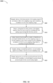
- One or more of the operations described in flowchart 600 may be performed earlier or later, omitted, replaced, supplemented, or combined with another operation. Also, additional operations described herein may replace, supplement or be combined with one or more of the operations described in flowchart 600.
- parameters of a beamformer may be configured.
- the beamformer is configured to output a first quantity of beam signals based on the bit-width of digital samples output by the signal converter.
- the beamformer is configured to output the first quantity of beam signals when the digital samples have a first bit-width and a second quantity of beam signals when the digital samples have a second bit-width.
- the first quantity of beam signals is larger than the second quantity of beam signals, and the first bit-width is smaller than the second bit-width.
- a set of analog signals may be generated based on a detected wireless signal.
- each antenna of an antenna array e.g., the one or more antennas 205 of FIG. 2
- the analog signals output by the antennas of the antenna array may be amplified (e.g., by the one or more amplifiers 210 of FIG. 2 ).
- the amplification is a low-noise amplification.
- Each amplifier of the amplifiers may be coupled with one or more respective antennas of the antenna array.
- metrics for the analog signals may be determined. For example, a magnitude of the analog signals is determined, an amount of interference associated with the analog signals may be determined, an expected amount of interference associated with the analog signals may be determined, or any combination thereof.
- the determination of whether to reconfigure the parameters of the signal converter may include determining whether a magnitude of the analog signal is exceeding a threshold range. In some examples, it is determined that the magnitude of the analog signal is exceeding the threshold range based on the extremes of the analog signal exceeding the lower limit and/or upper limit of the threshold limit.
- the analog signal 710-b of FIG. 7B depicts an example of an analog signal that increases in magnitude such that the upper and lower limits of the analog signal exceed the upper and lower limits of the threshold range 715-b configured for the signal converter.
- a determination to reconfigure the parameters of the signal converter may be made.
- a determination to reconfigure the parameters of the signal converter may be made.
- a sampling range of a signal converter may be increased based on determining that an expected amount of interference for the analog signal exceeds a threshold. Conversely, the sampling range of the signal converter may be decreased based on determining that the expected amount of interference is at or below the threshold.
- components of the signal converter may also be adapted - e.g., to maintain a sampling resolution step size of the signal converter at a same level, below a sampling resolution step size threshold, or both. For example, if the sampling range of the signal converter is increased, a quantity of comparators used to process the analog signal may be increased, as described with reference to FIG. 4A . Additionally, a decoder may be configured to process the signals output by the newly enabled comparators and to output digital samples with an increased bit-width. Alternatively, if the sampling range of the signal converter is decreased, a quantity of comparators used to process the analog signal may be decreased, as described with reference to FIG. 4A . Additionally, the decoder may be configured to ignore the signals output by the newly disabled comparators and to output digital samples with a decreased bit-width.
- a quantity of approximation cycles used to process the analog signal may be increased, as described with reference to FIG. 4B .
- a quantity of approximation cycles used to process the analog signal may be decreased, as also described with reference to FIG. 4B .
- a bit-width of digital samples output by the signal converter may change as the parameters (e.g., the sampling range and sampling resolution step size) of the signal converter are adapted.
- the bit-width of the digital samples may increase when the sampling range is increased and decrease when the sampling range is decreased.
- an indication that the signal converter has been reconfigured (and thus that the bit-width of digital samples has been adapted) may be provided to additional components within the device, including a beamformer, a processor, or both.
- a sampling frequency of the signal converter (and a throughput of data through a device) may be increased.
- a sampling frequency of the signal converter (and a throughput of data through a device) may be decreased.
- parameters of the beamformer may be reconfigured - e.g., based on the parameters of the signal converter being reconfigured.
- the beamformer may be reconfigured to support generating a second quantity of beam signals based on the bit-widths of digital samples output by the reconfigured signal converter.
- arithmetic components e.g., adders and/or multipliers
- within the beamformer may be reconfigured to support digital samples of larger or smaller bit-widths.
- the beamformer may be reconfigured to generate a smaller quantity of beam signals (e.g., two beam signals). For example, the beamformer may apply two beam weights to incoming digital signals (e.g., instead of four) and may output the first weighted signal to a first adder (which may be fully utilized by the bit-width of the digital signals) and the second weighted signal to a second adder (which may also be fully utilized by the bit-width of the digital signals).
- the first adder may be an example of first variable-bit adder 510-1 of FIG. 5 and the second adder may be an example of second variable-bit adder 510-2 of FIG. 5 .
- the beamformer may be reconfigured to generate a same or greater quantity of beam signals (e.g., four beam signals).
- a quantity of beams output by the beamformer may be maintained if the sampling frequency of a signal converter is increased based on reconfiguring the signal converter - e.g., if increasing the sampling frequency and quantity of beams would exceed a capacity of an interface.
- the analog signals may be converted to digital signals - e.g., by the signal converter.
- the digital signal may include a stream of digital samples, where a bit-width of the digital samples may be based on a configured sampling range and sampling resolution step size of the signal converter.
- the digital signals correspond to analog signals generated by one or more antennas of an antenna array.
- beam signals may be generated from the digital signals - e.g., by the beamformer.
- the beamformer may apply beam weights to the digital signals, where the quantity of beam weights applied to the digital signals may be based on a bit-width of the digital samples in the digital signals.
- Generating the beam signals may include multiplying the digital samples by respective beam coefficients of respective beam weights and adding the respective weighted digital samples together.
- FIG. 7A illustrates a signal diagram 700-a for a signal converter with variable sampling range in accordance with examples as disclosed herein.
- Signal diagram 700-a may depict analog signal 710-a with reference to a sampling range 705-a of a signal converter.
- signal diagram 700-a may further depict the extremes of analog signal 710-a exceeding the sampling range 705-a of the signal converter, resulting in a clipping condition at the signal converter - e.g., as the extremes of the analog signal may be outside of a detectable range of the signal converter.
- signal diagram 700-a may depict the increase of the sampling range 705-a of the signal converter in response to the detection of the clipping condition.
- the analog signal 710-a and sampling range 705-a of the signal converter depicted in FIG. 7A may be normalized around a zeroed axis - e.g., despite having a DC offset.
- FIG. 7B illustrates a signal diagram 700-b for a signal converter with variable sampling range in accordance with examples as disclosed herein.
- Signal diagram 700-b may depict analog signal 710-b with reference to a sampling range 705-b of a signal converter and a threshold range 715-b.
- signal diagram 700-b may further depict the extremes of analog signal 710-b exceeding the threshold range 715-b configured for the signal converter.
- signal diagram 700-b may depict the increase of the sampling range 705-b of the signal converter in response to the detection of the threshold range 715-b being exceeded as well as the increase of the threshold range 715-b.
- the analog signal 710-a and sampling range 705-a of the signal converter depicted in FIG. 7A may be normalized around a zeroed axis- e.g., despite having a DC offset.
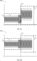
- FIG. 8A illustrates a signal diagram 800-a for a signal converter with variable sampling range in accordance with examples as disclosed herein.
- Signal diagram 800-a may depict analog signal 810-a without normalization about a zeroed axis.
- analog signal 810-a may no longer be centered between the lower limit and upper limit of the sampling range 805-a of the signal converter - e.g., based on a threshold voltage for determining a least significant bit having a fixed voltage.
- signal diagram 800-a may depict an operation of a signal converter configured in accordance with FIG. 3A or 4A .
- a DC offset may be added to analog signal 810-a such that analog signal 810-a is centered between the lower limit and upper limit of the sampling range 805-a of the signal converter after the sampling range 805-a of the signal converter is adapted at time t1 825-a.
- the DC offset may similarly be applied to threshold limit 815-a such that analog signal 810-a is centered between the upper and lower limits of threshold limit 815-a.
- Threshold limit 815-a may include one or more threshold limits, with a first threshold limit shown prior to time t1 825-a and a second threshold limit shown subsequent to time t1 825-a.
- the sampling range 805-a of the signal converter may be decreased if the analog signal 810-a is no longer above the first threshold limit (e.g., for a certain period of time).
- the sampling range 805-a of the signal converter may be increased if the analog signal 810-a is above the second threshold limit (e.g., for a certain period of time).
- Threshold limit 815-b may include one or more threshold limits, with a first threshold limit shown prior to time t1 825-b and a second threshold limit shown subsequent to time t1 825-b.
- the sampling range 805-b of the signal converter may be decreased if the analog signal 810-b is no longer above the first threshold limit (e.g., for a certain period of time).
- the sampling range 805-b of the signal converter may be increased if the analog signal 810-b is above the second threshold limit (e.g., for a certain period of time).
- signal diagram 800-b may depict an operation of a signal converter configured in accordance with FIG. 3B .
- FIG. 9 shows an example controller 900 that supports a signal converter with variable sampling range in accordance with examples described herein.
- Controller 900 may be an example of aspects of a communications device as described with reference to FIGs. 1 through 8 . Controller 900, or various components thereof, may be an example of means for performing various aspects of the signal converter with variable dynamic range as described herein.
- controller 900 may include sampling component 925, output component 930, adaptation component 935, interference component 940, arithmetic component 945, beamforming component 950, or any combination thereof. Each of these components may communicate, directly or indirectly, with one another (e.g., via one or more buses).
- the controller 900 may be implemented in hardware (e.g., in communications management circuitry).
- the hardware may include a processor, a DSP, an ASIC, an FPGA or other programmable logic device, a discrete gate or transistor logic, discrete hardware components, or any combination thereof configured as or otherwise supporting a means for performing the functions described in the present disclosure.
- a processor and memory coupled with the processor may be configured to perform one or more of the functions described herein (e.g., by executing, by the processor, instructions stored in the memory).
- controller 900 transmits signaling that reconfigures a mode of a component of receiver 200.
- controller 900 may configure the one or more signal converters 215 to use a higher dynamic range based on determining that an interference metric exceeds a threshold. Based on configuring the higher dynamic range at the one or more signal converters 215, the controller may indicate to beamformer 220 of FIG. 2 to reduce a quantity of beam signals generated at beamformer 220.
- controller 900 may configure the one or more signal converters 215 to use a lower dynamic range based on determining that an interference metric is below a threshold and configure beamformer 220 to increase a quantity of generated beam signals.
- Adaptation component 935 may be configured as or otherwise support a means for adapting, based at least in part on a metric of interference associated with the device, the first sampling range to a second sampling range while maintaining the sampling resolution step size over the second sampling range.
- sampling component 925 may be configured as or otherwise support a means for sampling, during a second time period, a second analog signal in accordance with the second sampling range.
- output component 930 may be configured as or otherwise support a means for outputting, during the second time period and based at least in part on the sampling, a second digital sequence based at least in part on the second analog signal.
- generating the plurality of first beam signals includes inputting a first portion of the first plurality of samples to a first portion of an adder of a beamformer and a second portion of the first plurality of samples to a second portion of the adder of the beamformer, the first portion of the adder being associated with a first communication signal and the second portion of the adder being associated with a second communication signal, and generating the plurality of second beam signals includes inputting the second plurality of samples to the first portion of the adder and the second portion of the adder, the adder being associated with the first communication signal.
- the first analog signal and the second analog signal are sampled by the signal converter that includes a first element for sampling signals within a first voltage range and a second element for sampling signals within a second voltage range that is greater than the first voltage range
- interference component 940 may be configured as or otherwise support a means for determining that interference in an area is below an interference threshold.
- the first analog signal and the second analog signal are sampled by the signal converter that includes a first element for sampling signals within a first voltage range and a second element for sampling signals within a second voltage range that is greater than the first voltage range
- adaptation component 935 may be configured as or otherwise support a means for adapting the second sampling range to the first sampling range based at least in part on the interference being below the interference threshold, where adapting the second sampling range to the first sampling range includes disabling the second element.
- the first analog signal and the second analog signal are sampled by the signal converter that includes a first element for sampling signals within a first voltage range and a second element for sampling signals within a second voltage range that is greater than the first voltage range
- interference component 940 may be configured as or otherwise support a means for determining that interference is above an interference threshold in an area, where adapting the first sampling range to the second sampling range includes enabling the second element based at least in part on the interference being above the interference threshold.
- the first element includes a first set of comparators and the second element includes a second set of comparators.
- the first analog signal and the second analog signal are sampled by the signal converter that includes a successive approximation circuit
- interference component 940 may be configured as or otherwise support a means for determining that interference in an area is above an interference threshold, where adapting the first sampling range to the second sampling range includes increasing a quantity of approximation cycles applied by the successive approximation circuit to an analog sample based at least in part on the interference being above the interference threshold.
- the set of operations may include sampling, during a first time period, a first analog signal in accordance with a first sampling range and a sampling resolution step size over the first sampling range.
- the operations of 1005 may be performed in accordance with examples as disclosed herein. In some examples, aspects of the operations of 1005 may be performed by a sampling component 925 as described with reference to FIG. 9 .
- the functions described herein may be implemented in hardware, software executed by a processor, firmware, or any combination thereof. If implemented in software executed by a processor, the functions may be stored on or transmitted over as one or more instructions or code on a computer-readable medium. Other examples and implementations are within the scope of the disclosure and appended claims. For example, due to the nature of software, functions described herein can be implemented using software executed by a processor, hardware, firmware, hardwiring, or combinations of any of these. Features implementing functions may also be physically located at various positions, including being distributed such that portions of functions are implemented at different physical locations.
- Computer-readable media includes both non-transitory computer storage media and communication media including any medium that facilitates transfer of a computer program from one place to another.
- a non-transitory storage medium may be any available medium that can be accessed by a general purpose or special purpose computer.
- non-transitory computer-readable media may include RAM, ROM, electrically erasable programmable read-only memory (EEPROM), flash memory, compact disk read-only memory (CDROM) or other optical disk storage, magnetic disk storage or other magnetic storage devices, or any other non-transitory medium that can be used to carry or store desired program code means in the form of instructions or data structures and that can be accessed by a general-purpose or special-purpose computer, or a general-purpose or special-purpose processor.
- any connection is properly termed a computer-readable medium.
- the software is transmitted from a website, server, or other remote source using a coaxial cable, fiber optic cable, twisted pair, digital subscriber line (DSL), or wireless technologies such as infrared, radio, and microwave
- the coaxial cable, fiber optic cable, twisted pair, DSL, or wireless technologies such as infrared, radio, and microwave are included in the definition of medium.
- Disk and disc include CD, laser disc, optical disc, digital versatile disc (DVD), floppy disk and Blu-ray disc where disks usually reproduce data magnetically, while discs reproduce data optically with lasers. Combinations of the above are also included within the scope of computer-readable media.
Landscapes
- Engineering & Computer Science (AREA)
- Computer Networks & Wireless Communication (AREA)
- Signal Processing (AREA)
- Theoretical Computer Science (AREA)
- Quality & Reliability (AREA)
- Physics & Mathematics (AREA)
- Electromagnetism (AREA)
- Analogue/Digital Conversion (AREA)
- Noise Elimination (AREA)
- Time-Division Multiplex Systems (AREA)
Applications Claiming Priority (3)
| Application Number | Priority Date | Filing Date | Title |
|---|---|---|---|
| US202163168236P | 2021-03-30 | 2021-03-30 | |
| PCT/US2022/022406 WO2022212418A1 (en) | 2021-03-30 | 2022-03-29 | System and method for sampling signals |
| EP22723235.2A EP4302405B1 (de) | 2021-03-30 | 2022-03-29 | System und verfahren zur abtastung von signalen |
Related Parent Applications (1)
| Application Number | Title | Priority Date | Filing Date |
|---|---|---|---|
| EP22723235.2A Division EP4302405B1 (de) | 2021-03-30 | 2022-03-29 | System und verfahren zur abtastung von signalen |
Publications (2)
| Publication Number | Publication Date |
|---|---|
| EP4535667A2 true EP4535667A2 (de) | 2025-04-09 |
| EP4535667A3 EP4535667A3 (de) | 2025-05-21 |
Family
ID=81648836
Family Applications (2)
| Application Number | Title | Priority Date | Filing Date |
|---|---|---|---|
| EP25157245.9A Pending EP4535667A3 (de) | 2021-03-30 | 2022-03-29 | System und verfahren zur abtastung von signalen |
| EP22723235.2A Active EP4302405B1 (de) | 2021-03-30 | 2022-03-29 | System und verfahren zur abtastung von signalen |
Family Applications After (1)
| Application Number | Title | Priority Date | Filing Date |
|---|---|---|---|
| EP22723235.2A Active EP4302405B1 (de) | 2021-03-30 | 2022-03-29 | System und verfahren zur abtastung von signalen |
Country Status (7)
| Country | Link |
|---|---|
| US (1) | US20240178850A1 (de) |
| EP (2) | EP4535667A3 (de) |
| JP (1) | JP2024516933A (de) |
| AU (1) | AU2022249044A1 (de) |
| CA (1) | CA3213342A1 (de) |
| IL (1) | IL307296A (de) |
| WO (1) | WO2022212418A1 (de) |
Families Citing this family (4)
| Publication number | Priority date | Publication date | Assignee | Title |
|---|---|---|---|---|
| US12551155B1 (en) | 2018-12-11 | 2026-02-17 | Arrowhead Center, Inc. | Electrocardiogram sensing and processing |
| US12431913B1 (en) | 2022-06-22 | 2025-09-30 | Arrowhead Center, Inc. | Dynamic predictive sampling and processing |
| EP4668594A1 (de) * | 2024-06-21 | 2025-12-24 | Nxp B.V. | Nahfeldkommunikationsvorrichtung und betriebsverfahren |
| CN121099401B (zh) * | 2025-09-20 | 2026-04-03 | 苏州陆和电子有限公司 | 高能效模数转换无线接收器及功耗优化方法 |
Family Cites Families (5)
| Publication number | Priority date | Publication date | Assignee | Title |
|---|---|---|---|---|
| GB0423011D0 (en) * | 2004-10-16 | 2004-11-17 | Koninkl Philips Electronics Nv | Method and apparatus for analogue to digital conversion |
| WO2009034618A1 (ja) * | 2007-09-11 | 2009-03-19 | Panasonic Corporation | 無線受信機 |
| US20090154612A1 (en) * | 2007-12-12 | 2009-06-18 | Ahmadreza Rofougaran | Method and system for dynamic filtering and data conversion resolution adjustments in a receiver |
| US10230384B2 (en) * | 2016-12-09 | 2019-03-12 | Rambus Inc. | Variable resolution digital equalization |
| US10897387B1 (en) * | 2018-04-25 | 2021-01-19 | Harmonic, Inc. | Increasing ADC dynamic range by time domain selective cancellation of predictable large PAPR signals |
-
2022
- 2022-03-29 WO PCT/US2022/022406 patent/WO2022212418A1/en not_active Ceased
- 2022-03-29 AU AU2022249044A patent/AU2022249044A1/en active Pending
- 2022-03-29 EP EP25157245.9A patent/EP4535667A3/de active Pending
- 2022-03-29 EP EP22723235.2A patent/EP4302405B1/de active Active
- 2022-03-29 CA CA3213342A patent/CA3213342A1/en active Pending
- 2022-03-29 US US18/284,803 patent/US20240178850A1/en active Pending
- 2022-03-29 IL IL307296A patent/IL307296A/en unknown
- 2022-03-29 JP JP2023559704A patent/JP2024516933A/ja active Pending
Also Published As
| Publication number | Publication date |
|---|---|
| EP4302405A1 (de) | 2024-01-10 |
| EP4302405B1 (de) | 2025-02-12 |
| WO2022212418A1 (en) | 2022-10-06 |
| IL307296A (en) | 2023-11-01 |
| CA3213342A1 (en) | 2022-10-06 |
| US20240178850A1 (en) | 2024-05-30 |
| JP2024516933A (ja) | 2024-04-18 |
| AU2022249044A1 (en) | 2023-10-19 |
| EP4535667A3 (de) | 2025-05-21 |
Similar Documents
| Publication | Publication Date | Title |
|---|---|---|
| EP4535667A2 (de) | System und verfahren zur abtastung von signalen | |
| US10581442B2 (en) | Apparatus for correcting linearity of a digital-to-analog converter | |
| US10224946B2 (en) | Digital-to-analog converter (DAC) with enhanced dynamic element matching (DEM) and calibration | |
| US11223367B2 (en) | Analog-to-digital converting apparatuses and operating methods | |
| WO2021184232A1 (en) | Removal of passive intermodulation in antenna systems | |
| US9000969B2 (en) | Variable resolution data conversion in a receiver | |
| US9800254B2 (en) | Digital-to-analog converter (DAC) with partial constant switching | |
| US10516406B1 (en) | Digital to analog converter linearization system | |
| US20180091260A1 (en) | Adc bit allocation under bit constrained mu-massive mimo systems | |
| JP4934529B2 (ja) | 無線受信回路、並びに無線トランシーバ回路及びそのキャリブレーション方法 | |
| CN111491357B (zh) | 一种用于包内发射功率控制的系统和方法 | |
| US20090239496A1 (en) | Adaptive linearity communication device | |
| US10028222B2 (en) | Apparatus and method for controlling power in a communication system | |
| US9853654B2 (en) | Error-feedback digital-to-analog converter (DAC) | |
| US20150188499A1 (en) | Communication system and method for detecting loading variation of power amplifier thereof | |
| US10263636B2 (en) | Scalable dynamic range analog-to-digital converter system | |
| US20220271786A1 (en) | Radio transceiver device configured for dithering of a received signal | |
| KR20210034411A (ko) | 데이터 압축기를 포함하는 무선 통신 장치 및 이의 동작 방법 | |
| US9319062B2 (en) | Dynamic range reduction for analog-to-digital converters | |
| US11265198B1 (en) | Increasing ADC dynamic range by time domain selective cancellation of predictable large PAPR signals | |
| US9473186B2 (en) | Method of controlling receiver gain automatically and apparatus for automatic gain control in receiver | |
| WO2026012586A1 (en) | Reconfigurable pipelined sdac-ldac sar adc stage | |
| CN108289321A (zh) | 通信装置及信号处理方法 |
Legal Events
| Date | Code | Title | Description |
|---|---|---|---|
| PUAI | Public reference made under article 153(3) epc to a published international application that has entered the european phase |
Free format text: ORIGINAL CODE: 0009012 |
|
| STAA | Information on the status of an ep patent application or granted ep patent |
Free format text: STATUS: THE APPLICATION HAS BEEN PUBLISHED |
|
| AC | Divisional application: reference to earlier application |
Ref document number: 4302405 Country of ref document: EP Kind code of ref document: P |
|
| AK | Designated contracting states |
Kind code of ref document: A2 Designated state(s): AL AT BE BG CH CY CZ DE DK EE ES FI FR GB GR HR HU IE IS IT LI LT LU LV MC MK MT NL NO PL PT RO RS SE SI SK SM TR |
|
| REG | Reference to a national code |
Ref country code: DE Ref legal event code: R079 Free format text: PREVIOUS MAIN CLASS: H03M0001000000 Ipc: H04B0001000000 |
|
| PUAL | Search report despatched |
Free format text: ORIGINAL CODE: 0009013 |
|
| AK | Designated contracting states |
Kind code of ref document: A3 Designated state(s): AL AT BE BG CH CY CZ DE DK EE ES FI FR GB GR HR HU IE IS IT LI LT LU LV MC MK MT NL NO PL PT RO RS SE SI SK SM TR |
|
| RIC1 | Information provided on ipc code assigned before grant |
Ipc: H03M 1/00 20060101ALI20250411BHEP Ipc: H04B 1/16 20060101ALI20250411BHEP Ipc: H04B 1/00 20060101AFI20250411BHEP |
|
| STAA | Information on the status of an ep patent application or granted ep patent |
Free format text: STATUS: REQUEST FOR EXAMINATION WAS MADE |
|
| 17P | Request for examination filed |
Effective date: 20251120 |