EP4535689A1 - Dispositif de mesure - Google Patents
Dispositif de mesure Download PDFInfo
- Publication number
- EP4535689A1 EP4535689A1 EP23815554.3A EP23815554A EP4535689A1 EP 4535689 A1 EP4535689 A1 EP 4535689A1 EP 23815554 A EP23815554 A EP 23815554A EP 4535689 A1 EP4535689 A1 EP 4535689A1
- Authority
- EP
- European Patent Office
- Prior art keywords
- light
- quantum
- detection
- measurement device
- beam splitter
- Prior art date
- Legal status (The legal status is an assumption and is not a legal conclusion. Google has not performed a legal analysis and makes no representation as to the accuracy of the status listed.)
- Pending
Links
Images













Classifications
-
- G—PHYSICS
- G01—MEASURING; TESTING
- G01J—MEASUREMENT OF INTENSITY, VELOCITY, SPECTRAL CONTENT, POLARISATION, PHASE OR PULSE CHARACTERISTICS OF INFRARED, VISIBLE OR ULTRAVIOLET LIGHT; COLORIMETRY; RADIATION PYROMETRY
- G01J1/00—Photometry, e.g. photographic exposure meter
- G01J1/02—Details
- G01J1/04—Optical or mechanical part supplementary adjustable parts
- G01J1/0407—Optical elements not provided otherwise, e.g. manifolds, windows, holograms, gratings
- G01J1/0429—Optical elements not provided otherwise, e.g. manifolds, windows, holograms, gratings using polarisation elements
-
- G—PHYSICS
- G01—MEASURING; TESTING
- G01J—MEASUREMENT OF INTENSITY, VELOCITY, SPECTRAL CONTENT, POLARISATION, PHASE OR PULSE CHARACTERISTICS OF INFRARED, VISIBLE OR ULTRAVIOLET LIGHT; COLORIMETRY; RADIATION PYROMETRY
- G01J1/00—Photometry, e.g. photographic exposure meter
- G01J1/42—Photometry, e.g. photographic exposure meter using electric radiation detectors
- G01J1/44—Electric circuits
-
- G—PHYSICS
- G01—MEASURING; TESTING
- G01J—MEASUREMENT OF INTENSITY, VELOCITY, SPECTRAL CONTENT, POLARISATION, PHASE OR PULSE CHARACTERISTICS OF INFRARED, VISIBLE OR ULTRAVIOLET LIGHT; COLORIMETRY; RADIATION PYROMETRY
- G01J1/00—Photometry, e.g. photographic exposure meter
- G01J1/42—Photometry, e.g. photographic exposure meter using electric radiation detectors
- G01J1/44—Electric circuits
- G01J2001/4413—Type
- G01J2001/442—Single-photon detection or photon counting
-
- H—ELECTRICITY
- H04—ELECTRIC COMMUNICATION TECHNIQUE
- H04B—TRANSMISSION
- H04B10/00—Transmission systems employing electromagnetic waves other than radio-waves, e.g. infrared, visible or ultraviolet light, or employing corpuscular radiation, e.g. quantum communication
- H04B10/70—Photonic quantum communication
Definitions
- the present disclosure relates to a measurement device.
- quantum entanglement In recent years, research and technical development using a correlation generated between a plurality of quantum states called quantum entanglement have been actively conducted.
- the fields in which use of quantum entanglement plays an important role include quantum communication and quantum sensing.
- quantum entanglement By using quantum entanglement, it is expected to achieve quantum communication for connecting quantum computers and quantum sensing with higher sensitivity than existing technologies.
- Examples of devices relating to quantum entanglement include light detection systems for bell measurements intended for application to quantum communication (for example, Patent Literature 1).
- a plurality of quantum states is in an entangled state (bell state).
- a light detection system for performing this measurement is an essential component.
- Patent Literature 1 JP 2012-004956 A
- Quantum entanglement When using quantum entanglement, it is required to efficiently generate a quantum entanglement state. However, current devices cannot efficiently generate quantum entanglement. Quantum entanglement needs to be continuously supplied for computing and sensing using it. In the supply of the quantum entanglement, the number of generations of entanglement per unit time is important. However, in existing devices, emphasis is placed on the success probability of bell measurement for detecting quantum entanglement, and there is a problem in the number of generations of entanglement per unit time, for example.
- a measurement device that receives quantum entangled light from one or more paths, the measurement device comprising: one or more beam splitters that cause interference of the quantum entangled light; a plurality of light receiving elements provided corresponding to respective paths branched by a plurality of splitters including at least the beam splitter; a branching unit that stochastically disperses photons in the plurality of light receiving elements; and a measurement instrument that detects respective detection timings of photons in the plurality of light receiving elements.
- One or more embodiments (examples and modifications) described below can each be implemented independently. On the other hand, at least some of the plurality of embodiments described below may be appropriately combined with at least some of other embodiments.
- the plurality of embodiments may include novel features different from each other. Therefore, the plurality of embodiments can contribute to solving different objects or problems, and can exhibit different effects.
- quantum entanglement In recent years, research and technical development using a correlation generated between a plurality of quantum states called quantum entanglement have been actively conducted. As fields in which use of quantum entanglement plays an important role, there are quantum communication and quantum sensing, and both are required to efficiently generate a quantum entanglement state.
- One of the problems of quantum entanglement formation is bell measurement using light. This is a measurement for determining the correlation between quantum states of quantum systems that are desired to form a quantum entanglement. Thus, efficiently obtaining a successful event of the bell measurement is a necessary condition for efficiently forming the quantum entanglement. How to encode the quantum state using light affects
- encoding of quantum bits is a method that can determine an event of photon loss with high probability.
- the method based on the path can determine the loss with high accuracy, but since it is necessary to provide a detection element in each path, the method is likely to be limited in scale.
- the method using polarized light is also advantageous for loss determination, but some photodetectors have polarization dependency, and thus a device configuration that maximizes detection efficiency is required.
- the quantum entangled light detection system of the present embodiment is a two-photon interference detection system that is capable of using a high-rate quantum entangled light source using quantum bit encoding of polarized light or a path, and includes a mechanism for eliminating erroneous measurements ((a) and (b) below).
- FIG. 1 is a diagram illustrating an example of a quantum entangled light detection system of the present embodiment.
- FIG. 1 illustrates a detection system 1 to which polarization quantum bit encoding is applied as an example of a quantum entangled light detection system of the present embodiment.
- the present embodiment it is possible to increase the number of times of quantum entanglement trials per unit time by using a detector including a plurality of elements or a detector system including a plurality of detectors as a set as individual photodetectors.
- a detector including a plurality of elements or a detector system including a plurality of detectors as a set as individual photodetectors.
- quantum bit encoding capable of detecting optical loss and post-selection
- efficiency of quantum entanglement formation per unit time can be improved.
- FIG. 2 is a flowchart illustrating a method of quantum entangled light detection of the present embodiment.
- the detection system 1 executes processing as illustrated in steps S1 to S5 in FIG. 2 . An outline of each block will be described below.
- the detection system 1 introduces input quantum entangled light to a photon detector.
- Photon introduction of the present embodiment includes any one of the following quantum bit encoding methods.
- the detection system 1 detects quantum entangled light. Specific implementation methods are described in ⁇ 1-7. Method for Implementing Photon Detection>, ⁇ 1-8. Method for Implementing Isolation>, and ⁇ 1-9. Example of Method for Implementing Photodetector>.
- the detection system 1 performs post-selection of selecting only an event in which two light beams are simultaneously detected from information of photon detection. In addition, when quantum communication is performed, a bell state between nodes is determined by this block.
- a specific implementation method is illustrated in ⁇ 1-10.
- Method for Implementing Post-Selection> A configuration that can be taken by each functional unit of the light detection and the post-selection is described in ⁇ 1-11. Configuration that Can Be Taken by Respective Functional Units of Light Detection and Post-Selection>.
- FIG. 3 is a diagram illustrating an application example of the present embodiment to quantum communication.
- the present embodiment provides a method for performing bell measurement when it is desired to form a quantum entanglement between quantum memories between remote nodes. Note that a detailed description, examples, and the like of this point will be described later.
- FIG. 5 is a diagram illustrating an example of a method for implementing the present embodiment in the case of polarization encoding.
- FIG. 6 is a diagram illustrating an example of a method for implementing the present embodiment in a case of path encoding. Note that descriptions in the drawings are as follows.
- Detection systems 1 and 1A illustrated in FIGS. 5 and 6 are a system that receives quantum entangled light from one or more paths, and includes one or more BSs that causes interference of the quantum entangled light, a light receiving element provided corresponding to respective paths branched by a plurality of splitters (BS and/or PBS) including at least the above BS, and a measurement instrument that detects respective detection timings of photons in the plurality of light receiving elements.
- BS and/or PBS splitters
- the detection system 1 illustrated in FIG. 5 is a system that receives quantum entangled light, and includes a beam splitter that causes interference of the quantum entangled light, a plurality of PBSs that branches, in a polarization state, the quantum entangled light after the interference by the BS, light receiving elements provided corresponding to respective paths branched by the PBS, and a measurement instrument that detects respective detection timings of photons in the plurality of light receiving elements.
- the detection system 1A illustrated in FIG. 6 is a system that receives quantum entangled light from a plurality of paths, and includes a plurality of BSs that cause interference of the quantum entangled light, light receiving elements provided corresponding to respective paths branched by the BSs, and a measurement instrument that detects respective detection timings of photons in the plurality of light receiving elements.
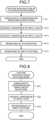
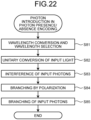
- FIG. 7 is a flowchart illustrating a method of photon introduction in the polarization encoding.
- the detection system 1 executes processing as illustrated in steps S11 to S15 in FIG. 7 .
- the connection of components implementing the function of each block may be implemented by a free space, an optical cable, or an optical circuit. Each block of the flowchart will be described below.
- a mechanism for selecting the wavelength of light may be introduced. Examples include implementation by a high pass filter (HPF), a low pass filter (LPF), or a band pass filter (BPF).
- HPF high pass filter
- LPF low pass filter
- BPF band pass filter
- the detection system 1 causes two photons interfered by the previous BS/PBS to be branched in a polarization state. Examples include implementation with PBS.
- the detection system 1 executes it.
- the photons branched by polarization are further branched or diffused to branch the input photons. Examples include an optical divider, a lens that diffuses light, or a combination thereof.
- FIG. 8 is a flowchart illustrating a method of photon introduction in the path encoding.
- the detection system 1A executes processing illustrated in steps S21 to S23 in FIG. 8 .
- the components that perform the functions of the blocks and the connections of the components are similar to the configurations described in ⁇ 1-5. Method for Implementing Photon Introduction in Polarization Encoding> unless otherwise specified. Each block of the flowchart will be described below.
- the detection system 1A performs unitary conversion in order to cause the two input light beams to interfere with each other at the BS.
- the mechanism for unitary conversion may be installed on either or both of the two optical paths.
- the detection system 1A causes two input light beams to interfere with each other by the two-input/two-output BS, and makes it impossible to determine from which input path the light beams have arrived.
- Examples include BSs that stochastically split light into two paths.
- FIG. 9 is a flowchart illustrating a method of light detection.
- the detection systems 1 and 1A execute processing illustrated in steps S31 to S37 in FIG. 9 .
- Each block of the flowchart will be described below.
- the detection systems 1 and 1A may perform wavelength conversion of the input light at any position before the light detection in order to increase the detection efficiency of the input light or to enable the input light to be detected.
- Examples include a method for converting light such as a communication wavelength band that cannot be detected by Si into a wavelength that can be detected by Si when the light receiving element of the photodetector is Si.
- As a method of wavelength conversion in this case there is SHG or SFG described in ⁇ 1-5. Method for Implementing Photon Introduction in Polarization Encoding>.
- the detection systems 1 and 1A introduce input light into a plurality of spatially separated elements of a photodetector. Examples include a method in which a plurality of optical fibers is melted or branched by a waveguide of an optical circuit.
- An isolation mechanism may be introduced so that crosstalk of input light does not occur between elements of the photodetector.
- An implementation method will be described later in ⁇ 1-8. Method for Implementing Isolation>.
- the detection systems 1 and 1A detect input light. At this time, the detection systems 1 and 1A may perform detection using a single photon detection unit or may perform detection using a photon number detection unit. Any of the detection units may be a detector including a plurality of light detection elements, or may be a detector system including a plurality of independent detectors.
- the detection systems 1 and 1A acquire a time at which light is detected. Examples include a method in which a common timing clock is used in all the photodetectors included in the detection systems 1 and 1A, and a time is obtained from a counter associated with the clock.
- the detection systems 1 and 1A output information of light detection to the signal processing device that performs the post-selection.
- Examples of the case of outputting information by a digital signal include a method of outputting a time at which light is detected and an address of an element as a data packet.
- Examples of the case of outputting information from an analog signal include a method of externally outputting intensity of a light reception signal of an element via an analog cable or the like in a form in which all the elements included in the detection systems 1 and 1A can be uniquely specified.
- FIG. 10 is a diagram illustrating a specific example of isolation.
- a structure in which a semiconductor substrate on which an avalanche photodiode element is formed is insulated and separated from other adjacent pixels is introduced. Note that reference numerals in the drawings mean the following.
- CMOS complementary metal oxide semiconductor
- 41 sensor substrate, 42: sensor-side wiring layer, 43: logic-side wiring layer, 51: N-well, 52: P-type diffusion layer, 53: N-type diffusion layer, 54: hole accumulation layer, 55: pinning layer, 56: high-concentration P-type diffusion layer, 57: avalanche multiplication region, 61: metal film, 62: insulating film, 63: interpixel separation unit, 71 to 73: contact electrode, 74 to 76: metal wiring, 77 to 79: contact electrode, 80 to 82: metal pad, 91 to 93: electrode pad, 94: insulating layer, 95 to 100: contact electrode, 101 to 103: metal pad electrode.
- CMOS complementary metal oxide semiconductor
- FIG. 13 is a flowchart illustrating a method of the post-selection. Each block of the flowchart will be described below.
- the detection systems 1 and 1A execute processing illustrated in steps S31 to S37 in FIG. 9 .
- the following processing is executed by a signal processing device (computer) included in the detection systems 1 and 1A.
- a signal processing device that performs the post-selection receives light detection information from a photodetector. Examples include a method of receiving a time at which light is detected by a digital signal and an address of an element as a data packet, and a method of receiving strength of an output signal in a form in which the element address can be specified by an analog signal.
- the signal processing device determines whether photons have been detected simultaneously (whether two photons have been detected within the time resolution of the detector).
- Examples of the case of receiving information of photon detection as a digital signal include a method of determining simultaneous detection from information of time of light detection included in a data packet.
- Examples of the case of receiving the information as an analog signal include a method of performing balance type measurement for calculating a difference between outputs of different elements in a signal processing device and determining simultaneous detection.
- the user of the simultaneous detection information is notified of the success of the simultaneous detection.
- Examples include a method of notifying an external device via the Internet, a local area network (LAN), or the like, and a method of notifying software in a signal processing device that performs the post-selection via an application program interface.
- a bell state is determined in order to form a quantum entanglement state.
- Examples of the implementation method include a method of determining which one of the four bell states is present from the address of the element that has detected light. Note that multiple entanglements such as a GZH state and a cluster state may be used as a variation of the quantum entanglement to be formed.
- the node in which the quantum entanglement is desired to be formed is notified of the determined bell state. Examples include notification to an external device via the Internet, a LAN, or the like.
- FIGS. 14 and 15 are diagrams illustrating modification examples of the photon detector (group) and the post-selection functional unit.
- the photon detector (group) and the post-selection functional unit may be mixedly mounted on the same chip, or may be divided and mounted on different chips and bonded.
- the photon detector (group) and the post-selection functional unit may be made into different packages and communicated. Further, communication may be performed among a plurality of photon detectors (groups). (For example, correction information, sharing of information regarding detection, and the like)
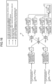
- FIG. 16 is a diagram illustrating an example of a configuration of the present embodiment in a case of the polarization encoding.
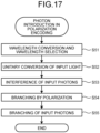
- FIG. 17 is a flowchart illustrating a method of photon introduction in the polarization encoding. Note that description of points similar to those described above will be omitted as appropriate.
- a first processing unit 2a and a second processing unit 3a corresponding to a path from a quantum entangled light source a and a first processing unit 2b and a second processing unit 3b corresponding to a path from a quantum entangled light source b are arranged before a beam splitter 4.
- first processing unit 2a the first processing unit 2b, and the like are not particularly distinguished, they are collectively referred to as a first processing unit 2.
- second processing unit 3a, the second processing unit 3b, and the like are not particularly distinguished, they are collectively referred to as a second processing unit 3.
- the detection system 1B includes the beam splitter 4, and the detection system 1B includes two polarizing beam splitters 5a and 5b, four light branching units 6a, 6b, 6c, and 6d, four photodetectors 7a, 7b, 7c, and 7d, and a post-selection 8.
- the polarizing beam splitters 5a and 5b and the like are not particularly distinguished, they are collectively referred to as a polarizing beam splitter 5.
- the light branching units 6a, 6b, 6c, 6d, and the like are not particularly distinguished, they are collectively referred to as a light branching unit 6.
- the photodetectors 7a, 7b, 7c, 7d, and the like are not particularly distinguished, they are collectively referred to as a photodetector 7.
- the type of the line to be connected between the components in FIG. 16 indicates a connection mode between the components.
- the connection corresponding to the solid line between the quantum entangled light sources a and b and the first processing unit 2 is implemented by an optical fiber.
- a solid line between the quantum entangled light sources a and b and the first processing unit 2 indicates that light from the light source is input (incident) to the detection system 1 by the optical fiber.
- the detection systems 1, 1A, and 1B, or the like is applied to quantum communication
- light from the quantum entangled light source is introduced into the system through an optical fiber. Note that, in a case where the detection systems 1, 1A, and 1B, and the like are not particularly distinguished, they are collectively referred to as a detection system 1.
- connection corresponding to the solid line between the quantum entangled light sources a and b and the first processing unit 2 is implemented by the optical fiber. Note that, in a case where the detection system 1B is applied to the quantum sensing described later, the connection corresponding to the solid line between the quantum entangled light sources a and b and the first processing unit 2 is implemented by either an optical fiber or a free space.
- connection corresponding to the dotted line between the first processing unit 2 and the photodetector 7 is implemented by any of an optical fiber, a waveguide in an optical circuit, and a free space.
- the path for transmitting light between the components in the detection system 1 may be any of an optical fiber, a waveguide in an optical circuit, and a free space.
- the detection system 1B executes processing as illustrated in steps S51 to S55.
- steps S51 to S55 In photon introduction in the polarization encoding, light in an overlapping state of two pulses illustrated below each light source in FIG. 16 , for example, is input from the two quantum entangled light sources a and b.
- step S53 the detection system 1B executes interference of input photons.
- step S53 corresponds to step S13 in FIG. 7 .
- the detection system 1B executes the processing of step S53 by the beam splitter 4.
- step S54 the detection system 1B executes branching by polarization (step S54).
- step S54 corresponds to step S14 in FIG. 7 .
- the detection system 1B executes the processing of step S54 by the polarizing beam splitter 5.
- the detection system 1B executes branching of the input photons (step S55).
- the detection system 1B further branches or diffuses the photons branched by the polarized light, and introduces the photons into the photodetector 7. Examples include an optical divider, a lens that diffuses light, or a combination thereof.
- the detection system 1B executes the processing of step S55 by the light branching unit 6.
- FIG. 18 is a diagram illustrating an example of a configuration of the present embodiment in a case of the path encoding.
- FIG. 19 is a flowchart illustrating a method of photon introduction in the path encoding. Note that description of points similar to those described above will be omitted as appropriate.
- a first processing unit 2a1 and a second processing unit 3a1 corresponding to a path a-1 from the quantum entangled light source a and a first processing unit 2b1 and a second processing unit 3b1 corresponding to a path b-1 from the quantum entangled light source b are arranged before a beam splitter 4a.
- a first processing unit 2a2 and a second processing unit 3a2 corresponding to a path a-2 from the quantum entangled light source a and a first processing unit 2b2 and a second processing unit 3b2 corresponding to a path b-2 from the quantum entangled light source b are arranged before a beam splitter 4b.
- first processing units 2a1, 2a2, 2b1, 2b2, and the like are not particularly distinguished, they are collectively referred to as a first processing unit 2, and in a case where the second processing units 3a1, 3a2, 3b1, 3b2, and the like are not particularly distinguished, they are collectively referred to as a second processing unit 3. Further, in a case where the beam splitters 4a and 4b and the like are not particularly distinguished, they are collectively referred to as a beam splitter 4.
- the detection system 1C illustrated in FIG. 18 includes the beam splitter 4, the photodetectors 7 provided corresponding to respective paths branched by the beam splitter 4 and the polarizing beam splitter 5, the plurality of light branching units 6 that branch light to be introduced into each of the plurality of photodetectors 7, and the post-selection 8 that detects respective detection timings of photons in the plurality of photodetectors 7.
- the detection system 1C executes wavelength conversion and wavelength selection (step S61).
- the processing of step S61 corresponds to step S21 in FIG. 7 .
- the detection system 1C executes the processing of step S61 by the first processing unit 2.
- the wavelength conversion and the wavelength selection are arbitrary processing, and may be executed or may not be executed as necessary.
- the detection system 1C executes unitary conversion of the input light (step S62).
- the processing of step S62 corresponds to step S22 in FIG. 7 .
- the detection system 1C executes the processing of step S62 by the second processing unit 3.
- the detection system 1C executes processing by the beam splitter (step S63).
- the detection system 1C performs interference of input photons.
- the processing of step S63 corresponds to step S23 in FIG. 7 .
- the detection system 1C executes the processing of step S63 by the beam splitter 4.
- FIG. 20 is a flowchart illustrating a method of the post-selection in a case of quantum communication. Note that description of points similar to those described above will be omitted as appropriate. Note that the processing illustrated in FIG. 20 may be performed by any detection system 1 such as the detection system 1B, 1C, or the like as long as the processing can be performed.
- the detection system 1 executes processing as illustrated in steps S71 to S74 in the post-selection in the quantum communication. For example, the detection system 1 executes processing as illustrated in steps S71 to S74 by the post-selection 8.
- the detection system 1 executes reception of the light detection information (step S71).
- the processing of step S71 corresponds to step S41 in FIG. 13 .
- step S72 the detection system 1 executes determination of simultaneous detection of photons.
- the processing of step S72 corresponds to step S42 in FIG. 13 .
- step S72: No the detection system 1 ends the post-selection processing without executing the processing of steps S73 and S74.
- Step S72 When it is determined that photons are simultaneously detected (Step S72: Yes), the detection system 1 executes processing of confirming the bell state (Step S73). The processing of step S73 corresponds to step S44 in FIG. 13 . Then, the detection system 1 executes notification of the bell state (step S74). The processing of step S74 corresponds to step S45 in FIG. 13 .
- the detection system 1 can improve the quantum entanglement generation rate by using the photodetectors 7 such as an arrayed detector, and can efficiently generate the quantum entanglement state.
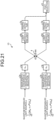
- the detection system 1D illustrated in FIG. 21 receives quantum entangled light from one or more paths.
- the detection system 1D has a configuration in which the polarizing beam splitter is removed from the detection system 1 illustrated in FIG. 5 , a light branching unit is arranged before each of the light detection units, and the processing unit for wavelength conversion + wavelength selection is arranged before the beam splitter.
- the first processing unit 2a and the second processing unit 3a corresponding to the path from the quantum entangled light source a and the first processing unit 2b and the second processing unit 3b corresponding to the path from the quantum entangled light source b are arranged before the beam splitter 4.
- the detection system 1D illustrated in FIG. 21 includes the beam splitter 4, the photodetectors 7 provided corresponding to respective paths branched by the beam splitter 4, the plurality of light branching units 6 that branch light to be introduced into each of the plurality of photodetectors 7, and the post-selection 8 that detects respective detection timings of photons in the plurality of photodetectors 7.
- the type of the line to be connected between the components in FIG. 21 indicates a connection mode between the components.
- the relationship between the connection modes of the types of lines is similar to that in FIG. 16 , and thus a detailed description thereof will be omitted.
- the connection corresponding to the solid line between the quantum entangled light sources a and b and the first processing unit 2 is implemented by either an optical fiber or a free space.
- the connection corresponding to the solid line between the quantum entangled light sources a and b and the first processing unit 2 is implemented by an optical fiber.
- the detection system 1D executes processing as illustrated in steps S81 to S85.
- steps S81 to S85 In photon introduction in the photon presence/absence encoding, light in an overlapping state of two pulses illustrated below each light source in FIG. 21 , for example, is input from the two quantum entangled light sources a and b.
- the detection system 1D executes wavelength conversion and wavelength selection (step S81).
- the processing of step S81 corresponds to step S11 in FIG. 7 .
- the detection system 1D executes the processing of step S81 by the first processing unit 2.
- the wavelength conversion and the wavelength selection are arbitrary processing, and may be executed or may not be executed as necessary.
- the detection system 1D executes unitary conversion of the input light (step S82).
- the processing of step S82 corresponds to step S12 in FIG. 7 .
- the detection system 1D executes the processing of step S82 by the second processing unit 3.
- the detection system 1D executes branching of the input photons (step S85).
- the detection system 1D further branches or diffuses the photons branched by the polarized light, and introduces the photons into the photodetector 7. Examples include an optical divider, a lens that diffuses light, or a combination thereof.
- the detection system 1D executes the processing of step S85 by the light branching unit 6.
- FIG. 23 is a diagram illustrating an example of a configuration of the present embodiment in a case of time encoding.
- FIG. 24 is a flowchart illustrating a method of photon introduction in the time encoding. Note that description of points similar to those described above will be omitted as appropriate.
- the detection system 1E illustrated in FIG. 23 receives quantum entangled light from one or more paths.
- the detection system 1E has a configuration in which the polarizing beam splitter is removed from the detection system 1 illustrated in FIG. 5 , a mirror and a phase modulator are added, a light branching unit is arranged before each of the light detection units, and a processing unit for wavelength conversion + wavelength selection is arranged before the beam splitter.
- the detection system 1E includes mirrors 9a and 9b and a phase modulator 20.
- the mirrors 9a and 9b and the like are not particularly distinguished, they are collectively referred to as a mirror 9.
- the mirror 9 is a mirror that reflects photons.
- the mirror 9 is arranged at a position where light from the beam splitter 4a is reflected and input to the beam splitter 4b.
- the phase modulator 20 performs phase modulation of one light beam branched by the beam splitter 4a.
- the phase modulator 20 is arranged in a path between the beam splitter 4a and the beam splitter 4b.
- the type of the line to be connected between the components in FIG. 23 indicates a connection mode between the components.
- the relationship between the connection modes of the types of lines is similar to that in FIG. 16 , and thus a detailed description thereof will be omitted.
- the connection corresponding to the solid line between the quantum entangled light sources a and b and the first processing unit 2 is implemented by either an optical fiber or a free space.
- the connection corresponding to the solid line between the quantum entangled light sources a and b and the first processing unit 2 is implemented by an optical fiber.
- FIGS. 16 , 18 , 21 , and 23 described above indicate connection modes between components, and the types of lines in other drawings (for example, FIG. 25 ) do not indicate connection modes between components.
- the detection system 1E executes processing as illustrated in steps S91 to S96. Note that the components that perform the functions of the blocks, the connections of the components, and the like are similar to those described in ⁇ 1-5. Method for Implementing Photon Introduction in Polarization Encoding> unless otherwise specified. Each block of the flowchart will be described below.
- E>b in Expression (2) represent temporally early pulses emitted from the quantum entangled light sources a and b, respectively,
- L>b in Expression (2) represent pulses emitted later than
- the detection system 1E executes wavelength conversion and wavelength selection (step S91).
- the wavelength conversion may be performed at any position in the flowchart illustrated in FIG. 24 .
- the wavelength after conversion may be both shorter and longer than the input light.
- a mechanism for selecting a wavelength of light to be input to the photodetector 7 after wavelength conversion may be introduced.
- the detection system 1E executes the processing of step S91 by the first processing unit 2.
- the detection system 1E executes processing by the beam splitter #2 (for example, the beam splitter 4b in FIG. 23 ) (step S95).
- the detection system 1E multiplexes the light beams branched by the beam splitter #1.
- the detection system 1E executes the processing of step S95 by the beam splitter 4b.
- the multiplexed light is in an overlapping state as illustrated in the following Expression (4).
- FIG. 25 is a diagram illustrating an example of a configuration of the present embodiment of the quantum sensing.
- a light detection system applied to the quantum sensing is referred to as a sensing system.
- the sensing system may be rephrased as a measurement device or the like.
- the sensing system 10 illustrated in FIG. 25 includes a quantum entanglement generator 1F and a quantum entangled light source 30 that outputs at least two photons in a quantum entanglement state.
- the quantum entanglement generator 1F illustrated in FIG. 25 is merely an example of the configuration of the quantum entanglement generator, and any configuration can be employed as the quantum entanglement generator as long as desired sensing can be performed.
- the detection system 1 such as the detection system 1 to 1E described above may be used as the quantum entanglement generator of the sensing system 10.
- the quantum entanglement generator 1F detects a photon detection timing by the photodetector 7 provided corresponding to the path branched by the at least one beam splitter 4 that causes interference of the quantum entangled light.
- a quantum entanglement generator 1F illustrated in FIG. 25 includes the photodetectors 7 provided corresponding to respective paths branched by the beam splitter 4 and the polarizing beam splitters 5a and 5b, the light branching unit 6 that branches light to be introduced into the plurality of photodetectors 7, and the post-selection 8 that detects respective detection timings of photons in the plurality of photodetectors 7.
- first processing units 2a1, 2a2, 2b1, 2b2, and the like are not particularly distinguished, the first processing units 2a1, 2a2, 2b1, 2b2, and the like are collectively referred to as a first processing unit 2.
- the first processing unit 2 executes processing on the quantum entangled light after the interference by the beam splitter 4.
- the first processing unit 2 executes at least one processing of wavelength conversion or wavelength selection on the quantum entangled light after interference by the beam splitter 4.
- the quantum entanglement generator 1F receives light from the second light guide path LP2 and the third light guide path LP3.
- the sensing system 10 illustrated in FIG. 25 includes a sum frequency generator 40.
- the sum frequency generator 40 is arranged in at least one of the second light guide path LP2 or the third light guide path LP3. In FIG. 25 , the sum frequency generator 40 is arranged in the third light guide path LP3.
- the sum frequency generator 40 executes processing related to sum frequency generation.
- the sum frequency generator 40 is used to equalize energy of two photons entering the BS.
- a periodically inverted polarized LiNbO crystal or the like may be used for the sum frequency generator 40.
- the sum frequency generator 40 converts two input light beams into one output light beam by a nonlinear optical effect. In this case, for example, the frequency of the output light of the sum frequency generator 40 is a total value of the input light.
- the sensing system 10 implements sensing for detecting reflected light from a target.
- the sensing system 10 provides a method for two-photon quantum interference in sensing using a photon pair in a quantum entanglement state.
- the sensing system 10 projects one of the quantum entangled light pair onto the target, and detects the reflected or scattered photon and the other of the photon pair by two-photon quantum interference, thereby implementing highly sensitive sensing.
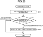
- FIG. 26 is a flowchart illustrating a method of the post-selection in a case of the quantum sensing. Note that description of points similar to those described above will be omitted as appropriate. Note that the processing illustrated in FIG. 26 may be performed by the detection systems 1 and 10 or the like as long as the processing can be performed.
- the sensing system 10 executes processing as illustrated in steps S101 to S103 in the post-selection in the quantum sensing. For example, the sensing system 10 executes processing as illustrated in steps S101 to S103 by the post-selection 8. The sensing system 10 executes reception of the light detection information (step S101). The processing of step S101 corresponds to step S41 in FIG. 13 .
- step S102 When it is determined that photons are simultaneously detected (step S102: Yes), the sensing system 10 executes notification of simultaneous detection (step S103).
- the processing of step S103 corresponds to step S46 in FIG. 13 .
- the quantum sensing by the sensing system 10 may be applied to any sensing.
- the quantum sensing by the sensing system 10 may be applied to sensing targeting a fluorescent substance.
- the quantum sensing by the sensing system 10 may be applied to sample analysis.
- the quantum sensing by the sensing system 10 may be applied to single pixel imaging.
- the quantum sensing by the sensing system 10 may be applied to an imaging system.
- first to fourth application examples specific examples of application of the sensing system as described above to the quantum sensing will be described as first to fourth application examples.
- the first to fourth application examples described below are merely examples, and the sensing system may be applied to any sensing as long as the sensing system is applicable.
- sensing systems 10A to 10D and the like described below are not particularly distinguished, they are collectively referred to as a sensing system 10.
- FIG. 27 is a diagram illustrating the first application example of the quantum sensing.
- the sensing system 10A illustrated in FIG. 27 includes a quantum entanglement generator 1G, the quantum entangled light source 30, an excitation light source 35, and a lens unit 65.
- the excitation light source 35 outputs excitation light to an observation target TG1.
- the excitation light source 35 irradiates the observation target TG1 with target excitation light having a frequency ⁇ 2.
- the lens unit 65 scans the observation target TG1 which is a target.
- the observation target TG1 is an up-conversion probe, a tissue having a structure serving as a harmonic source, or the like.
- a band pass filter 50a is arranged in the second light guide path LP2, and in addition to the sum frequency generator 40, a phase adjuster 25 and a band pass filter 50b are arranged in the third light guide path LP3. Note that, in a case where the band pass filters 50a and 50b and the like described below are not particularly distinguished, they are collectively referred to as a band pass filter 50.
- the band pass filter 50 is arranged in at least one of the second light guide path LP2 or the third light guide path LP3, functions as a band pass filter (BPF), and executes processing related to frequency.
- the phase adjuster 25 is arranged in at least one of the second light guide path or the third light guide path. The phase adjuster 25 executes processing related to phase adjustment. Further, in FIG. 27 , idler excitation light having a frequency f2 is input to the sum frequency generator 40.
- the sensing system 10A provides a method for measuring a specific fluorescent substance with high sensitivity.
- the sensing system 10A performs an operation corresponding to the above change on the other of the photon pair and detects both photons by two-photon quantum interference, thereby implementing highly sensitive sensing.
- the sensing system 10A irradiates the observation target TG1 such as a tissue or a cell including a target (imaging target) with photons having a frequency ⁇ 1 from the quantum entangled light source 30.
- the observation target TG1 is irradiated with target excitation light having a frequency ⁇ 2 from another light source.
- the sensing system 10A transmits only the light having the frequency F by passing the light received from the observation target TG1 through the band pass filter 50 (BPF).
- BPF band pass filter 50
- the BPF transmitted light is introduced into the beam splitter 4 (BS).
- another light (idler light) from the quantum entangled light source 30 is introduced into the beam splitter 4 (BS).
- the sensing system 10A may optionally perform phase adjustment for performing simultaneous measurement with fluorescence by the phase adjuster 25.
- the sensing system 10A may perform the sum frequency generation by the sum frequency generator 40 using the idler excitation light in order to match the frequency of the idler light with the frequency F of the fluorescence. Note that the phase adjustment and the sum frequency generation may be optionally exchanged.
- two beams of light simultaneously introduced into the BS generate two-photon interference, are then branched by the polarization characteristic in the polarizing beam splitter 5 (PBS), and are further diffused into a sensitive region of the photodetector 7 by the light branching unit 6 and measured.
- PBS polarizing beam splitter 5
- simultaneous measurement of the measured signals is determined by the post-selection 8, and only valid measurement events are selected.
- the sensing system 10A as described above may be applied to a two-photon excitation microscope for microstructural analysis of biological tissues (such as the brain).
- the sensing system 10A may be applied to a second harmonic microscope for pathological tissue diagnosis and early diagnosis by cancer fibrosis detection.
- the sensing system 10A allows for long term target observation with reduced toxicity and allows for reduced toxicity with reduced phototoxicity and reduced probe dosage. Further, the sensing system 10A can acquire information in a depth direction (about 10 mm) of a thick sample as compared with the existing sample (up to about 2 mm) .
- FIG. 28 is a diagram illustrating the second application example of the quantum sensing. Note that description of points similar to those described above will be omitted as appropriate.
- the quantum entanglement generator 1H has a configuration in which the arrangement of the sum frequency generator 40 is changed from the third light guide path LP3 to the second light guide path LP2 in the quantum entanglement generator 1G illustrated in FIG. 27 .
- excitation light having a frequency ⁇ 2 is input to the sum frequency generator 40.
- the sensing system 10B is a system that performs measurement while scanning (alternatively, move target) a target (for example, a cell, a tissue, or the like) and performs imaging on the basis of a measurement result.
- a target for example, a cell, a tissue, or the like
- the sensing system 10B may perform frequency conversion by sum frequency generation in the sum frequency generator 40.
- the sensing system 10B transmits only the light having the converted frequency F by passing the photons after conversion through the band pass filter 50 (BPF).
- BPF band pass filter 50
- the light transmitted through the BPF is introduced into the beam splitter 4 (BS).
- BS beam splitter 4
- another light (idler light) from the quantum entangled light source 30 is introduced into the BS.
- the phase adjustment for performing the simultaneous measurement with the fluorescence may be optionally performed by the phase adjuster 25.
- FIG. 29 is a diagram illustrating the third application example of the quantum sensing. Note that description of points similar to those described above will be omitted as appropriate.
- the sensing system 10C illustrated in FIG. 29 includes a quantum entanglement generator 1I, the quantum entangled light source 30, and a light receiving probe 66.
- the light receiving probe 66 is a probe for receiving light from an observation target TG3 which is a target.
- the observation target TG3 is a cerebral blood flow, a fluorescent probe, or the like.
- the quantum entanglement generator 1I has a configuration in which the arrangement of the phase adjuster 25 and the sum frequency generator 40 is changed from the third light guide path LP3 to the third light guide path LP2 in the quantum entanglement generator 1G illustrated in FIG. 27 .
- signal excitation light is input to the sum frequency generator 40.
- the sensing system 10C irradiates the head with photons from the quantum entangled light source 30 through an optical fiber (transmission optical fiber).
- An assumed target includes the following, and light received by the sensing system 10C differs depending on a difference in the observation target TG3.
- the light received by the sensing system 10C is reflected light from the cerebral blood flow.
- the light received by the sensing system 10C is fluorescent light from the probe.
- the light emitted from the observation target TG3 is introduced into the quantum entanglement generator 1I of the sensing system 10C through the light receiving probe 66.
- the sensing system 10C introduces the received light into the beam splitter 4 (BS) for simultaneous measurement with the idler light from the quantum entangled light source 30.
- phase adjustment may be optionally performed by the phase adjuster 25.
- the sensing system 10C may perform frequency conversion by sum frequency generation in order to match the frequencies of the received light and the idler light. When the frequency conversion is performed, the sensing system 10C passes the light after conversion through the band pass filter 50 (BPF) in order to select the light of which the sum frequency is successful.
- BPF band pass filter 50
- the other light emitted from the quantum entangled light source 30 is introduced into the BS in order to interfere with the light emitted from the observation target TG3.
- two beams of light simultaneously introduced into the BS generate two-photon interference, are then branched by the polarization characteristic in the polarizing beam splitter 5 (PBS), and are further diffused into the sensitive region of the photodetector 7 by the light branching unit 6 and measured.
- simultaneous measurement of the measured signals is determined by the post-selection 8, and only valid measurement events are selected.
- the sensing system 10C as described above may be applied to rehabilitation effect determination and pain evaluation by evaluation of the brain activity amount/brain activation site. Further, the sensing system 10C may be applied to medical diagnosis of dementia, brain tumor, and the like. Furthermore, the sensing system 10C may be applied to a brain-machine interface (Brain-machine I/F).
- Brain-machine I/F brain-machine interface
- the sensing system 10C enables medical diagnosis by using a near-infrared fluorescent probe.
- the sensing system 10C can acquire information in a deeper depth direction (about 40 mm) than existing systems (up to about 20 mm).
- the sensing system 10C can measure a site (white matter, cerebellum, or the like) different from the conventional site.
- the sensing system 10D illustrated in FIG. 30 includes a quantum entanglement generator 1J, the quantum entangled light source 30, a pulsed light source 36, an image sensor 85, and an image processing unit 86.
- the pulsed light source 36 irradiates an observation target TG4 as a target with light.
- the observation target TG4 is a cell flowing in a fluid in an analysis sample or the like in the in vitro diagnosis.
- the quantum entanglement generator 1J has a configuration in which the arrangement of the sum frequency generator 40 is changed from the third light guide path LP3 to the fourth light guide path LP2 in the quantum entanglement generator 1G illustrated in FIG. 27 . Further, in FIG. 30 , signal excitation light is input to the sum frequency generator 40.
- the sensing system 10D is a system for detecting a trace target in a sample that is difficult to detect by an existing analysis method.
- two beams of light simultaneously introduced into the BS generate two-photon interference, are then branched by the polarization characteristic in the polarizing beam splitter 5 (PBS), and are further diffused into the sensitive region of the photodetector 7 by the light branching unit 6 and measured.
- PBS polarizing beam splitter 5
- simultaneous measurement of the measured signals is determined by the post-selection 8, and only valid measurement events are selected.
- the sensing system 10D can directly measure fluorescence emitted from an intracellular organ, thereby enabling non-fluorescence/non-staining measurement, fluorescence measurement of a near infrared (NIR) region, and the like.
- NIR near infrared
- the sensing system 10 can implement high-sensitivity sensing by selectively measuring a signal, and can efficiently generate a quantum entanglement state.
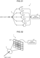
- FIG. 31 is a diagram illustrating a first configuration example of the light branching unit and the photodetector.
- FIG. 31 corresponds to the portion of the configuration PT1 of the portion in FIG. 16 .
- FIG. 31 illustrates an outline of configurations of portions of the light branching unit 6d, the photodetectors 7d of the four photodetectors 7, and the post-selection 8 among the four light branching units 6 in FIG. 16 .
- the first configuration example there is a device that issues a timing clock to the outside of a detector (for example, the detection unit 70), and time synchronization is performed between the detectors.
- a means for synchronizing time between the detectors a means other than those described above may be applied.
- a function that requires advance preparation such as training and calibration before measurement may be introduced.
- a detector capable of detecting a single photon or the number of photons may be used.
- a function such as cooling or variable bias for improving and changing characteristics of the detector may be provided.
- the photodetector 7 is an array element.
- the photodetector 7 includes a plurality of regions AR (for example, light receiving elements) on a light receiving surface of the array element as a plurality of detection units.
- the photodetector 7 has 16 regions AR.
- the light branching unit 6 is a lens that branches and introduces light into each of the plurality of regions of the array element. In FIG. 32 , the light branching unit 6 branches light into each of the plurality of regions AR of the photodetector 7.
- the light branching unit 6 that is a lens disperses and introduces light into the photodetector 7 that is an array element.
- the photodetector 7 that is an array element.
- a single array type detector is used as the photodetector 7.
- the input light is diffused on the light receiving surface of the photodetector 7 which is an array type detector by diffusion at a lens or by the light branching unit 6 which is an optical divider.
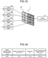
- FIG. 33 is a diagram illustrating another configuration example of the photodetector.
- FIG. 33 illustrates an example of a method for implementing the photodetector 7.
- all the photodetectors may be configured using a single array type detector as the photodetector 7.
- the detection system 1 may be a system having one photodetector 7.
- the photodetector 7 is an array element.
- the photodetector 7 includes a plurality of regions AR (for example, light receiving elements) on a light receiving surface of the array element as a plurality of detection units.
- the photodetector 7 has 16 regions AR.
- the photodetector 7 is configured so that four regions AR on the upper left side detect light from the light branching unit 6a, four regions AR on the upper right side detect light from the light branching unit 6b, four regions AR on the lower left side detect light from the light branching unit 6c, and four regions AR on the lower right side detect light from the light branching unit 6d.
- the photodetector 7 may be used as an array type detector that allocates a plurality of light detection elements to each of the paths.
- the photodetector 7 which is a single array type detector, is used to perform all light detection necessary for the detection system 1 and the like.
- FIG. 34 is a diagram illustrating an example of photodetector performance in a single element.
- FIG. 34 illustrates, as an example, light detection efficiency, a dark count rate, a Deadtime, the light detection time width, and the like as indices indicating the performance of the assumed photodetector single element.
- T DT that is a deadtime at which light detection cannot be performed for a while occurs.
- PPMT photomultiplier tube
- SPAD superconducting single photon detector
- SSPD superconducting single photon detector
- TES transition edge sensor
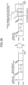
- FIG. 36 light can be detected when a time exceeding T DT has elapsed from the previous light detection.
- FIG. 36 is a diagram illustrating an example of a case where light can be detected.
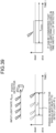
- FIG. 37 when the elapsed time from the previous light detection is within T DT , light cannot be detected.
- FIG. 37 is a diagram illustrating an example of a case where light cannot be detected.
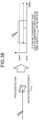
- FIG. 38 is a diagram illustrating an example of the model of light detection.
- the light detection time of the detector has a width T window , and thus, even if one photon reacts with the detector at a specific time, it is not possible to specify where in the T window the reaction occurs. Accordingly, it is considered that the light is uniformly diffused in the T window .
- An instantaneous rate R impulse of light at this time is assumed. When it is assumed that one photon is uniformly diffused in a T window of time, the rate R impulse of light in the T window is expressed by the following Expression (7).
- R impulse 1 T window
- the detection probability of light is obtained as a probability that light detection occurs when the detector is exposed to R impulse for a time T as in the following Expression (8).
- P T 1 ⁇ exp ⁇ PDE R impulse + R DCR T
- R DCR is a dark count rate at which the photodetector reacts without input of light.
- FIGS. 40 and 31 light input to the SPAD is diffused by the number of SPADs constituting the photodetector.
- FIG. 40 is a diagram illustrating an example of a model of light detection in a case where the photodetector includes multiple elements.
- FIG. 41 is a diagram illustrating an example of a model of light detection in a case where the photodetector includes multiple elements.
- FIG. 42 is a diagram illustrating an example of dispersed light and detection by multiple elements.
- the maximum light detection rate with respect to the number of elements is calculated.
- the maximum light detection rate is calculated in the following two steps (Step#1 and Step#2).
- Step#1 the term (R max pulse ) on the left side of Expression (16) that maximizes the light detection rate is calculated by the Newton method or the like using the following Expression (16).
- R pulse max argmax R pulse
- R pulse P meas N SPAD R pulse
- Step#2 an expected value of the light detection rate in a case where the term (R max pulse ) on the left side of Expression (16) is input to the photodetector is obtained as the maximum light detection rate R max as in the following Expression (17).
- R max R pulse max P meas N SPAD R pulse max
- FIGS. 43 and 44 are diagrams illustrating an example of calculation of the maximum light detection rate with respect to the number of elements.
- FIG. 43 is a diagram illustrating an example of calculation of the maximum light detection rate with respect to the number of elements in the form of a table.
- FIG. 44 is a diagram illustrating an example of calculation of the maximum light detection rate with respect to the number of elements in the form of a graph.
- the maximum detection rate increases substantially in proportion to the number of elements.
- the rate is derived by the calculation as described above, and based on this index, it can be seen that the performance is improved by increasing the number of detectors.
- a program for executing the above-described operation is stored and distributed in a computer-readable recording medium such as an optical disk, a semiconductor memory, a magnetic tape, or a flexible disk. Then, for example, by installing the program in a computer and executing the above-described processing, the control device can be configured.
- the control device may be a device (for example, a personal computer) outside the detection system 1, the sensing system 10, and the like (measurement device).
- the control device may be a device (for example, a processor) inside the detection system 1, the sensing system 10, and the like (measurement device).
- the present embodiment can be implemented as any configuration constituting a device or a system, for example, a processor as a system large scale integration (LSI) or the like, a module using a plurality of processors or the like, a unit using a plurality of modules or the like, a set obtained by further adding other functions to a unit, or the like (that is, a configuration of a part of the device).
- LSI system large scale integration
- the system means a set of a plurality of components (devices, modules (parts), and the like), and it does not matter whether or not all the components are in the same housing. Therefore, a plurality of devices housed in separate housings and connected via a network and one device in which a plurality of modules is housed in one housing are both systems.
- the detection system is a system that receives quantum entangled light from a plurality of paths.
- a detection system includes a plurality of beam splitters that cause interference of the quantum entangled light, light receiving elements provided corresponding to respective paths branched by the beam splitter, and a measurement instrument that detects respective detection timings of photons in the plurality of light receiving elements.
- the detection system is a system that receives quantum entangled light.
- a detection system includes a beam splitter that causes interference of the quantum entangled light, a plurality of polarizing beam splitters that branches, in a polarization state, the quantum entangled light after the interference by the beam splitter, light receiving elements provided corresponding to respective paths branched by the polarizing beam splitter, and a measurement instrument that detects respective detection timings of photons in the plurality of light receiving elements.
- the sensing system is a system that receives quantum entangled light from one or more paths.
- a detection system includes one or more beam splitters that cause interference of the quantum entangled light, light receiving elements provided corresponding to respective paths branched by a plurality of splitters including at least the beam splitter, a branching unit that branches light to be introduced into the plurality of light receiving elements, and a measurement instrument that detects respective detection timings of photons in the plurality of light receiving elements.
- a sensing system includes a quantum entangled light source that outputs at least two photons in a quantum entanglement state, and a quantum entanglement generator that detects a detection timing of a photon by a light receiving element provided corresponding to a path branched by at least one beam splitter that causes interference of the quantum entangled light.
- the quantum entanglement generator receives light from the second light guide path and the third light guide path.
- the number of times of quantum entanglement trials per unit time can be increased, so that the efficiency of quantum entanglement formation per unit time can be improved.
- the measurement device in the embodiment, the detection system 1 or the like
- the measurement device is a measurement device that receives quantum entangled light from one or more paths, and includes one or more beam splitters (in the embodiment, the beam splitter 4 or the like.
- the measurement device in the embodiment, the detection system 1 or the like
- the measurement device is a measurement device that receives quantum entangled light from a plurality of paths, and includes a plurality of beam splitters that cause interference of the quantum entangled light, light receiving elements provided corresponding to respective paths branched by the beam splitter, and a measurement instrument that detects respective detection timings of photons in the plurality of light receiving elements.
- the measurement device detects respective detection timings of photons in the light receiving elements provided corresponding to the paths branched by the plurality of beam splitters that cause interference of the quantum entangled light, and thereby can generate the quantum entanglement and perform detection by a simple configuration. Therefore, the measurement device can enable efficient generation of the quantum entanglement.
- a measurement device in the embodiment, the detection system 1A or the like is a measurement device that receives quantum entangled light, and includes a beam splitter that causes interference of the quantum entangled light, a plurality of polarizing beam splitters that branches, in a polarization state, the quantum entangled light after the interference by the beam splitter, light receiving elements provided corresponding to respective paths branched by the polarizing beam splitter, and a measurement instrument that detects respective detection timings of photons in the plurality of light receiving elements.
- the measurement device branches light to be introduced into the light receiving elements provided corresponding to the paths branched by the plurality of splitters including the beam splitter that causes interference of the quantum entangled light, and detects respective detection timings of photons in the light receiving elements, and thereby can generate the quantum entanglement and perform detection by a simple configuration. Therefore, the measurement device can enable efficient generation of the quantum entanglement.
- the measurement device includes a preprocessing unit (in the embodiment, the first processing unit 2, the second processing unit 3, and the like. The same applies hereinafter) that executes processing on the quantum entangled light before branching by the beam splitter.
- a preprocessing unit in the embodiment, the first processing unit 2, the second processing unit 3, and the like. The same applies hereinafter) that executes processing on the quantum entangled light before branching by the beam splitter.
- the preprocessing unit executes at least one processing of wavelength conversion, wavelength selection, or unitary conversion on the quantum entangled light.
- the measurement device executes at least one processing of wavelength conversion, wavelength selection, or unitary conversion on the quantum entangled light, and thereby can generate the quantum entanglement and perform detection by appropriate processing. Therefore, the measurement device can enable efficient generation of the quantum entanglement.
- the measurement device includes a postprocessing unit (in the embodiment, the first processing unit 2 or the like. The same applies hereinafter) that executes processing on the quantum entangled light after the interference by the beam splitter after the branching by the beam splitter.
- a postprocessing unit in the embodiment, the first processing unit 2 or the like. The same applies hereinafter) that executes processing on the quantum entangled light after the interference by the beam splitter after the branching by the beam splitter.
- the postprocessing unit executes at least one processing of wavelength conversion or wavelength selection on the quantum entangled light after interference by the beam splitter.
- the plurality of detection units is a plurality of elements that detects light branched by the branching unit.
- the measurement device detects respective detection timings of photons in the plurality of elements that detects light branched by the branching unit, and thereby can appropriately perform detection.
- branching unit is an optical divider that branches and introduces light into each of the plurality of elements.
- the light receiving element is an array element
- the plurality of detection units is a plurality of regions of a light receiving surface of the array element.
- the measurement device detects respective detection timings of photons in the plurality of regions of a light receiving surface of the array element, and thereby can appropriately perform detection.
- the branching unit is an optical member that branches and introduces light into each of the plurality of regions of the array element.
- the measurement device detects respective detection timings of photons in the plurality of detection units that detects light branched by the optical member that branches and introduces light into each of the plurality of regions of the array element, and thereby can appropriately perform detection.
- the measurement device in the embodiment, the sensing system 10 or the like
- the measurement device includes a quantum entangled light source (in the embodiment, the quantum entangled light source 30 or the like) that outputs at least two photons in a quantum entanglement state, and a quantum entanglement generator (in the embodiment, the quantum entanglement generator 1F or the like.
- the quantum entanglement generator receives light from the second light guide path and the third light guide path.
- the measurement device includes a sum frequency generation unit (in the embodiment, the sum frequency generator 40 or the like. The same applies hereinafter) arranged in at least one of the second light guide path or the third light guide path.
- a sum frequency generation unit in the embodiment, the sum frequency generator 40 or the like. The same applies hereinafter
- the measurement device executes processing related to a frequency in at least one path of the second light guide path or the third light guide path, and thereby can appropriately perform detection.
- the measurement device includes an excitation light source (in the embodiment, the excitation light source 35 or the like. The same applies hereinafter) that outputs excitation light to the observation target.
- an excitation light source in the embodiment, the excitation light source 35 or the like. The same applies hereinafter
- the quantum entanglement generator includes one or more beam splitters that cause interference of the quantum entangled light, light receiving elements provided corresponding to respective paths branched by a plurality of splitters including at least the beam splitter, and a measurement instrument that detects respective detection timings of photons in the plurality of light receiving elements.
- the measurement device detects respective detection timings of photons in the light receiving elements provided corresponding to the paths branched by the plurality of splitters including the beam splitter that causes interference of the quantum entangled light, and thereby can generate the quantum entanglement and perform detection by a simple configuration. Therefore, the measurement device can enable efficient generation of the quantum entanglement.
- the measurement device branches light to be introduced into the light receiving elements provided corresponding to the paths branched by the plurality of splitters including the beam splitter that causes interference of the quantum entangled light, and detects respective detection timings of photons in the light receiving elements, and thereby can generate the quantum entanglement and perform detection by a simple configuration. Therefore, the measurement device can enable efficient generation of the quantum entanglement.
- FIG. 45 is a hardware configuration diagram illustrating an example of a computer that implements functions of the information processing device.
- the computer 1000 includes a CPU 1100, a RAM 1200, a read only memory (ROM) 1300, a hard disk drive (HDD) 1400, a communication interface 1500, and an input-output interface 1600.
- Each unit of the computer 1000 is connected by a bus 1050.
- the CPU 1100 operates on the basis of a program stored in the ROM 1300 or the HDD 1400, and controls each unit. For example, the CPU 1100 develops a program stored in the ROM 1300 or the HDD 1400 in the RAM 1200, and executes processing corresponding to various programs.
- the ROM 1300 stores a boot program such as a basic input output system (BIOS) executed by the CPU 1100 when the computer 1000 is activated, a program depending on hardware of the computer 1000, and the like.
- BIOS basic input output system
- the HDD 1400 is a computer-readable recording medium that non-transiently records a program executed by the CPU 1100, data used by such a program, and the like.
- the HDD 1400 is a recording medium that records an information processing program according to the present disclosure as an example of program data 1450.
- the communication interface 1500 is an interface for the computer 1000 to connect to an external network 1550 (for example, the Internet).
- the CPU 1100 receives data from another device or transmits data generated by the CPU 1100 to another device via the communication interface 1500.
- the input-output interface 1600 is an interface for connecting an input-output device 1650 and the computer 1000.
- the CPU 1100 receives data from an input device such as a keyboard and a mouse via the input-output interface 1600. Further, the CPU 1100 transmits data to an output device such as a display, a speaker, or a printer via the input-output interface 1600.
- the input-output interface 1600 may function as a media interface that reads a program or the like recorded in a predetermined recording medium.
- the CPU 1100 of the computer 1000 executes an information processing program loaded on the RAM 1200 to implement a function of a control unit or the like of the control device.
- the HDD 1400 stores an information processing program according to the present disclosure and data in a storage unit of the control device. Note that the CPU 1100 reads the program data 1450 from the HDD 1400 and executes the program data 1450, but as another example, these programs may be acquired from another device via the external network 1550.
Landscapes
- Physics & Mathematics (AREA)
- General Physics & Mathematics (AREA)
- Spectroscopy & Molecular Physics (AREA)
- Optics & Photonics (AREA)
- Electromagnetism (AREA)
- Engineering & Computer Science (AREA)
- Computer Networks & Wireless Communication (AREA)
- Signal Processing (AREA)
- Photometry And Measurement Of Optical Pulse Characteristics (AREA)
Applications Claiming Priority (2)
| Application Number | Priority Date | Filing Date | Title |
|---|---|---|---|
| JP2022088259 | 2022-05-31 | ||
| PCT/JP2023/013509 WO2023233792A1 (fr) | 2022-05-31 | 2023-03-31 | Dispositif de mesure |
Publications (2)
| Publication Number | Publication Date |
|---|---|
| EP4535689A1 true EP4535689A1 (fr) | 2025-04-09 |
| EP4535689A4 EP4535689A4 (fr) | 2025-12-17 |
Family
ID=89026179
Family Applications (1)
| Application Number | Title | Priority Date | Filing Date |
|---|---|---|---|
| EP23815554.3A Pending EP4535689A4 (fr) | 2022-05-31 | 2023-03-31 | Dispositif de mesure |
Country Status (5)
| Country | Link |
|---|---|
| US (1) | US20250297890A1 (fr) |
| EP (1) | EP4535689A4 (fr) |
| JP (1) | JPWO2023233792A1 (fr) |
| CN (1) | CN119256505A (fr) |
| WO (1) | WO2023233792A1 (fr) |
Family Cites Families (6)
| Publication number | Priority date | Publication date | Assignee | Title |
|---|---|---|---|---|
| JP2012004956A (ja) | 2010-06-18 | 2012-01-05 | Nippon Telegr & Teleph Corp <Ntt> | 量子通信システム |
| GB2502264B (en) * | 2012-05-16 | 2014-07-02 | Toshiba Res Europ Ltd | A system and method for quantum teleportation |
| US9413470B1 (en) * | 2015-03-09 | 2016-08-09 | The Boeing Company | Electronic quantum information probability transfer |
| CN109586907B (zh) * | 2018-12-30 | 2022-03-15 | 广东尤科泊得科技发展有限公司 | 一种量子通信与量子时频传输的融合网络系统与方法 |
| EP4176295A4 (fr) * | 2020-07-01 | 2024-07-24 | Psiquantum Corp. | Multiplexage de trame dans des circuits photoniques |
| US11268806B2 (en) * | 2020-07-22 | 2022-03-08 | Honeywell International Inc. | Dynamical locking of optical path times using entangled photons |
-
2023
- 2023-03-31 EP EP23815554.3A patent/EP4535689A4/fr active Pending
- 2023-03-31 JP JP2024524199A patent/JPWO2023233792A1/ja active Pending
- 2023-03-31 CN CN202380042129.6A patent/CN119256505A/zh active Pending
- 2023-03-31 WO PCT/JP2023/013509 patent/WO2023233792A1/fr not_active Ceased
- 2023-03-31 US US18/862,803 patent/US20250297890A1/en active Pending
Also Published As
| Publication number | Publication date |
|---|---|
| WO2023233792A1 (fr) | 2023-12-07 |
| JPWO2023233792A1 (fr) | 2023-12-07 |
| CN119256505A (zh) | 2025-01-03 |
| EP4535689A4 (fr) | 2025-12-17 |
| US20250297890A1 (en) | 2025-09-25 |
Similar Documents
| Publication | Publication Date | Title |
|---|---|---|
| Bowman et al. | Wide-field fluorescence lifetime imaging of neuron spiking and subthreshold activity in vivo | |
| Liu et al. | Fast fluorescence lifetime imaging techniques: A review on challenge and development | |
| Wang et al. | Fast Wide‐Field Quantum Sensor Based on Solid‐State Spins Integrated with a SPAD Array | |
| CA2007776C (fr) | Spectrophotometrie a modulation de phase | |
| US11480514B2 (en) | Fluorescence lifetime imaging (FLIM) and flow cytometry applications for a time synchronized sensor network | |
| US20100027018A1 (en) | Device and method for acquiring image data from a turbid medium | |
| KR101209230B1 (ko) | 형광수명 측정 장치 및 방법 | |
| Nissilä et al. | Instrumentation for the accurate measurement of phase and amplitude in optical tomography | |
| US20230006677A1 (en) | Positron emission tomography system with a time synchronized network | |
| Stockton et al. | Single pixel quantitative phase imaging with spatial frequency projections | |
| Ferocino et al. | High throughput detection chain for time domain optical mammography | |
| Huang et al. | Interferometric speckle visibility spectroscopy (iSVS) for measuring decorrelation time and dynamics of moving samples with enhanced signal-to-noise ratio and relaxed reference requirements | |
| Tewson et al. | A multiplexed fluorescent assay for independent second-messenger systems: decoding GPCR activation in living cells | |
| Xia et al. | Click-free imaging of carbohydrate trafficking in live cells using an azido photothermal probe | |
| US20140285803A1 (en) | System and method of analysis by determining a depolarizing or dichroic character of an object | |
| EP4535689A1 (fr) | Dispositif de mesure | |
| Chiarelli et al. | Characterization of a fiber-less, multichannel optical probe for continuous wave functional near-infrared spectroscopy based on silicon photomultipliers detectors: in-vivo assessment of primary sensorimotor response | |
| Liu et al. | Quantum-enhanced microscopic imaging technology | |
| Hayakawa et al. | Demonstration of simultaneous optical transition-edge sensors readout using microwave SQUID multiplexer with 5 MHz flux ramp modulation | |
| Lagarto et al. | Development of low-cost instrumentation for single point autofluorescence lifetime measurements | |
| Pani et al. | Effects of multi-photon states in the calibration of single-photon detectors based on a portable bi-photon source | |
| Fiurášek | Fundamental limits on determination of photon number statistics from measurements with multiplexed on/off detectors | |
| US8946656B2 (en) | Methods and systems for radiation detection | |
| JP2005172832A (ja) | 種々の位相のコヒーレント光スペクトラムアナライザを使用したスペクトル位相の測定 | |
| Doktor et al. | Dynamic Brillouin microscopy imaging |
Legal Events
| Date | Code | Title | Description |
|---|---|---|---|
| STAA | Information on the status of an ep patent application or granted ep patent |
Free format text: STATUS: THE INTERNATIONAL PUBLICATION HAS BEEN MADE |
|
| PUAI | Public reference made under article 153(3) epc to a published international application that has entered the european phase |
Free format text: ORIGINAL CODE: 0009012 |
|
| STAA | Information on the status of an ep patent application or granted ep patent |
Free format text: STATUS: REQUEST FOR EXAMINATION WAS MADE |
|
| 17P | Request for examination filed |
Effective date: 20241211 |
|
| AK | Designated contracting states |
Kind code of ref document: A1 Designated state(s): AL AT BE BG CH CY CZ DE DK EE ES FI FR GB GR HR HU IE IS IT LI LT LU LV MC ME MK MT NL NO PL PT RO RS SE SI SK SM TR |
|
| RAP3 | Party data changed (applicant data changed or rights of an application transferred) |
Owner name: SONY GROUP CORPORATION |
|
| DAV | Request for validation of the european patent (deleted) | ||
| DAX | Request for extension of the european patent (deleted) | ||
| RIC1 | Information provided on ipc code assigned before grant |
Ipc: H04B 10/70 20130101AFI20250820BHEP Ipc: H04L 9/12 20060101ALI20250820BHEP |
|
| A4 | Supplementary search report drawn up and despatched |
Effective date: 20251117 |
|
| RIC1 | Information provided on ipc code assigned before grant |
Ipc: H04B 10/70 20130101AFI20251111BHEP Ipc: H04L 9/12 20060101ALI20251111BHEP |