EP4539100A1 - Plaquette semi-conductrice à structure multicouche et son procédé de fabrication - Google Patents
Plaquette semi-conductrice à structure multicouche et son procédé de fabrication Download PDFInfo
- Publication number
- EP4539100A1 EP4539100A1 EP23203112.0A EP23203112A EP4539100A1 EP 4539100 A1 EP4539100 A1 EP 4539100A1 EP 23203112 A EP23203112 A EP 23203112A EP 4539100 A1 EP4539100 A1 EP 4539100A1
- Authority
- EP
- European Patent Office
- Prior art keywords
- less
- layer
- semiconductor wafer
- precursor
- gas stream
- Prior art date
- Legal status (The legal status is an assumption and is not a legal conclusion. Google has not performed a legal analysis and makes no representation as to the accuracy of the status listed.)
- Pending
Links
Images



Classifications
-
- H—ELECTRICITY
- H10—SEMICONDUCTOR DEVICES; ELECTRIC SOLID-STATE DEVICES NOT OTHERWISE PROVIDED FOR
- H10P—GENERIC PROCESSES OR APPARATUS FOR THE MANUFACTURE OR TREATMENT OF DEVICES COVERED BY CLASS H10
- H10P14/00—Formation of materials, e.g. in the shape of layers or pillars
- H10P14/20—Formation of materials, e.g. in the shape of layers or pillars of semiconductor materials
- H10P14/29—Formation of materials, e.g. in the shape of layers or pillars of semiconductor materials characterised by the substrates
- H10P14/2901—Materials
- H10P14/2902—Materials being Group IVA materials
- H10P14/2905—Silicon, silicon germanium or germanium
-
- H—ELECTRICITY
- H10—SEMICONDUCTOR DEVICES; ELECTRIC SOLID-STATE DEVICES NOT OTHERWISE PROVIDED FOR
- H10P—GENERIC PROCESSES OR APPARATUS FOR THE MANUFACTURE OR TREATMENT OF DEVICES COVERED BY CLASS H10
- H10P14/00—Formation of materials, e.g. in the shape of layers or pillars
- H10P14/20—Formation of materials, e.g. in the shape of layers or pillars of semiconductor materials
- H10P14/24—Formation of materials, e.g. in the shape of layers or pillars of semiconductor materials using chemical vapour deposition [CVD]
-
- H—ELECTRICITY
- H10—SEMICONDUCTOR DEVICES; ELECTRIC SOLID-STATE DEVICES NOT OTHERWISE PROVIDED FOR
- H10P—GENERIC PROCESSES OR APPARATUS FOR THE MANUFACTURE OR TREATMENT OF DEVICES COVERED BY CLASS H10
- H10P14/00—Formation of materials, e.g. in the shape of layers or pillars
- H10P14/20—Formation of materials, e.g. in the shape of layers or pillars of semiconductor materials
- H10P14/29—Formation of materials, e.g. in the shape of layers or pillars of semiconductor materials characterised by the substrates
- H10P14/2926—Crystal orientations
-
- H—ELECTRICITY
- H10—SEMICONDUCTOR DEVICES; ELECTRIC SOLID-STATE DEVICES NOT OTHERWISE PROVIDED FOR
- H10P—GENERIC PROCESSES OR APPARATUS FOR THE MANUFACTURE OR TREATMENT OF DEVICES COVERED BY CLASS H10
- H10P14/00—Formation of materials, e.g. in the shape of layers or pillars
- H10P14/20—Formation of materials, e.g. in the shape of layers or pillars of semiconductor materials
- H10P14/32—Formation of materials, e.g. in the shape of layers or pillars of semiconductor materials characterised by intermediate layers between substrates and deposited layers
- H10P14/3202—Materials thereof
- H10P14/3214—Materials thereof being Group IIIA-VA semiconductors
- H10P14/3216—Nitrides
-
- H—ELECTRICITY
- H10—SEMICONDUCTOR DEVICES; ELECTRIC SOLID-STATE DEVICES NOT OTHERWISE PROVIDED FOR
- H10P—GENERIC PROCESSES OR APPARATUS FOR THE MANUFACTURE OR TREATMENT OF DEVICES COVERED BY CLASS H10
- H10P14/00—Formation of materials, e.g. in the shape of layers or pillars
- H10P14/20—Formation of materials, e.g. in the shape of layers or pillars of semiconductor materials
- H10P14/32—Formation of materials, e.g. in the shape of layers or pillars of semiconductor materials characterised by intermediate layers between substrates and deposited layers
- H10P14/3242—Structure
- H10P14/3244—Layer structure
- H10P14/3251—Layer structure consisting of three or more layers
-
- H—ELECTRICITY
- H10—SEMICONDUCTOR DEVICES; ELECTRIC SOLID-STATE DEVICES NOT OTHERWISE PROVIDED FOR
- H10P—GENERIC PROCESSES OR APPARATUS FOR THE MANUFACTURE OR TREATMENT OF DEVICES COVERED BY CLASS H10
- H10P14/00—Formation of materials, e.g. in the shape of layers or pillars
- H10P14/20—Formation of materials, e.g. in the shape of layers or pillars of semiconductor materials
- H10P14/32—Formation of materials, e.g. in the shape of layers or pillars of semiconductor materials characterised by intermediate layers between substrates and deposited layers
- H10P14/3242—Structure
- H10P14/3244—Layer structure
- H10P14/3251—Layer structure consisting of three or more layers
- H10P14/3252—Alternating layers, e.g. superlattice
-
- H—ELECTRICITY
- H10—SEMICONDUCTOR DEVICES; ELECTRIC SOLID-STATE DEVICES NOT OTHERWISE PROVIDED FOR
- H10P—GENERIC PROCESSES OR APPARATUS FOR THE MANUFACTURE OR TREATMENT OF DEVICES COVERED BY CLASS H10
- H10P14/00—Formation of materials, e.g. in the shape of layers or pillars
- H10P14/20—Formation of materials, e.g. in the shape of layers or pillars of semiconductor materials
- H10P14/34—Deposited materials, e.g. layers
- H10P14/3402—Deposited materials, e.g. layers characterised by the chemical composition
- H10P14/3414—Deposited materials, e.g. layers characterised by the chemical composition being group IIIA-VIA materials
- H10P14/3416—Nitrides
Definitions
- the Al z Ga 1-z N layer is deposited by flowing a gas stream comprising an aluminum precursor, a gallium precursor and a nitrogen precursor, and optionally a carrier gas such as hydrogen or nitrogen, over the substrate with the low and the high temperature AIN layers at a temperature of not less than 950 °C and not more than 1050 °C.
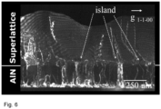
- the islands have a height of not less than 100 nm and not more than 1000 nm.
- the height is the maximum length of an island in a direction perpendicular to the surface of the wafer, i.e. in a direction perpendicular to a plane of the monocrystalline silicon substrate having a ⁇ 111 ⁇ orientation.
- the height refers to the height of the islands at the time of coalescence. If the height of the islands falls within the range of 100 to 1000 nm, the annihilation of dislocations is promoted and thermally induced stress is compensated. In the present invention, the height of the islands is also referred to as thickness of the islands.
- the one or more monocrystalline, doped GaN layers may contain a p-type dopant and/or an n-type dopant.
- the p-type dopant is preferably one or more element selected from the group consisting of Mg, Be, Zn and C.
- the n-type dopant is preferably one or more element selected from the group consisting of Si, Ge, Sn, O and C.
- the Si concentration in a Si-doped GaN layer is preferably not less than 1.0 ⁇ 10 15 cm -3 and not more than 5.0 ⁇ 10 19 cm -3 , more preferably not less than 1.0 ⁇ 10 15 cm -3 and not more than 1.0 ⁇ 10 18 cm -3 . If the Si-doped GaN layer is used as a drift layer, the Si concentration is preferably not less than 1.0 ⁇ 10 15 cm -3 and not more than 5.0 ⁇ 10 -6 cm -3 .
- a low temperature AlN nucleation layer is deposited by flowing a gas stream comprising an aluminum precursor and a nitrogen precursor over the substrate at a temperature of not less than 700 °C and not more than 900 °C, preferably not less than 750 °C and not more than 850 °C.
- the low temperature AlN nucleation layer is preferably a layer as defined in the first aspect of the present invention and has the purpose of providing nucleation sites for the growth of the high temperature AlN layer.
- step (vi) Al x Ga 1-x N with 0.7 ⁇ x ⁇ 1.0 and Al y Ga 1-y N with 0 ⁇ y ⁇ 0.5 is deposited alternately for 20 to 100 cycles by flowing a gas stream comprising an aluminum precursor, a gallium precursor and a nitrogen precursor, and optionally a carrier gas such as hydrogen, over the substrate at a temperature of not less than 1000°C and not more than 1100°C.
- a carrier gas such as hydrogen
- Al x Ga 1-x N with 0.80 ⁇ x ⁇ 1.00 and Al y Ga 1-y N with 0.05 ⁇ y ⁇ 0.40 is deposited.
- step (vi) islands and a super lattice structure is formed.
- the vertical growth rate i.e. the growth rate in a direction perpendicular to a plane of the monocrystalline silicon substrate with a ⁇ 111 ⁇ orientation
- the horizontal growth rate i.e. the growth rate along a plane of the monocrystalline silicon substrate with a ⁇ 111 ⁇ orientation.
- the dimensions, shape and density of the islands is controlled by the process conditions, in particular the temperature, pressure and the atomic ratio of group (v) to group (iii) elements in the gas phase, wherein only group (V) and group (III) elements from precursor compounds are taken into account.
- the process of island formation is also determined by the strain of the underlying layers. After the first cycles, preferably after not more than 20 cycles, the ratio of the vertical growth rate to the horizontal growth rate is decreased, so that the islands coalesce and continuous layers are deposited. During the transition from island growth to the deposition of continuous layers, new dislocations, in particular threading dislocations, can be generated at the coalescence boundaries.
- the alternation of the deposition in each cycle of step (vi) is achieved by changing the composition of the gas stream so that the atomic ratio of group (V) elements resulting from the nitrogen precursor to group (III) elements resulting from the aluminum precursor, and if present from the gallium precursor, in the gas stream is alternated between a first value of not more than 100 and a second value of not less than 200.
- the ratio of Al to Ga in the gas stream can be adjusted, in order to control the composition of the layers deposited in steps (v) and (vi). More preferably, the first value is not more than 50 and the second value is not less than 300. Most preferably, the first value is not less than 5 and not more than 50 and the second value is not less than 300 and not more than 500.
- the growth rate throughout steps (i) to (iv) is preferably in the range of 100 to 1500 nm/h.
- the growth rate is more preferably in the range of 100 to 300 nm/h.
- the growth rate of Al x Ga 1-x N is in the range of 100 to 500 nm/h and the growth rate of Al y Ga 1-y N is in the range of 700 to 1300 nm/h.
- the growth rate can be influenced by adjusting the temperature, the flow rate, the total pressure in the reaction chamber and the precursor concentration in the gas flow.
- the gas stream is preferably adjusted according to the desired composition of the doped GaN layer for each layer to be deposited.
Landscapes
- Crystals, And After-Treatments Of Crystals (AREA)
- Recrystallisation Techniques (AREA)
Priority Applications (3)
| Application Number | Priority Date | Filing Date | Title |
|---|---|---|---|
| EP23203112.0A EP4539100A1 (fr) | 2023-10-12 | 2023-10-12 | Plaquette semi-conductrice à structure multicouche et son procédé de fabrication |
| PCT/EP2024/056000 WO2025078038A1 (fr) | 2023-10-12 | 2024-03-07 | Tranche semi-conductrice ayant une structure multicouches et son procédé de production |
| TW113115148A TWI889303B (zh) | 2023-10-12 | 2024-04-23 | 具有多層結構的半導體晶圓及其製造方法 |
Applications Claiming Priority (1)
| Application Number | Priority Date | Filing Date | Title |
|---|---|---|---|
| EP23203112.0A EP4539100A1 (fr) | 2023-10-12 | 2023-10-12 | Plaquette semi-conductrice à structure multicouche et son procédé de fabrication |
Publications (1)
| Publication Number | Publication Date |
|---|---|
| EP4539100A1 true EP4539100A1 (fr) | 2025-04-16 |
Family
ID=88373688
Family Applications (1)
| Application Number | Title | Priority Date | Filing Date |
|---|---|---|---|
| EP23203112.0A Pending EP4539100A1 (fr) | 2023-10-12 | 2023-10-12 | Plaquette semi-conductrice à structure multicouche et son procédé de fabrication |
Country Status (3)
| Country | Link |
|---|---|
| EP (1) | EP4539100A1 (fr) |
| TW (1) | TWI889303B (fr) |
| WO (1) | WO2025078038A1 (fr) |
Citations (3)
| Publication number | Priority date | Publication date | Assignee | Title |
|---|---|---|---|---|
| WO2011102044A1 (fr) * | 2010-02-16 | 2011-08-25 | 日本碍子株式会社 | Substrat épitaxial et procédé de fabrication de celui-ci |
| JP2013069983A (ja) * | 2011-09-26 | 2013-04-18 | Sharp Corp | 窒化物半導体層を成長させるためのバッファ層構造を有する基板の製造方法 |
| EP2727133B1 (fr) | 2011-06-30 | 2020-05-20 | Soitec | Procédé de fabrication d'une couche épitaxiale épaisse de nitrure de gallium sur un substrat de silicium ou similaire et couche obtenue à l'aide dudit procédé |
Family Cites Families (10)
| Publication number | Priority date | Publication date | Assignee | Title |
|---|---|---|---|---|
| WO2017111869A1 (fr) * | 2015-12-24 | 2017-06-29 | Intel Corporation | Dichalcogénures de métaux de transition (tmdc) sur couches hétéroépitaxiales de nitrures du groupe iii |
| CN105591004B (zh) * | 2016-03-29 | 2020-07-10 | 苏州晶湛半导体有限公司 | 基于图形化Si衬底的LED外延片及其制备方法 |
| WO2018120363A1 (fr) * | 2016-12-31 | 2018-07-05 | 华南理工大学 | Dispositif hemt amélioré à base de gan basé sur un substrat en si et procédé de fabrication associé |
| CN111164733B (zh) * | 2017-07-20 | 2024-03-19 | 斯维甘公司 | 用于高电子迁移率晶体管的异质结构及其生产方法 |
| EP3451364B1 (fr) * | 2017-08-28 | 2020-02-26 | Siltronic AG | Plaquette hétéroepitaxiale et procédé de fabrication d'une plaquette hétéroepitaxiale |
| EP3486939B1 (fr) * | 2017-11-20 | 2020-04-01 | IMEC vzw | Procédé de formation d'une structure de semi-conducteurs pour un dispositif de canal de nitrure de gallium |
| CN108695385B (zh) * | 2018-07-17 | 2024-04-05 | 中山市华南理工大学现代产业技术研究院 | 一种基于Si衬底的GaN基射频器件外延结构及其制造方法 |
| CN114747018A (zh) * | 2019-12-03 | 2022-07-12 | 剑桥电子有限公司 | 具有改进的漏极接近区域的iii族氮化物晶体管 |
| CN112760611B (zh) * | 2020-12-22 | 2022-12-27 | 温州大学激光与光电智能制造研究院 | 一种提高mocvd外延薄膜质量的优化生长方法 |
| TWI818379B (zh) * | 2021-12-08 | 2023-10-11 | 財團法人工業技術研究院 | 高電子遷移率電晶體元件 |
-
2023
- 2023-10-12 EP EP23203112.0A patent/EP4539100A1/fr active Pending
-
2024
- 2024-03-07 WO PCT/EP2024/056000 patent/WO2025078038A1/fr active Pending
- 2024-04-23 TW TW113115148A patent/TWI889303B/zh active
Patent Citations (3)
| Publication number | Priority date | Publication date | Assignee | Title |
|---|---|---|---|---|
| WO2011102044A1 (fr) * | 2010-02-16 | 2011-08-25 | 日本碍子株式会社 | Substrat épitaxial et procédé de fabrication de celui-ci |
| EP2727133B1 (fr) | 2011-06-30 | 2020-05-20 | Soitec | Procédé de fabrication d'une couche épitaxiale épaisse de nitrure de gallium sur un substrat de silicium ou similaire et couche obtenue à l'aide dudit procédé |
| JP2013069983A (ja) * | 2011-09-26 | 2013-04-18 | Sharp Corp | 窒化物半導体層を成長させるためのバッファ層構造を有する基板の製造方法 |
Non-Patent Citations (5)
| Title |
|---|
| A. DADGAR ET AL., PHYS. STAT. SOL., vol. 0, no. 6, 2003 |
| A. E. ROMANOVJ. S. SPECK., APPL. PHYS. LETT., vol. 83, no. 13, 2003, pages 2569 - 2571 |
| B. DAUDIN, B. ET AL., PHYS. REV. B, vol. 56, no. 12, 1997, pages R7069 |
| M. IMURA ET AL., J. CRYST. GROWTH, vol. 300, no. 1, 2007, pages 136 - 140 |
| Y. ZHANG ET AL., J. PHYS. D: APPL. PHYS., vol. 51, 2018, pages 273001 |
Also Published As
| Publication number | Publication date |
|---|---|
| TW202517054A (zh) | 2025-04-16 |
| WO2025078038A1 (fr) | 2025-04-17 |
| TWI889303B (zh) | 2025-07-01 |
Similar Documents
| Publication | Publication Date | Title |
|---|---|---|
| JP5818853B2 (ja) | n型窒化アルミニウム単結晶基板を用いた縦型窒化物半導体デバイス | |
| EP1745165B1 (fr) | Procede de production de substrats ge virtuels pour integration iii-v sur si(001) | |
| CN108352306B (zh) | 半导体元件用外延基板、半导体元件和半导体元件用外延基板的制造方法 | |
| Bremser et al. | Growth, doping and characterization of AlxGa1− xN thin film alloys on 6H-SiC (0001) substrates | |
| US7323764B2 (en) | Buffer structure for modifying a silicon substrate | |
| US11476116B2 (en) | Manufacturing method of gallium oxide thin film for power semiconductor using dopant activation technology | |
| EP2819152A1 (fr) | Élément semi-conducteur et son procédé de fabrication | |
| GB2192198A (en) | Preparing compound semiconductor | |
| JP5179635B1 (ja) | 窒化物半導体層を成長させるためのバッファ層構造を有する基板の製造方法 | |
| TW201919238A (zh) | 用於高電子遷移率電晶體之異質結構及其製造方法 | |
| CN103367589A (zh) | 用于制造含Ga的第III族氮化物半导体的方法 | |
| US6339014B1 (en) | Method for growing nitride compound semiconductor | |
| CN110610849B (zh) | 一种InGaN半导体材料及其外延制备方法和应用 | |
| EP4539100A1 (fr) | Plaquette semi-conductrice à structure multicouche et son procédé de fabrication | |
| Davis et al. | Gas-source molecular beam epitaxy of III–V nitrides | |
| JP2011066333A (ja) | 電子デバイス用エピタキシャル基板およびその製造方法ならびにiii族窒化物電子デバイス用エピタキシャル基板 | |
| CN108511326A (zh) | 一种化合物半导体材料InGaN及其外延制备方法 | |
| CN110364420A (zh) | 一种插入InGaN/GaN超晶格结构改善非极性GaN材料质量的外延生长方法 | |
| KR101041659B1 (ko) | 산화아연 버퍼층을 이용한 질화갈륨 에피층 제조방법 | |
| JP4535935B2 (ja) | 窒化物半導体薄膜およびその製造方法 | |
| CN121218665B (zh) | 氮化镓异质外延结构及其制备方法 | |
| Bessolov et al. | Semipolar Wide-Band III–N-Layers on a Silicon Substrate: Orientation Controlling Epitaxy and the Properties of Structures | |
| US20250290226A1 (en) | Semiconductor structure and manufacturing method thereof | |
| RU2750295C1 (ru) | Способ изготовления гетероэпитаксиальных слоев III-N соединений на монокристаллическом кремнии со слоем 3C-SiC | |
| US20160020359A1 (en) | Nitride semiconductor crystal and method of fabricating the same |
Legal Events
| Date | Code | Title | Description |
|---|---|---|---|
| PUAI | Public reference made under article 153(3) epc to a published international application that has entered the european phase |
Free format text: ORIGINAL CODE: 0009012 |
|
| STAA | Information on the status of an ep patent application or granted ep patent |
Free format text: STATUS: THE APPLICATION HAS BEEN PUBLISHED |
|
| AK | Designated contracting states |
Kind code of ref document: A1 Designated state(s): AL AT BE BG CH CY CZ DE DK EE ES FI FR GB GR HR HU IE IS IT LI LT LU LV MC ME MK MT NL NO PL PT RO RS SE SI SK SM TR |
|
| STAA | Information on the status of an ep patent application or granted ep patent |
Free format text: STATUS: REQUEST FOR EXAMINATION WAS MADE |
|
| 17P | Request for examination filed |
Effective date: 20250505 |