EP4539251A1 - Dispositif électronique comprenant une antenne - Google Patents
Dispositif électronique comprenant une antenne Download PDFInfo
- Publication number
- EP4539251A1 EP4539251A1 EP23875269.5A EP23875269A EP4539251A1 EP 4539251 A1 EP4539251 A1 EP 4539251A1 EP 23875269 A EP23875269 A EP 23875269A EP 4539251 A1 EP4539251 A1 EP 4539251A1
- Authority
- EP
- European Patent Office
- Prior art keywords
- connection member
- electronic device
- circuit board
- sidewall
- antenna
- Prior art date
- Legal status (The legal status is an assumption and is not a legal conclusion. Google has not performed a legal analysis and makes no representation as to the accuracy of the status listed.)
- Pending
Links
Images


Classifications
-
- H—ELECTRICITY
- H01—ELECTRIC ELEMENTS
- H01Q—ANTENNAS, i.e. RADIO AERIALS
- H01Q9/00—Electrically-short antennas having dimensions not more than twice the operating wavelength and consisting of conductive active radiating elements
- H01Q9/04—Resonant antennas
- H01Q9/30—Resonant antennas with feed to end of elongated active element, e.g. unipole
- H01Q9/42—Resonant antennas with feed to end of elongated active element, e.g. unipole with folded element, the folded parts being spaced apart a small fraction of the operating wavelength
-
- H—ELECTRICITY
- H01—ELECTRIC ELEMENTS
- H01Q—ANTENNAS, i.e. RADIO AERIALS
- H01Q1/00—Details of, or arrangements associated with, antennas
- H01Q1/12—Supports; Mounting means
- H01Q1/22—Supports; Mounting means by structural association with other equipment or articles
- H01Q1/24—Supports; Mounting means by structural association with other equipment or articles with receiving set
- H01Q1/241—Supports; Mounting means by structural association with other equipment or articles with receiving set used in mobile communications, e.g. GSM
- H01Q1/242—Supports; Mounting means by structural association with other equipment or articles with receiving set used in mobile communications, e.g. GSM specially adapted for hand-held use
- H01Q1/243—Supports; Mounting means by structural association with other equipment or articles with receiving set used in mobile communications, e.g. GSM specially adapted for hand-held use with built-in antennas
-
- H—ELECTRICITY
- H01—ELECTRIC ELEMENTS
- H01Q—ANTENNAS, i.e. RADIO AERIALS
- H01Q1/00—Details of, or arrangements associated with, antennas
- H01Q1/12—Supports; Mounting means
- H01Q1/22—Supports; Mounting means by structural association with other equipment or articles
-
- H—ELECTRICITY
- H01—ELECTRIC ELEMENTS
- H01Q—ANTENNAS, i.e. RADIO AERIALS
- H01Q1/00—Details of, or arrangements associated with, antennas
- H01Q1/48—Earthing means; Earth screens; Counterpoises
-
- H—ELECTRICITY
- H01—ELECTRIC ELEMENTS
- H01Q—ANTENNAS, i.e. RADIO AERIALS
- H01Q21/00—Antenna arrays or systems
- H01Q21/0006—Particular feeding systems
-
- H—ELECTRICITY
- H01—ELECTRIC ELEMENTS
- H01Q—ANTENNAS, i.e. RADIO AERIALS
- H01Q21/00—Antenna arrays or systems
- H01Q21/28—Combinations of substantially independent non-interacting antenna units or systems
-
- H—ELECTRICITY
- H01—ELECTRIC ELEMENTS
- H01Q—ANTENNAS, i.e. RADIO AERIALS
- H01Q21/00—Antenna arrays or systems
- H01Q21/30—Combinations of separate antenna units operating in different wavebands and connected to a common feeder system
-
- H—ELECTRICITY
- H04—ELECTRIC COMMUNICATION TECHNIQUE
- H04M—TELEPHONIC COMMUNICATION
- H04M1/00—Substation equipment, e.g. for use by subscribers
- H04M1/02—Constructional features of telephone sets
-
- H—ELECTRICITY
- H04—ELECTRIC COMMUNICATION TECHNIQUE
- H04M—TELEPHONIC COMMUNICATION
- H04M1/00—Substation equipment, e.g. for use by subscribers
- H04M1/02—Constructional features of telephone sets
- H04M1/23—Construction or mounting of dials or of equivalent devices; Means for facilitating the use thereof
Definitions
- Embodiments of the disclosure relate to an antenna assembly and an electronic device including the same.
- the term "electronic device” may mean a device performing a particular function according to its equipped program, such as a home appliance, an electronic scheduler, a portable multimedia player, a mobile communication terminal, a tablet PC, a video/sound device, a desktop PC or laptop computer, a navigation for automobile, etc.
- the electronic devices may output stored information as voices or images.
- An electronic device may include an antenna device that provides wireless communication in various frequency bands. As such an antenna device meets a high gain and wide beam coverage, communication performance of the electronic device may be provided with stable quality under a commercialized wireless communication network environment.
- communication such as mobile communication (e.g., 2G/3G/4G/UMTS/LTE), Bluetooth, Wi-Fi, NFC, GPS, and UWB in low/medium/high frequency bands of several GHz or less supporting multiple bands, as well as millimeter wave communication having a frequency band of several tens of GHz or more (e.g., a high-band frequency of 28 GHz or more), has been used to meet demand for soaring data traffic.
- An electronic device may include a plate, a side frame, a printed circuit board, a key assembly, and/or at least one antenna module.
- the side frame may disposed at an edge of the plate and include a first sidewall.
- the first sidewall may extend in at least one axial direction and including at least one conductive portion.
- the printed circuit board may be disposed on one surface of the plate and may include at least one ground area.
- the key assembly may be disposed on a portion of the side frame and may include a first flexible circuit board connected to the printed circuit board.
- the antenna module may include the at least one conductive portion and a plurality of connection members.
- the plurality of connection members may include a first connection member disposed inside the first sidewall, a second connection member disposed inside the first sidewall to be spaced apart from the first connection member and a third connection member disposed between the first connection member and the second connection member.
- Each of the first connection member and the second connection may be electrically connected to at least one conductive portion and the first flexible circuit board.
- the third connection member may be electrically connected to at least one the conductive portion and the ground area.
- the electronic device 101 in the network environment 100 may communicate with an electronic device 102 via a first network 198 (e.g., a short-range wireless communication network), or an electronic device 104 or a server 108 via a second network 199 (e.g., a long-range wireless communication network).
- a first network 198 e.g., a short-range wireless communication network
- an electronic device 104 or a server 108 via a second network 199 (e.g., a long-range wireless communication network).
- the electronic device 101 may communicate with the electronic device 104 via the server 108.
- the memory 130 may store various data used by at least one component (e.g., the processor 120 or the sensor module 176) of the electronic device 101.
- the various data may include, for example, software (e.g., the program 140) and input data or output data for a command related thereto.
- the memory 130 may include the volatile memory 132 or the non-volatile memory 134.
- the sensor module 176 may detect an operational state (e.g., power or temperature) of the electronic device 101 or an environmental state (e.g., a state of a user) external to the electronic device 101, and then generate an electrical signal or data value corresponding to the detected state.
- the sensor module 176 may include, for example, a gesture sensor, a gyro sensor, an atmospheric pressure sensor, a magnetic sensor, an accelerometer, a grip sensor, a proximity sensor, a color sensor, an infrared (IR) sensor, a biometric sensor, a temperature sensor, a humidity sensor, or an illuminance sensor.
- the interface 177 may support one or more specified protocols to be used for the electronic device 101 to be coupled with the external electronic device (e.g., the electronic device 102) directly (e.g., wiredly) or wirelessly.
- the interface 177 may include, for example, a high definition multimedia interface (HDMI), a universal serial bus (USB) interface, a secure digital (SD) card interface, or an audio interface.
- HDMI high definition multimedia interface
- USB universal serial bus
- SD secure digital
- the camera module 180 may capture a still image or moving images.
- the camera module 180 may include one or more lenses, image sensors, image signal processors, or flashes.
- the wireless communication module 192 may support a peak data rate (e.g., 20Gbps or more) for implementing eMBB, loss coverage (e.g., 164dB or less) for implementing mMTC, or U-plane latency (e.g., 0.5ms or less for each of downlink (DL) and uplink (UL), or a round trip of 1ms or less) for implementing URLLC.
- a peak data rate e.g., 20Gbps or more
- loss coverage e.g., 164dB or less
- U-plane latency e.g., 0.5ms or less for each of downlink (DL) and uplink (UL), or a round trip of 1ms or less
- the signal or the power may then be transmitted or received between the communication module 190 and the external electronic device via the selected at least one antenna.
- other parts e.g., radio frequency integrated circuit (RFIC)
- RFIC radio frequency integrated circuit
- the one or more external electronic devices receiving the request may perform the at least part of the function or the service requested, or an additional function or an additional service related to the request, and transfer an outcome of the performing to the electronic device 101.
- the electronic device 101 may provide the outcome, with or without further processing of the outcome, as at least part of a reply to the request.
- a cloud computing, distributed computing, mobile edge computing (MEC), or client-server computing technology may be used, for example.
- the electronic device 101 may provide ultra low-latency services using, e.g., distributed computing or mobile edge computing.
- the external electronic device 104 may include an internet-of-things (IoT) device.
- the server 108 may be an intelligent server using machine learning and/or a neural network.
- the front plate 202 may include two first edge areas 210D, which seamlessly and bendingly extend from the first surface 210A to the rear cover 211, on both the long edges of the front plate 202.
- the rear cover 211 may include two second edge areas 210E, which seamlessly and bendingly extend from the rear surface 210B to the front plate 202, on both the long edges.
- the front plate 202 (or the rear cover 211) may include only one of the first edge areas 210D (or the second edge areas 210E).
- the first edge areas 210D or the second edge areas 210E may partially be excluded.
- the display 201 may be visually revealed through, e.g., a majority portion of the front plate 202. In an embodiment, at least a portion of the display 201 may be visually exposed through the front plate 202 forming the front surface 210A and the first edge areas 210D. In an embodiment, the edge of the display 201 may be formed to be substantially the same in shape as an adjacent outer edge of the front plate 202. In an embodiment, the interval between the outer edge of the display 201 and the outer edge of the front plate 202 may remain substantially even to give a larger area of exposure for the display 201.
- a recess or opening may be formed in a portion of the screen display area (e.g., the front surface 210A or the first edge area 210D) of the display 201, and at least one or more of the audio module 214, sensor module, light emitting device, and camera module 205 may be aligned with the recess or opening.
- at least one or more of the audio module 214, sensor module, camera module 205, fingerprint sensor, and light emitting device may be included on the rear surface of the screen display area of the display 201.
- the display 201 may be disposed to be coupled with, or adjacent to, a touch detecting circuit, a pressure sensor capable of measuring the strength (pressure) of touches, and/or a digitizer for detecting a magnetic field-type stylus pen.
- a touch detecting circuit capable of measuring the strength (pressure) of touches
- a digitizer for detecting a magnetic field-type stylus pen.
- at least part of the key input device 217 may be disposed in the first edge areas 210D and/or the second edge areas 210E.
- the electronic device 101 may include a plurality of camera modules (e.g., a dual camera or triple camera) having different attributes (e.g., angle of view) or functions.
- a plurality of camera modules 205 and 212 including lenses having different angles of view may be configured, and the electronic device 101 may control to change the angle of view of the camera modules 205 and 212 performed by the electronic device 101 based on the user's selection.
- At least one of the plurality of camera modules 205 and 212 may form, for example, a wide-angle camera and at least another of the plurality of camera modules may form a telephoto camera.
- the plurality of camera modules 205 and 212 may be a front camera and at least another of the plurality of camera modules may be a rear camera. Further, the plurality of camera modules 205 and 212 may include at least one of a wide-angle camera, a telephoto camera, and an infrared (IR) camera (e.g., a time of flight (TOF) camera, a structured light camera).
- IR infrared
- TOF time of flight
- the IR camera may be operated as at least a portion of the sensor module.
- the TOF camera may be operated as at least a portion of a sensor module for detecting the distance to the subject.
- the connector holes 208 and 209 may include, e.g., a first connector hole 208 for accommodating a connector (e.g., a universal serial bus (USB) connector) for transmitting or receiving power and/or data to/from an external electronic device and/or a second connector hole (e.g., an earphone jack) 209 for accommodating a connector for transmitting or receiving audio signals to/from the external electronic device.
- a connector e.g., a universal serial bus (USB) connector
- USB universal serial bus
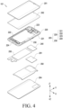
- FIG. 4 is an exploded perspective view illustrating an electronic device according to an embodiment of the disclosure.
- an electronic device 101 may include a supporting bracket 220 and 230, a front plate 202 (e.g., the front plate 202 of FIG. 2 ), a display module 201 (e.g., the display 201 of FIG. 2 ), a printed circuit board 240 (e.g., a PCB, flexible PCB (FPCB), or rigid flexible PCB (RFPCB)), a battery 250 (e.g., the battery 189 of FIG. 1 ), a second supporting member 291 (e.g., a rear structure), an antenna 292 (e.g., the antenna module 197 of FIG.
- a supporting bracket 220 and 230 may include a supporting bracket 220 and 230, a front plate 202 (e.g., the front plate 202 of FIG. 2 ), a display module 201 (e.g., the display 201 of FIG. 2 ), a printed circuit board 240 (e.g., a PCB, flexible PCB (FPCB), or rigid flexible PCB (
- a processor, a memory, and/or an interface may be mounted on the printed circuit board 240.
- the processor may include one or more of, e.g., a central processing unit, an application processor, a graphic processing device, an image signal processing, a sensor hub processor, or a communication processor.
- the printed circuit board 240 may include a flexible printed circuit board type radio frequency cable (FRC).
- FRC radio frequency cable
- the printed circuit board 240 may be disposed on at least a portion of the plate 230 and may be electrically connected with an antenna 292 (e.g., the antenna module 197 of FIG. 1 ) and a communication module (e.g., the communication module 190 of FIG. 1 ).
- the electronic device 101 may include a housing 203, a printed circuit board 240, a camera structure 260, a key assembly 270, and/or an antenna assembly 280.
- the side frame 220 forms the right frame (e.g., X-direction frame), the left frame (e.g., - X-direction frame), and a second sidewall (e.g., the second sidewall 222 of FIG. 4 ).
- the side frame 220 may include a pair of upper and lower sidewalls (e.g., Y-direction sidewalls) that connect the first sidewall 221 and the second sidewall and face each other.
- the side frame 220 may include a third sidewall 223 (e.g., the third sidewall 223 of FIG.
- the plate 230 may include an injection-molded area 230a formed in an area (e.g., an edge) contacting the side frame 220.
- the injection-molded area 230a may include a non-conductive material.
- a portion of the injection-molded material of the plate 230 may be disposed in the slit area 2211 of the side frame 220 to be described below. For example, referring to FIG.
- the surface of the injection-molded product disposed in the slit area 2211, together with the surface of the first sidewall 221, may form a portion of the exterior of the electronic device 101.
- at least a portion of the injection-molded area 230a may be referred to as a component included in the side frame 220.
- the camera structure 260 may include a plurality of camera devices. According to an embodiment, at least some of the plurality of camera devices may correspond to rear cameras exposed through the rear plate (e.g., the rear plate 204 of FIG. 4 ) of the electronic device 101. According to an embodiment, the camera structure 260 may include a first camera device 261, a second camera device 262, and/or a third camera device 263.
- the second camera device 262 may be disposed in the first seating area 236a, and the third camera device 263 may be disposed in the second seating area 236b.
- a first partition wall 236c may be positioned between the second camera device 262 and the third camera device 263.
- the camera structure 260 may be electrically connected to the printed circuit board 240, and for example, the camera structure 260 may not be provided with another additional circuit board.
- the electronic device 101 may establish a direct (e.g., wired) communication channel or a wireless communication channel with the external electronic device 101 (e.g., the electronic device 102, the electronic device 104, or the server 108 of FIG. 1 ) and may support communication through the established communication channel and may exchange signals with each other.
- a direct (e.g., wired) communication channel or a wireless communication channel with the external electronic device 101 (e.g., the electronic device 102, the electronic device 104, or the server 108 of FIG. 1 ) and may support communication through the established communication channel and may exchange signals with each other.
- the battery 250 may be electrically connected to the printed circuit board 240 by the second flexible circuit board 251.
- the second flexible circuit board 251 may be disposed between the battery 250 and the camera structure 260 (e.g., the third camera).
- the second flexible circuit board 251 may include two surfaces facing each other, and a plurality of signal lines may be disposed between the two surfaces.
- the key assembly 270 may include at least one key member 271, a first flexible circuit board 272, at least one shaft member 273, a key waterproof member 274, and/or a key bracket 275, a key supporting member 276, and/or a key circuit board 278.
- the following description of the components of the key assembly 270 is merely an example, and some components (e.g., the key member 271 and the shaft member 273) of the key assembly 270 may be changed or omitted depending on the type and function of the key assembly 270.
- the second board portion 272b may connect the board assembly (e.g., the first board portion 272a) and the printed circuit board 240, and may be disposed so as not to overlap other electrical components in the electronic device 101. Referring to FIG. 6 , in an embodiment, at least a portion of the second board portion 272b may be disposed between the third camera and the battery 250. For example, the second board portion 272b may be disposed to extend from the first board portion 272a to the printed circuit board 240 across between the second camera and the third camera.
- the first flexible circuit board 272 may be fixed such that one surface (e.g., a surface in the -Y direction) of the first flexible circuit board 272 faces a surface (e.g., a surface in the +Y direction) of the second partition wall 236d that faces the first partition wall 236c.
- the thickness of the first flexible circuit board 272 may cross (e.g., be orthogonal to) one surface of the second flexible circuit board 251.
- the thickness of the first flexible circuit board 272 may not overlap one surface of the second flexible circuit board 251.
- the thickness of the second flexible circuit board 251 may refer to the Z-axis direction dimension of FIGS. 7 to 9 with respect to a portion parallel to the second partition wall 236d.
- the width of the second board portion 272b described above may refer to the Z-axis direction dimension of FIGS. 7 to 9 with respect to a portion of the second board portion 272b disposed on the second partition wall 236d.
- the shaft member 273 may be disposed on the first board portion 272a to protrude toward the key member 271.
- the shaft member 273 may be configured to receive an external input (e.g., a touch or a pressing force) such as a click applied to the key member 271.
- the key member 271 may include an elastically deformable material.
- the shaft member 273 may be deformed in the pressing direction (e.g., the -X direction).
- the shaft member 273 may be restored to its original form to move the key member 271 in a direction (e.g., the +X direction) opposite to the pressing direction, and the key member 271 may be returned to its original position.
- a direction e.g., the +X direction
- the at least one shaft member 273 may overlap the one key member 271, e.g., in one axis (e.g., the width direction or the X axis direction of the electronic device 101).
- the first shaft member 273a and the second shaft member 273b may overlap and be connected to different areas of the first key member 271a.
- the first shaft member 273a may be activated when a portion of the first key member 271a overlapping the first shaft member 273a is pressed
- the second shaft member 273b may be activated when another partial area of the first key member 271a overlapping the second shaft member 273b is pressed.
- the third shaft member 273c may be connected to the second key member 271b, and when the second key member 271b is pressed, the third shaft member 273c may be activated.
- the key waterproof member 274 may be disposed on one surface (e.g., a surface in the +X direction) facing the key member 271 of the first board portion 272a.
- the key waterproof member 274 may be opened in areas overlapping the key shaft member 273.
- the key shaft member 273 may be disposed to protrude toward the key member 271 through the opening of the key waterproof member 274.
- the key bracket 275 may be disposed on another surface (e.g., the surface in the -X direction) of the first board portion 272a that faces the key waterproof member 274.
- the key bracket 275 may support and/or protect the first board portion 272a.
- some components e.g., the key waterproof member 274 and/or the key bracket 275 may be omitted.
- the key supporting member 276 may be disposed farther from the first sidewall 221 than other components of the key assembly 270.
- the key member 271 may be disposed between the printed circuit board 240 or the key supporting member 276 and the camera structure 260.
- the key supporting member 276 may be formed to be elastically deformable.
- the key supporting member 276 may also be displaced and/or elastically deformed in the pressing direction.
- the key supporting member 276 may return to its original form and move and/or deform the key waterproof member 274 and/or the key bracket 275, including the first flexible circuit board 272 disposed on one side (e.g., the +X direction), to its original position in a direction (e.g., the +X direction) opposite to the pressing direction.
- the shape and/or position of the key supporting member 276 may be changed or omitted.
- various communication methods such as 2/3/4G communication, Bluetooth, Wi-Fi, and/or ultra-wide band (UWB) as well as short-range communication such as near field communication (NFC), magnetic secure transmission (MST), and wireless charging, may be performed by utilizing the conductive portion of the side frame 220 as an antenna radiator.
- 2/3/4G communication Bluetooth, Wi-Fi, and/or ultra-wide band (UWB)
- short-range communication such as near field communication (NFC), magnetic secure transmission (MST), and wireless charging
- NFC near field communication
- MST magnetic secure transmission
- wireless charging may be performed by utilizing the conductive portion of the side frame 220 as an antenna radiator.
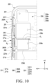
- the antenna assembly 280 may be disposed along a portion of the first sidewall 221.
- the antenna assembly 280 may include at least one conductive portion of the first sidewall 221, a plurality of connection members 281, 282, and 283, and a feeding signal line disposed on the first flexible circuit board 272.
- the conductive portion may be electrically connected to the first connection member 281 and/or the second connection member 283 connected to the feeding signal line to function as an antenna radiator.
- the antenna assembly 280 may include a first connection member 281, a second connection member 283, and/or a third connection member 282 disposed between the first connection member 281 and the second connection member 283, which are spaced apart from each other along the first sidewall 221.
- Each of the connection members 281, 282, and 283 may be electrically connected to a conductive portion of the first sidewall 221.
- the first connection member 281 and/or the second connection member 283 may be connected to a feeding signal line disposed on the first flexible circuit board 272.
- the third connection member 282 may be electrically connected to a ground area disposed on the printed circuit board 240.
- connection members 281, 282, and 283 may be electrically connected to conductive portions, respectively, disposed in different areas on the first sidewall 221.
- the connection members 281, 282, and 283 may include a conductive material such as metal, and may be, e.g., a clip member (e.g., C-clip).
- FIG. 10 is a view illustrating an antenna assembly of an electronic device according to an embodiment of the disclosure.
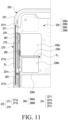
- FIG. 11 is a view illustrating an antenna assembly of an electronic device according to an embodiment of the disclosure.
- the first sidewall 221 may further include at least one extension member 221a, 221b, and 221c protruding toward the first board portion 272a (e.g., in the -X direction).
- the extension member may include a conductive material (e.g., metal).
- at least some of the extension members (e.g., the extension members of FIGS. 10 and 11 ) may be electrically connected to the connection members 281, 282, and 283 receiving the feeding signal among the connection members 281, 282, and 283 of the antenna assembly 280.
- connection members 221a, 221b, and 221c may be electrically connected to connection members (e.g., the first connection member 281 and the second connection member 283) grounded to the printed circuit board 240 among the connection members 281, 282, and 283 of the antenna assembly 280.
- the antenna assembly 280 may include a first antenna module 280A and a second antenna module 280B.
- the first connection member 281 and the second connection member 283 may correspond to feeding members respectively connected to feeding signal lines of the first flexible circuit board 272.
- the third connection member 282 may be electrically connected to a ground area of the printed circuit board 240.
- a plurality (e.g., three) of extension members 221a, 221b, and 221c may be provided.
- the plurality of extension members 221a, 221b, and 221c may include a first extension member 221a electrically connected to the first connection member 281, a second extension member 221b electrically connected to the second connection member 283, and/or a third extension member 221c electrically connected to the third connection member 282.
- the first antenna module 280A may include a second connection member 283 that is a feeding member, and a conductive portion of the first sidewall 221 electrically connected to the second connection member 283.
- the conductive portion functioning as the radiator of the second antenna module 280B may be referred to as a second conductive portion.
- the second conductive portion of the second antenna module 280B may be formed in different areas separated with respect to the first conductive portion of the first antenna module 280A and the third connection member 282.
- the second antenna module 280B may include a second antenna pattern P B formed on the second conductive portion.
- the second antenna module 280B may radiate a frequency signal in a second designated range through an electrical path of the second antenna pattern P B .
- the second antenna module 280B may transmit and/or receive the frequency signal in the second designated range to/from the external electronic device 101 (e.g., the electronic device 102 or the electronic device 104 of FIG. 1 ).
- the first designated range of the first antenna module 280A and the second designated range of the second antenna module 280B may be different from each other, or may at least partially overlap each other.
- the first antenna module 280A may operate as a slot antenna.
- the length of the first antenna pattern P A may be about 1/2 of the wavelength ⁇ of the second antenna module 280B.
- the third connection member 282 which is a ground member, is disposed between the first antenna module 280A and the second antenna module 280B, and the first antenna module 280A and the second antenna module 280B are grounded differently from each other, thereby suppressing interference between the two antenna modules 280A and 280B and enhancing isolation.
- the antenna assembly 280 may function as a single antenna module.
- the antenna assembly 280 may include a third extension member 221c which is a single member.
- the third extension member 221c may be electrically connected to the third connection member 282.
- the antenna assembly 280 may include a third connection member 282, which is a feeding member, and a conductive portion of a third sidewall electrically connected to the third connection member 282.
- the second connection member 283 may correspond to a feeding member connected to a feeding signal line of the first flexible circuit board 272.
- the third connection member 282 may be electrically connected to a ground area of the printed circuit board 240.
- the first connection member 281 may be connected to the third connection member 282 at one point (e.g., CCP) and may be grounded to the printed circuit board 240 through the third connection member 282.
- the antenna assembly 280 may electrically connect the conductive portion to the ground area through the plurality of connection members 281 and 283, thereby providing stable antenna performance as compared to the case of grounding through one connection member (e.g., the third connection member 282).
- the antenna assembly 280 may include a third antenna pattern P C formed on the conductive portion.
- the antenna assembly 280 may radiate a frequency signal in a third designated range by an electrical path of the third antenna pattern P C .
- the third designated range may differ from, or may at least partially overlap, the first designated range and/or the second designated range of the embodiment of FIG. 10 .
- the antenna assembly 280 may transmit and/or receive a frequency signal in the third designated range to/from the external electronic device 101 (e.g., the electronic device 102 or the electronic device 104 of FIG. 1 ).
- the third antenna pattern P C may be formed on the first sidewall 221 between a partial area adjacent to the slit area 2211 and a partial area positioned lower than the second connection member 283 (e.g., in the -Y direction).
- the antenna assembly 280 of FIG. 11 may operate as a slit antenna.
- FIG. 12 is a graph illustrating radiation performance of an antenna assembly of an electronic device according to an embodiment of the disclosure.
- FIG. 13 is a graph illustrating radiation performance of an antenna assembly 280 of an electronic device 101 according to an embodiment of the disclosure.
- the x-axis of FIGS. 12 and 13 may represent a frequency band (frequency/GHz), and the y-axis may represent the performance of the antenna (the strength dB of the received signal).
- Graph S0 of FIGS. 12 and 13 may represent antenna performance when the third connection member 282, which is a ground member, is not disposed between the first antenna module 280A and the second antenna module 280B.
- Graphs S1 and S2 of FIGS. 12 and 13 respectively, may represent when the third connection member 282 is not electrically connected to a ground area corresponding to the main ground of the printed circuit board 240 and when the third connection member 282 is connected to the ground area in a case where the third connection member 282, which is a ground member, is disposed between the first antenna module 280A and the second antenna module 280B.
- graph S2 may represent the performance of the antenna assembly 280 according to an embodiment described above with reference to FIGS. 4 to 10 . Referring to FIGS.
- An electronic device may include a housing including a conductive material such as metal.
- the housing may include a sidewall (or a side frame) on which a side key assembly is disposed.
- a portion hereinafter, referred to as a "side radiator" of the sidewall adjacent to the side key assembly may be utilized as an antenna radiator.
- LDS laser direct structuring
- the feeding signal line of the side radiator may be provided to extend to the main circuit board.
- the feeding signal line includes an analog signal line, electromagnetic interference may occur when the feeding signal line is disposed to overlap another electrical component (e.g., a flexible circuit board of a side key assembly) including the digital signal line.
- An antenna assembly is to use a portion of a conductive sidewall as an antenna radiator.
- an antenna assembly that suppresses electromagnetic interference by placing a feeding signal line of an antenna radiator extending to the main circuit board not to overlap another electrical component including a digital, signal line when the other electrical component is disposed between it and the main circuit board and an electronic device including the antenna assembly.
- an antenna structure may be formed by utilizing an existing electrical component, e.g., in a method of including a signal line for feeding an antenna radiator of a sidewall in a flexible circuit board of a side key assembly.
- An electronic device 101 may include a plate 230, a side frame 220, a printed circuit board 240, a key assembly 270, and/or at least one antenna module 280; 280A; 280B.
- the side frame may disposed at an edge of the plate and include a first sidewall.
- the first sidewall may extend in at least one axial direction and including at least one conductive portion.
- the printed circuit board may be disposed on one surface of the plate and may include at least one ground area.
- the key assembly may be disposed on a portion of the side frame and may include a first flexible circuit board connected to the printed circuit board.
- the antenna module may include the at least one conductive portion and a plurality of connection members.
- the plurality of connection members may include a first connection member 281 disposed inside the first sidewall, a second connection member 283 disposed inside the first sidewall to be spaced apart from the first connection member and a third connection member 282 disposed between the first connection member and the second connection member.
- Each of the first connection member and the second connection may be electrically connected to at least one conductive portion and the first flexible circuit board.
- the third connection member may be electrically connected to at least one the conductive portion and the ground area.
- the antenna module may include at least one first signal line accommodated in the first flexible circuit board and configured to transmit a feeding signal.
- the at least one first signal line may be electrically connected to at least one of the first connection member or the second connection member.
- the first flexible circuit board may include at least one second signal line configured to transmit a digital signal and electrically connecting the key assembly and the printed circuit board.
- the electrical component may include a battery 250 and at least one second flexible circuit board 251 configured to connect the battery and the printed circuit board.
- the antenna module may include a first antenna module 280A electrically connected to the first connection member and/or a second antenna module 280B spaced apart from the first antenna module along the first sidewall with the third connection member interposed therebetween and electrically connected to the second connection member.
- the first antenna module may include the first connection member; and a first conductive portion of the at least one conductive portion, the first conductive portion configured to receive a feeding signal from the first connection member.
- the second antenna module may include the second connection member; and a second conductive portion of the at least one conductive portion, the second conductive portion configured to receive a feeding signal from the second connection member.
- the first conductive portion may be formed on a portion of the first sidewall.
- the second conductive portion may be formed on another portion of the first sidewall spaced apart from the first conductive portion with the third connection member interposed therebetween.
- the first antenna module may be grounded to the third connection member through an electrical path formed between the first connection member and the third connection member.
- the second antenna module may be grounded to the third connection member through an electrical path formed between the second connection member and the third connection member.
- the first sidewall may include a slit area 2211 formed through an area of the first sidewall adjacent to the first connection member.
- the first connection member is disposed between the slit area and the third connection member.
- the first antenna module may be a slit antenna.
- the second antenna module may be a slot antenna.
- the first sidewall may include a plurality of extension members 221a, 221b, and 221c protruding toward the first connection member, the second connection member, and the third connection member.
- the extension members may be electrically connected to the first connection member, the second connection member, and the second connection member.
- the first flexible circuit board may include a first board portion 272a where at least some of the first connection member, the second connection member, or the third connection member are disposed on one surface of the first board portion facing the first sidewall.
- the first flexible circuit board may include a second board portion 272b connecting the first board portion and the printed circuit board.
- An electronic device may include a plate 230, a side frame 220, a printed circuit board 240, a key assembly 270, and/or an antenna assembly 280.
- the side frame may include a first sidewall 221 disposed at an edge of the plate, extending in at least one axial direction, and including at least one conductive portion.
- the printed circuit board may be disposed on one surface of the plate and may include at least one ground area.
- the key assembly may be disposed on a portion of the side frame and may include a first flexible circuit board 272 connected to the printed circuit board.
- the antenna assembly may at least one first signal line accommodated in the first flexible circuit board and configured to transmit a feeding signal.
- the at least one first signal line may be electrically connected to at least one of the first connection member or the second connection member.
- the first connection member may be connected to the second connection member at one point through a first electrical path.
- the second connection member may be connected to the ground area through a second electrical path from the one point.
- the electronic device may be one of various types of electronic devices.
- the electronic devices may include, for example, a portable communication device (e.g., a smartphone), a computer device, a portable multimedia device, a portable medical device, a camera, a wearable device, or a home appliance.
- a portable communication device e.g., a smartphone
- a computer device e.g., a laptop, a desktop, a tablet, or a portable multimedia device
- a portable medical device e.g., a portable medical device
- camera e.g., a camera
- a wearable device e.g., a portable medical device
- each of such phrases as “A or B,” “at least one of A and B,” “at least one of A or B,” “A, B, or C,” “at least one of A, B, and C,” and “at least one of A, B, or C,” may include all possible combinations of the items enumerated together in a corresponding one of the phrases.
- such terms as “1st” and “2nd,” or “first” and “second” may be used to simply distinguish a corresponding component from another, and does not limit the components in other aspect (e.g., importance or order).
- an element e.g., a first element
- the element may be coupled with the other element directly (e.g., wiredly), wirelessly, or via a third element.
- module may include a unit implemented in hardware, software, or firmware, and may interchangeably be used with other terms, for example, “logic,” “logic block,” “part,” or “circuitry”.
- a module may be a single integral component, or a minimum unit or part thereof, adapted to perform one or more functions.
- the module may be implemented in a form of an application-specific integrated circuit (ASIC).
- ASIC application-specific integrated circuit
- a method according to an embodiment of the disclosure may be included and provided in a computer program product.
- the computer program products may be traded as commodities between sellers and buyers.
- the computer program product may be distributed in the form of a machine-readable storage medium (e.g., compact disc read only memory (CD-ROM)), or be distributed (e.g., downloaded or uploaded) online via an application store (e.g., Play Store TM ), or between two user devices (e.g., smartphones) directly. If distributed online, at least part of the computer program product may be temporarily generated or at least temporarily stored in the machine-readable storage medium, such as memory of the manufacturer's server, a server of the application store, or a relay server.
- CD-ROM compact disc read only memory
- an application store e.g., Play Store TM
- two user devices e.g., smartphones
- each component e.g., a module or a program of the above-described components may include a single entity or multiple entities. Some of the plurality of entities may be separately disposed in different components. According to an embodiment, one or more of the above-described components may be omitted, or one or more other components may be added. Alternatively or Further, a plurality of components (e.g., modules or programs) may be integrated into a single component. In such a case, according to various embodiments, the integrated component may still perform one or more functions of each of the plurality of components in the same or similar manner as they are performed by a corresponding one of the plurality of components before the integration.
Landscapes
- Engineering & Computer Science (AREA)
- Signal Processing (AREA)
- Computer Networks & Wireless Communication (AREA)
- Telephone Set Structure (AREA)
Applications Claiming Priority (3)
| Application Number | Priority Date | Filing Date | Title |
|---|---|---|---|
| KR20220127899 | 2022-10-06 | ||
| KR1020220146152A KR20240048438A (ko) | 2022-10-06 | 2022-11-04 | 안테나를 포함하는 전자 장치 |
| PCT/KR2023/015437 WO2024076208A1 (fr) | 2022-10-06 | 2023-10-06 | Dispositif électronique comprenant une antenne |
Publications (2)
| Publication Number | Publication Date |
|---|---|
| EP4539251A1 true EP4539251A1 (fr) | 2025-04-16 |
| EP4539251A4 EP4539251A4 (fr) | 2025-09-24 |
Family
ID=90573639
Family Applications (1)
| Application Number | Title | Priority Date | Filing Date |
|---|---|---|---|
| EP23875269.5A Pending EP4539251A4 (fr) | 2022-10-06 | 2023-10-06 | Dispositif électronique comprenant une antenne |
Country Status (3)
| Country | Link |
|---|---|
| US (1) | US20240120643A1 (fr) |
| EP (1) | EP4539251A4 (fr) |
| CN (1) | CN119999011A (fr) |
Family Cites Families (4)
| Publication number | Priority date | Publication date | Assignee | Title |
|---|---|---|---|---|
| TWI479809B (zh) * | 2013-02-04 | 2015-04-01 | Wistron Corp | 行動通訊裝置 |
| US10727569B2 (en) * | 2016-12-21 | 2020-07-28 | Htc Corporation | Mobile device and manufacturing method thereof |
| CN110336113B (zh) * | 2019-05-09 | 2021-07-20 | 天通凯美微电子有限公司 | 一种可重构天线与显示屏组件集成的电子设备 |
| KR20220046990A (ko) * | 2020-10-08 | 2022-04-15 | 삼성전자주식회사 | 안테나를 포함하는 전자 장치 |
-
2023
- 2023-10-06 CN CN202380070731.0A patent/CN119999011A/zh active Pending
- 2023-10-06 EP EP23875269.5A patent/EP4539251A4/fr active Pending
- 2023-10-06 US US18/377,628 patent/US20240120643A1/en active Pending
Also Published As
| Publication number | Publication date |
|---|---|
| US20240120643A1 (en) | 2024-04-11 |
| CN119999011A (zh) | 2025-05-13 |
| EP4539251A4 (fr) | 2025-09-24 |
Similar Documents
| Publication | Publication Date | Title |
|---|---|---|
| US11502413B2 (en) | Electronic device including antenna that radiates waves by a non-conducting portion | |
| EP4224629B1 (fr) | Appareil électronique comprenant une antenne et une carte de circuit imprimé | |
| US12418098B2 (en) | Antenna and electronic device including the same | |
| EP4154352B1 (fr) | Module d'antenne et dispositif électronique le comprenant | |
| US12550280B2 (en) | Electronic device comprising antenna | |
| US20240250418A1 (en) | Electronic device comprising antenna | |
| US12272867B2 (en) | Antenna structure including interposer and electronic device including same | |
| EP4216518A1 (fr) | Structure de carte de circuit imprimé et dispositif électronique la comprenant | |
| KR102705223B1 (ko) | 전자 장치 및 이를 이용한 송신 전력 제어 방법 | |
| US20240431018A1 (en) | Electronic device comprising ground structure using speaker assembly | |
| US12444829B2 (en) | Electronic device including antenna | |
| US12224479B2 (en) | Electronic device comprising an antenna and microphone | |
| US12047524B2 (en) | Antenna structure and electronic device including the same | |
| EP4358497A1 (fr) | Dispositif électronique comprenant un élément de raccordement | |
| KR20240048438A (ko) | 안테나를 포함하는 전자 장치 | |
| EP4539251A1 (fr) | Dispositif électronique comprenant une antenne | |
| US12347931B2 (en) | Electronic device including antennas | |
| US12592474B2 (en) | Electronic device including metal antenna | |
| EP4668720A1 (fr) | Dispositif électronique comprenant une structure de ventilation | |
| US20230327323A1 (en) | Electronic device comprising an antenna | |
| EP4730554A1 (fr) | Structure d'antenne et dispositif électronique la comprenant | |
| US20260052203A1 (en) | Electronic device including cable connection structure | |
| EP4576425A1 (fr) | Élément d'antenne et dispositif électronique comprenant un élément d'antenne | |
| EP4734380A1 (fr) | Dispositif électronique d'adaptation d'impédance d'antenne et son procédé de fonctionnement | |
| KR102838291B1 (ko) | 안테나 모듈 및 이를 포함하는 전자 장치 |
Legal Events
| Date | Code | Title | Description |
|---|---|---|---|
| STAA | Information on the status of an ep patent application or granted ep patent |
Free format text: STATUS: THE INTERNATIONAL PUBLICATION HAS BEEN MADE |
|
| PUAI | Public reference made under article 153(3) epc to a published international application that has entered the european phase |
Free format text: ORIGINAL CODE: 0009012 |
|
| STAA | Information on the status of an ep patent application or granted ep patent |
Free format text: STATUS: REQUEST FOR EXAMINATION WAS MADE |
|
| 17P | Request for examination filed |
Effective date: 20250109 |
|
| AK | Designated contracting states |
Kind code of ref document: A1 Designated state(s): AL AT BE BG CH CY CZ DE DK EE ES FI FR GB GR HR HU IE IS IT LI LT LU LV MC ME MK MT NL NO PL PT RO RS SE SI SK SM TR |
|
| REG | Reference to a national code |
Ref country code: DE Ref legal event code: R079 Free format text: PREVIOUS MAIN CLASS: H01Q0001380000 Ipc: H01Q0001220000 |
|
| A4 | Supplementary search report drawn up and despatched |
Effective date: 20250826 |
|
| RIC1 | Information provided on ipc code assigned before grant |
Ipc: H01Q 1/22 20060101AFI20250820BHEP Ipc: H01Q 1/48 20060101ALI20250820BHEP Ipc: H01Q 9/42 20060101ALI20250820BHEP Ipc: H01Q 21/00 20060101ALI20250820BHEP Ipc: H01Q 21/28 20060101ALI20250820BHEP Ipc: H04M 1/02 20060101ALI20250820BHEP Ipc: H04M 1/23 20060101ALI20250820BHEP |
|
| DAV | Request for validation of the european patent (deleted) | ||
| DAX | Request for extension of the european patent (deleted) |