EP4539317A1 - Convertisseur de correction de facteur de puissance et de multiplexage cc-cc - Google Patents
Convertisseur de correction de facteur de puissance et de multiplexage cc-cc Download PDFInfo
- Publication number
- EP4539317A1 EP4539317A1 EP24204940.1A EP24204940A EP4539317A1 EP 4539317 A1 EP4539317 A1 EP 4539317A1 EP 24204940 A EP24204940 A EP 24204940A EP 4539317 A1 EP4539317 A1 EP 4539317A1
- Authority
- EP
- European Patent Office
- Prior art keywords
- node
- direct current
- diode
- battery
- current bus
- Prior art date
- Legal status (The legal status is an assumption and is not a legal conclusion. Google has not performed a legal analysis and makes no representation as to the accuracy of the status listed.)
- Granted
Links
Images


Classifications
-
- H—ELECTRICITY
- H02—GENERATION; CONVERSION OR DISTRIBUTION OF ELECTRIC POWER
- H02M—APPARATUS FOR CONVERSION BETWEEN AC AND AC, BETWEEN AC AND DC, OR BETWEEN DC AND DC, AND FOR USE WITH MAINS OR SIMILAR POWER SUPPLY SYSTEMS; CONVERSION OF DC OR AC INPUT POWER INTO SURGE OUTPUT POWER; CONTROL OR REGULATION THEREOF
- H02M1/00—Details of apparatus for conversion
- H02M1/10—Arrangements incorporating converting means for enabling loads to be operated at will from different kinds of power supplies, e.g. from AC or DC
-
- H—ELECTRICITY
- H02—GENERATION; CONVERSION OR DISTRIBUTION OF ELECTRIC POWER
- H02M—APPARATUS FOR CONVERSION BETWEEN AC AND AC, BETWEEN AC AND DC, OR BETWEEN DC AND DC, AND FOR USE WITH MAINS OR SIMILAR POWER SUPPLY SYSTEMS; CONVERSION OF DC OR AC INPUT POWER INTO SURGE OUTPUT POWER; CONTROL OR REGULATION THEREOF
- H02M1/00—Details of apparatus for conversion
- H02M1/42—Circuits or arrangements for compensating for or adjusting power factor in converters or inverters
- H02M1/4208—Arrangements for improving power factor of AC input
-
- H—ELECTRICITY
- H02—GENERATION; CONVERSION OR DISTRIBUTION OF ELECTRIC POWER
- H02J—ELECTRIC POWER NETWORKS; CIRCUIT ARRANGEMENTS OR SYSTEMS FOR SUPPLYING OR DISTRIBUTING ELECTRIC POWER; SYSTEMS FOR STORING ELECTRIC ENERGY
- H02J9/00—Circuit arrangements for emergency or stand-by power supply, e.g. for emergency lighting
- H02J9/04—Circuit arrangements for emergency or stand-by power supply, e.g. for emergency lighting in which the distribution system is disconnected from the normal source and connected to a standby source
- H02J9/06—Circuit arrangements for emergency or stand-by power supply, e.g. for emergency lighting in which the distribution system is disconnected from the normal source and connected to a standby source with automatic change-over, e.g. UPS systems
- H02J9/061—Circuit arrangements for emergency or stand-by power supply, e.g. for emergency lighting in which the distribution system is disconnected from the normal source and connected to a standby source with automatic change-over, e.g. UPS systems for DC powered loads
-
- H—ELECTRICITY
- H02—GENERATION; CONVERSION OR DISTRIBUTION OF ELECTRIC POWER
- H02M—APPARATUS FOR CONVERSION BETWEEN AC AND AC, BETWEEN AC AND DC, OR BETWEEN DC AND DC, AND FOR USE WITH MAINS OR SIMILAR POWER SUPPLY SYSTEMS; CONVERSION OF DC OR AC INPUT POWER INTO SURGE OUTPUT POWER; CONTROL OR REGULATION THEREOF
- H02M1/00—Details of apparatus for conversion
- H02M1/0067—Converter structures employing plural converter units, other than for parallel operation of the units on a single load
- H02M1/007—Plural converter units in cascade
-
- H—ELECTRICITY
- H02—GENERATION; CONVERSION OR DISTRIBUTION OF ELECTRIC POWER
- H02M—APPARATUS FOR CONVERSION BETWEEN AC AND AC, BETWEEN AC AND DC, OR BETWEEN DC AND DC, AND FOR USE WITH MAINS OR SIMILAR POWER SUPPLY SYSTEMS; CONVERSION OF DC OR AC INPUT POWER INTO SURGE OUTPUT POWER; CONTROL OR REGULATION THEREOF
- H02M1/00—Details of apparatus for conversion
- H02M1/42—Circuits or arrangements for compensating for or adjusting power factor in converters or inverters
- H02M1/4208—Arrangements for improving power factor of AC input
- H02M1/4225—Arrangements for improving power factor of AC input using a non-isolated boost converter
-
- H—ELECTRICITY
- H02—GENERATION; CONVERSION OR DISTRIBUTION OF ELECTRIC POWER
- H02M—APPARATUS FOR CONVERSION BETWEEN AC AND AC, BETWEEN AC AND DC, OR BETWEEN DC AND DC, AND FOR USE WITH MAINS OR SIMILAR POWER SUPPLY SYSTEMS; CONVERSION OF DC OR AC INPUT POWER INTO SURGE OUTPUT POWER; CONTROL OR REGULATION THEREOF
- H02M1/00—Details of apparatus for conversion
- H02M1/44—Circuits or arrangements for compensating for electromagnetic interference in converters or inverters
-
- H—ELECTRICITY
- H02—GENERATION; CONVERSION OR DISTRIBUTION OF ELECTRIC POWER
- H02M—APPARATUS FOR CONVERSION BETWEEN AC AND AC, BETWEEN AC AND DC, OR BETWEEN DC AND DC, AND FOR USE WITH MAINS OR SIMILAR POWER SUPPLY SYSTEMS; CONVERSION OF DC OR AC INPUT POWER INTO SURGE OUTPUT POWER; CONTROL OR REGULATION THEREOF
- H02M3/00—Conversion of DC power input into DC power output
- H02M3/02—Conversion of DC power input into DC power output without intermediate conversion into AC
- H02M3/04—Conversion of DC power input into DC power output without intermediate conversion into AC by static converters
- H02M3/10—Conversion of DC power input into DC power output without intermediate conversion into AC by static converters using discharge tubes with control electrode or semiconductor devices with control electrode
- H02M3/145—Conversion of DC power input into DC power output without intermediate conversion into AC by static converters using discharge tubes with control electrode or semiconductor devices with control electrode using devices of a triode or transistor type requiring continuous application of a control signal
- H02M3/155—Conversion of DC power input into DC power output without intermediate conversion into AC by static converters using discharge tubes with control electrode or semiconductor devices with control electrode using devices of a triode or transistor type requiring continuous application of a control signal using semiconductor devices only
- H02M3/156—Conversion of DC power input into DC power output without intermediate conversion into AC by static converters using discharge tubes with control electrode or semiconductor devices with control electrode using devices of a triode or transistor type requiring continuous application of a control signal using semiconductor devices only with automatic control of output voltage or current, e.g. switching regulators
- H02M3/158—Conversion of DC power input into DC power output without intermediate conversion into AC by static converters using discharge tubes with control electrode or semiconductor devices with control electrode using devices of a triode or transistor type requiring continuous application of a control signal using semiconductor devices only with automatic control of output voltage or current, e.g. switching regulators including plural semiconductor devices as final control devices for a single load
-
- H—ELECTRICITY
- H02—GENERATION; CONVERSION OR DISTRIBUTION OF ELECTRIC POWER
- H02M—APPARATUS FOR CONVERSION BETWEEN AC AND AC, BETWEEN AC AND DC, OR BETWEEN DC AND DC, AND FOR USE WITH MAINS OR SIMILAR POWER SUPPLY SYSTEMS; CONVERSION OF DC OR AC INPUT POWER INTO SURGE OUTPUT POWER; CONTROL OR REGULATION THEREOF
- H02M7/00—Conversion of AC power input into DC power output; Conversion of DC power input into AC power output
- H02M7/02—Conversion of AC power input into DC power output without possibility of reversal
- H02M7/04—Conversion of AC power input into DC power output without possibility of reversal by static converters
- H02M7/06—Conversion of AC power input into DC power output without possibility of reversal by static converters using discharge tubes without control electrode or semiconductor devices without control electrode
-
- Y—GENERAL TAGGING OF NEW TECHNOLOGICAL DEVELOPMENTS; GENERAL TAGGING OF CROSS-SECTIONAL TECHNOLOGIES SPANNING OVER SEVERAL SECTIONS OF THE IPC; TECHNICAL SUBJECTS COVERED BY FORMER USPC CROSS-REFERENCE ART COLLECTIONS [XRACs] AND DIGESTS
- Y02—TECHNOLOGIES OR APPLICATIONS FOR MITIGATION OR ADAPTATION AGAINST CLIMATE CHANGE
- Y02B—CLIMATE CHANGE MITIGATION TECHNOLOGIES RELATED TO BUILDINGS, e.g. HOUSING, HOUSE APPLIANCES OR RELATED END-USER APPLICATIONS
- Y02B70/00—Technologies for an efficient end-user side electric power management and consumption
- Y02B70/10—Technologies improving the efficiency by using switched-mode power supplies [SMPS], i.e. efficient power electronics conversion e.g. power factor correction or reduction of losses in power supplies or efficient standby modes
Definitions
- An uninterruptible power supply is an uninterruptible power supply including an energy storage device, and is configured to instantaneously switch from a mains supply to a battery to provide continuous power to a load when the mains supply is abnormal, so as to protect the load from damage due to interruption in the mains supply. Therefore, the UPS is widely used in industrial, commercial, and consumer fields.
- a current development focus of the uninterruptible power supply is to reduce a quantity of batteries (for example, designed as a single battery), reduce a battery voltage, and avoid introducing a neutral line in a battery circuit.
- This type of uninterruptible power supply generally includes an AC-DC power factor control (PFC) circuit that converts an alternating current input from an alternating current input terminal into a direct current, and a DC-DC circuit that discharges from a battery.
- PFC AC-DC power factor control
- the first is to separately design the foregoing AC-DC power factor control circuit and the DC-DC circuit used for battery discharge.
- the uninterruptible power supply designed in this way has a large size and increased costs.
- the AC-DC power factor control (PFC) circuit is multiplexed with the DC-DC circuit used for battery discharge, thereby reducing a quantity of power components and reducing the size.
- the conduction from the second node N2 to the negative direct current bus 212 is controlled, and the conduction from the negative direct current bus 212 to the second node N2 is uncontrolled.
- the second semiconductor switch Q2 connected between the second node N2 and the negative direct current bus 212, includes that: A first electrode of the second semiconductor switch Q2 is connected to the negative direct current bus 212, and a second electrode of the second semiconductor switch Q2 is connected to the second node N2.
- the first semiconductor switch Q1 and the third semiconductor switch Q3 are transistors.
- the first rectifier bridge arm 213, connected between the first node N1 and the second node N2, includes that:
- the first rectifier bridge arm 213 includes a third diode D1 and a fourth diode D3, where a cathode of the third diode D1 is connected to the first node N1, an anode of the third diode D1 is connected to a cathode of the fourth diode D3, and an anode of the fourth diode D3 is connected to the second node N2.
- the converter in embodiments of the present invention has only one inductor, and inductor utilization is relatively high, thereby saving inductor costs and space. Multiplexing of a battery discharge DC-DC circuit and a mains supply PFC circuit is effectively implemented, and the size and costs of the entire system are saved. In the battery discharge mode, there will be no high-frequency jumping of a potential of a battery wire, improving EMC performance and resolving the problems of inductor overheating and low inductor utilization that exist after clamping diodes are added.
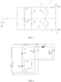
- FIG. 1 is a schematic diagram of a multiplexing circuit 11 of an AC-DC power factor control (PFC) circuit and a battery discharge DC-DC circuit for a single-battery uninterruptible power supply in the conventional technology.
- the multiplexing circuit uses a dual-BOOST circuit topology.
- direct current switches K11 and K12 are opened to isolate a battery B from a mains supply, and the alternating current mains supply performs power factor control on pulse width modulation of a positive-side switching transistor Q11 and a negative-side switching transistor Q12, so that a direct current is output to a positive direct current bus 101 and a negative direct current bus 102.
- the current of the inductor L12 is a continuous direct current, and a circulating current is formed between the inductor L12 and the diode D14, short-circuiting the inductor L12 and allowing a large current to pass through.
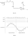
- FIG. 3 shows pulse width modulation control signals and current waveforms of corresponding components when the circuit shown in FIG. 1 is in a battery mode operating state.
- a dashed line range shows an operating situation of the positive half-side, where the positive-side switching transistor Q11 is controlled to perform pulse width modulation, the negative-side switching transistor Q12 is controlled to be in an on state, a current on the inductor L11 is a triangular wave current, a current on the inductor L12 is a substantially constant direct current, and an inductor action is not played, which is equivalent to being shorted.
- the heating of the two inductors is extremely severe, forcing an increase in inductor size, which is a significant drawback.
- such a dual-BOOST circuit topology includes two inductors. During operation in each half cycle in the mains supply mode, only one inductor is involved, resulting in low inductor utilization.
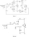
- FIG. 4 is a schematic diagram of a power factor correction (PFC) and DC-DC multiplexing circuit according to an embodiment of the present invention, including: a first mechanical switch RY1, configured to connect the converter to a mains supply; a second mechanical switch RY2, configured to connect the converter to a battery; an inductor L1, one end of which is connected to the mains supply through the first mechanical switch RY1, and connected to a positive electrode of the battery B21 through the second mechanical switch RY2; a first node N1 and a second node N2; a first rectifier bridge arm 213, connected between the first node N1 and the second node N2, where the first rectifier bridge arm 213 has a first intermediate node N3, and the first intermediate node N3 is connected to the other end of the inductor L1; a second rectifier bridge arm 214, connected between the
- a collector namely, a second electrode of a switching transistor Q1 (first semiconductor switch) is connected to the first node N1, and an emitter, namely, a first electrode of the switching transistor Q1 is connected to the second node N2;
- a collector, namely, a second electrode of a switching transistor Q2 (second semiconductor switch) is connected to the second node N2, and an emitter, namely, a first electrode of the switching transistor Q2 is connected to a negative direct current bus 212 serving as an output;
- an anode of a first diode D6 is connected to the first node N1, and a cathode of the first diode D6 is connected to the positive direct current bus 211 serving as another output.
- FIG. 11 shows example pulse width modulation control signals and current waveforms of corresponding components when the circuit shown in FIG. 5 operates in the positive and negative half cycles in the battery mode.
- the switching transistor Q1 is controlled to perform pulse width modulation
- the switching transistor Q2 is controlled to be in an off state
- the switching transistor Q3 is controlled to be in an on state
- a current on the inductor L1 presents a triangular wave current as the switching transistor Q1 is switched on and off, where a rising waveform indicates that the inductor L1 is in a charging state, and a falling waveform indicates that the inductor L1 is in a discharging state.
- the switching transistor Q2 When the battery discharges to supply power to the negative direct current bus, that is, during operation in the negative half cycle, the switching transistor Q2 is controlled to perform pulse width modulation, the switching transistor Q1 is controlled to be in an on state, the switching transistor Q3 is controlled to be in an off state, and a current on the inductor L1 presents a triangular wave current as the switching transistor Q2 is switched on or off.
- a potential difference between the negative electrode of the battery B21 and the neutral point N5 jumps with a level of Q3, the jumping is power frequency jumping, and a frequency is very low.
Landscapes
- Engineering & Computer Science (AREA)
- Power Engineering (AREA)
- Business, Economics & Management (AREA)
- Emergency Management (AREA)
- Physics & Mathematics (AREA)
- Electromagnetism (AREA)
- Rectifiers (AREA)
- Dc-Dc Converters (AREA)
Applications Claiming Priority (1)
| Application Number | Priority Date | Filing Date | Title |
|---|---|---|---|
| CN202311310169.2A CN119813756A (zh) | 2023-10-10 | 2023-10-10 | 功率因数修正与dc-dc复用变换器 |
Publications (2)
| Publication Number | Publication Date |
|---|---|
| EP4539317A1 true EP4539317A1 (fr) | 2025-04-16 |
| EP4539317B1 EP4539317B1 (fr) | 2025-12-17 |
Family
ID=93014808
Family Applications (1)
| Application Number | Title | Priority Date | Filing Date |
|---|---|---|---|
| EP24204940.1A Active EP4539317B1 (fr) | 2023-10-10 | 2024-10-07 | Convertisseur de correction de facteur de puissance et de multiplexage cc-cc |
Country Status (3)
| Country | Link |
|---|---|
| US (1) | US12556083B2 (fr) |
| EP (1) | EP4539317B1 (fr) |
| CN (1) | CN119813756A (fr) |
Citations (3)
| Publication number | Priority date | Publication date | Assignee | Title |
|---|---|---|---|---|
| EP2548286B1 (fr) * | 2010-03-18 | 2016-06-29 | Schneider Electric IT Corporation | Conversion de courant alternatif en courant continu |
| EP2737603B1 (fr) * | 2011-07-28 | 2016-09-14 | Schneider Electric IT Corporation | Topologies d'alimentation par batterie unique pour systèmes ups en ligne |
| EP4239837A1 (fr) * | 2022-02-09 | 2023-09-06 | Lian Zheng Electronic (Shenzhen) Co., Ltd. | Convertisseur de multiplexage cc-cc et de correction de facteur de puissance et alimentation sans coupure le comprenant |
-
2023
- 2023-10-10 CN CN202311310169.2A patent/CN119813756A/zh active Pending
-
2024
- 2024-10-01 US US18/903,128 patent/US12556083B2/en active Active
- 2024-10-07 EP EP24204940.1A patent/EP4539317B1/fr active Active
Patent Citations (3)
| Publication number | Priority date | Publication date | Assignee | Title |
|---|---|---|---|---|
| EP2548286B1 (fr) * | 2010-03-18 | 2016-06-29 | Schneider Electric IT Corporation | Conversion de courant alternatif en courant continu |
| EP2737603B1 (fr) * | 2011-07-28 | 2016-09-14 | Schneider Electric IT Corporation | Topologies d'alimentation par batterie unique pour systèmes ups en ligne |
| EP4239837A1 (fr) * | 2022-02-09 | 2023-09-06 | Lian Zheng Electronic (Shenzhen) Co., Ltd. | Convertisseur de multiplexage cc-cc et de correction de facteur de puissance et alimentation sans coupure le comprenant |
Non-Patent Citations (1)
| Title |
|---|
| FERNANDES LEONARDO GOBEL ET AL: "A half-bridge doubler boost operating as AC-DC and DC-DC converter", 2016 12TH IEEE INTERNATIONAL CONFERENCE ON INDUSTRY APPLICATIONS (INDUSCON), IEEE, 20 November 2016 (2016-11-20), pages 1 - 8, XP033074070, DOI: 10.1109/INDUSCON.2016.7874514 * |
Also Published As
| Publication number | Publication date |
|---|---|
| CN119813756A (zh) | 2025-04-11 |
| US20250119055A1 (en) | 2025-04-10 |
| US12556083B2 (en) | 2026-02-17 |
| EP4539317B1 (fr) | 2025-12-17 |
Similar Documents
| Publication | Publication Date | Title |
|---|---|---|
| US11605967B2 (en) | On-board charger | |
| US10523112B2 (en) | Power converter and method of controlling the same | |
| US12255529B2 (en) | Power factor correction and DC-DC multiplexing converter and uninterruptible power supply including the same | |
| CN104272571B (zh) | 功率转换装置 | |
| CN217788552U (zh) | 电动汽车的电池加热系统以及电动汽车 | |
| WO2021232785A1 (fr) | Appareil à topologie de bras à trois ponts, procédé de commande et système d'alimentation électrique sans coupure | |
| CN103187785B (zh) | 一种ups模块及ups系统 | |
| WO2021232749A1 (fr) | Dispositif topologique à bras en trois ponts et système d'alimentation sans coupure | |
| US12418194B2 (en) | Multiple input converter and an uninterruptible power supply including the same | |
| CN115136443A (zh) | 三桥臂拓扑装置、控制方法、逆变系统及不间断电源系统 | |
| CN111224419A (zh) | 储能逆变器 | |
| CN116961454A (zh) | 母线中点平衡电路、逆变器与储能系统 | |
| CN115694187A (zh) | 一种升压功率变换电路及装置 | |
| CN112865563B (zh) | 一种三端口箝位型的背对背无桥三电平整流器 | |
| EP4539317A1 (fr) | Convertisseur de correction de facteur de puissance et de multiplexage cc-cc | |
| CN118074305A (zh) | 一种不间断电源系统 | |
| CN116914819A (zh) | 一种功率变换装置和光伏储能系统 | |
| CN110224584A (zh) | 家电设备及其无源功率因数校正电路 | |
| CN120016829A (zh) | 功率变换器和包含该功率变换器的ups | |
| CN211352072U (zh) | 变频空调整流电路及变频空调 | |
| US20250392157A1 (en) | Power converters and unnterruptible power supplies (upss) including the same | |
| US20260121524A1 (en) | Direct current (dc)-dc conversion circuits and power conversion circuits including the same | |
| US12476481B2 (en) | Uninterruptible power supply | |
| US20230253879A1 (en) | Charger, a multiplexing current conversion circuit and an uninterruptible power supply including the same | |
| CN222355988U (zh) | 充放电电路以及车辆 |
Legal Events
| Date | Code | Title | Description |
|---|---|---|---|
| PUAI | Public reference made under article 153(3) epc to a published international application that has entered the european phase |
Free format text: ORIGINAL CODE: 0009012 |
|
| STAA | Information on the status of an ep patent application or granted ep patent |
Free format text: STATUS: THE APPLICATION HAS BEEN PUBLISHED |
|
| AK | Designated contracting states |
Kind code of ref document: A1 Designated state(s): AL AT BE BG CH CY CZ DE DK EE ES FI FR GB GR HR HU IE IS IT LI LT LU LV MC ME MK MT NL NO PL PT RO RS SE SI SK SM TR |
|
| STAA | Information on the status of an ep patent application or granted ep patent |
Free format text: STATUS: REQUEST FOR EXAMINATION WAS MADE |
|
| 17P | Request for examination filed |
Effective date: 20250519 |
|
| GRAP | Despatch of communication of intention to grant a patent |
Free format text: ORIGINAL CODE: EPIDOSNIGR1 |
|
| STAA | Information on the status of an ep patent application or granted ep patent |
Free format text: STATUS: GRANT OF PATENT IS INTENDED |
|
| INTG | Intention to grant announced |
Effective date: 20250715 |
|
| GRAS | Grant fee paid |
Free format text: ORIGINAL CODE: EPIDOSNIGR3 |
|
| GRAA | (expected) grant |
Free format text: ORIGINAL CODE: 0009210 |
|
| STAA | Information on the status of an ep patent application or granted ep patent |
Free format text: STATUS: THE PATENT HAS BEEN GRANTED |
|
| P01 | Opt-out of the competence of the unified patent court (upc) registered |
Free format text: CASE NUMBER: UPC_APP_0011330_4539317/2025 Effective date: 20251028 |
|
| RAP3 | Party data changed (applicant data changed or rights of an application transferred) |
Owner name: LIAN ZHENG ELECTRONICS (SHENZHEN) CO., LTD. |
|
| AK | Designated contracting states |
Kind code of ref document: B1 Designated state(s): AL AT BE BG CH CY CZ DE DK EE ES FI FR GB GR HR HU IE IS IT LI LT LU LV MC ME MK MT NL NO PL PT RO RS SE SI SK SM TR |
|
| REG | Reference to a national code |
Ref country code: CH Ref legal event code: F10 Free format text: ST27 STATUS EVENT CODE: U-0-0-F10-F00 (AS PROVIDED BY THE NATIONAL OFFICE) Effective date: 20251217 Ref country code: GB Ref legal event code: FG4D |
|
| REG | Reference to a national code |
Ref country code: DE Ref legal event code: R096 Ref document number: 602024001737 Country of ref document: DE |
|
| REG | Reference to a national code |
Ref country code: LT Ref legal event code: MG9D |
|
| PG25 | Lapsed in a contracting state [announced via postgrant information from national office to epo] |
Ref country code: NO Free format text: LAPSE BECAUSE OF FAILURE TO SUBMIT A TRANSLATION OF THE DESCRIPTION OR TO PAY THE FEE WITHIN THE PRESCRIBED TIME-LIMIT Effective date: 20260317 |
|
| PG25 | Lapsed in a contracting state [announced via postgrant information from national office to epo] |
Ref country code: FI Free format text: LAPSE BECAUSE OF FAILURE TO SUBMIT A TRANSLATION OF THE DESCRIPTION OR TO PAY THE FEE WITHIN THE PRESCRIBED TIME-LIMIT Effective date: 20251217 Ref country code: HR Free format text: LAPSE BECAUSE OF FAILURE TO SUBMIT A TRANSLATION OF THE DESCRIPTION OR TO PAY THE FEE WITHIN THE PRESCRIBED TIME-LIMIT Effective date: 20251217 |
|
| PG25 | Lapsed in a contracting state [announced via postgrant information from national office to epo] |
Ref country code: RS Free format text: LAPSE BECAUSE OF FAILURE TO SUBMIT A TRANSLATION OF THE DESCRIPTION OR TO PAY THE FEE WITHIN THE PRESCRIBED TIME-LIMIT Effective date: 20260317 |