EP4539322A1 - Commande en mode rafale de convertisseurs de puissance résonants - Google Patents
Commande en mode rafale de convertisseurs de puissance résonants Download PDFInfo
- Publication number
- EP4539322A1 EP4539322A1 EP23202296.2A EP23202296A EP4539322A1 EP 4539322 A1 EP4539322 A1 EP 4539322A1 EP 23202296 A EP23202296 A EP 23202296A EP 4539322 A1 EP4539322 A1 EP 4539322A1
- Authority
- EP
- European Patent Office
- Prior art keywords
- pwm
- resonant power
- time periods
- power converter
- time period
- Prior art date
- Legal status (The legal status is an assumption and is not a legal conclusion. Google has not performed a legal analysis and makes no representation as to the accuracy of the status listed.)
- Withdrawn
Links
Images



Classifications
-
- H—ELECTRICITY
- H02—GENERATION; CONVERSION OR DISTRIBUTION OF ELECTRIC POWER
- H02M—APPARATUS FOR CONVERSION BETWEEN AC AND AC, BETWEEN AC AND DC, OR BETWEEN DC AND DC, AND FOR USE WITH MAINS OR SIMILAR POWER SUPPLY SYSTEMS; CONVERSION OF DC OR AC INPUT POWER INTO SURGE OUTPUT POWER; CONTROL OR REGULATION THEREOF
- H02M1/00—Details of apparatus for conversion
- H02M1/0003—Details of control, feedback or regulation circuits
- H02M1/0032—Control circuits allowing low power mode operation, e.g. in standby mode
- H02M1/0035—Control circuits allowing low power mode operation, e.g. in standby mode using burst mode control
-
- H—ELECTRICITY
- H02—GENERATION; CONVERSION OR DISTRIBUTION OF ELECTRIC POWER
- H02M—APPARATUS FOR CONVERSION BETWEEN AC AND AC, BETWEEN AC AND DC, OR BETWEEN DC AND DC, AND FOR USE WITH MAINS OR SIMILAR POWER SUPPLY SYSTEMS; CONVERSION OF DC OR AC INPUT POWER INTO SURGE OUTPUT POWER; CONTROL OR REGULATION THEREOF
- H02M1/00—Details of apparatus for conversion
- H02M1/0048—Circuits or arrangements for reducing losses
- H02M1/0054—Transistor switching losses
- H02M1/0058—Transistor switching losses by employing soft switching techniques, i.e. commutation of transistors when applied voltage is zero or when current flow is zero
-
- H—ELECTRICITY
- H02—GENERATION; CONVERSION OR DISTRIBUTION OF ELECTRIC POWER
- H02M—APPARATUS FOR CONVERSION BETWEEN AC AND AC, BETWEEN AC AND DC, OR BETWEEN DC AND DC, AND FOR USE WITH MAINS OR SIMILAR POWER SUPPLY SYSTEMS; CONVERSION OF DC OR AC INPUT POWER INTO SURGE OUTPUT POWER; CONTROL OR REGULATION THEREOF
- H02M3/00—Conversion of DC power input into DC power output
- H02M3/01—Resonant DC/DC converters
-
- H—ELECTRICITY
- H02—GENERATION; CONVERSION OR DISTRIBUTION OF ELECTRIC POWER
- H02M—APPARATUS FOR CONVERSION BETWEEN AC AND AC, BETWEEN AC AND DC, OR BETWEEN DC AND DC, AND FOR USE WITH MAINS OR SIMILAR POWER SUPPLY SYSTEMS; CONVERSION OF DC OR AC INPUT POWER INTO SURGE OUTPUT POWER; CONTROL OR REGULATION THEREOF
- H02M3/00—Conversion of DC power input into DC power output
- H02M3/22—Conversion of DC power input into DC power output with intermediate conversion into AC
- H02M3/24—Conversion of DC power input into DC power output with intermediate conversion into AC by static converters
- H02M3/28—Conversion of DC power input into DC power output with intermediate conversion into AC by static converters using discharge tubes with control electrode or semiconductor devices with control electrode to produce the intermediate AC
- H02M3/325—Conversion of DC power input into DC power output with intermediate conversion into AC by static converters using discharge tubes with control electrode or semiconductor devices with control electrode to produce the intermediate AC using devices of a triode or a transistor type requiring continuous application of a control signal
- H02M3/335—Conversion of DC power input into DC power output with intermediate conversion into AC by static converters using discharge tubes with control electrode or semiconductor devices with control electrode to produce the intermediate AC using devices of a triode or a transistor type requiring continuous application of a control signal using semiconductor devices only
- H02M3/33569—Conversion of DC power input into DC power output with intermediate conversion into AC by static converters using discharge tubes with control electrode or semiconductor devices with control electrode to produce the intermediate AC using devices of a triode or a transistor type requiring continuous application of a control signal using semiconductor devices only having several active switching elements
- H02M3/33571—Half-bridge at primary side of an isolation transformer
-
- H—ELECTRICITY
- H05—ELECTRIC TECHNIQUES NOT OTHERWISE PROVIDED FOR
- H05B—ELECTRIC HEATING; ELECTRIC LIGHT SOURCES NOT OTHERWISE PROVIDED FOR; CIRCUIT ARRANGEMENTS FOR ELECTRIC LIGHT SOURCES, IN GENERAL
- H05B45/00—Circuit arrangements for operating light-emitting diodes [LED]
- H05B45/30—Driver circuits
- H05B45/32—Pulse-control circuits
- H05B45/327—Burst dimming
-
- H—ELECTRICITY
- H05—ELECTRIC TECHNIQUES NOT OTHERWISE PROVIDED FOR
- H05B—ELECTRIC HEATING; ELECTRIC LIGHT SOURCES NOT OTHERWISE PROVIDED FOR; CIRCUIT ARRANGEMENTS FOR ELECTRIC LIGHT SOURCES, IN GENERAL
- H05B45/00—Circuit arrangements for operating light-emitting diodes [LED]
- H05B45/30—Driver circuits
- H05B45/37—Converter circuits
- H05B45/3725—Switched mode power supply [SMPS]
- H05B45/39—Circuits containing inverter bridges
Definitions
- the present disclosure relates generally to the field of lighting technology, and more particularly to a resonant power converter for a light source, and to a luminaire comprising the same.
- a low-frequency pulse width modulation may be used to implement a burst mode control of a constant load current in accordance with a given dimming level (see FIG. 3 ).
- This non-monotonicity affects an accurate control of the dimming level as well as a compensation of disturbances by a closed-loop control of the constant load current.
- the resonant power converter may further comprise a memory, being configured to provide the successive values of the respective LF-PWM on-time periods T LF , HS ON , T LF , LS ON .
- a control variable such as an on-time period of a control signal 14, 15 of a switch 11, 12
- P proportional
- I integral
- D derivative
- the LF-PWM and HF-PWM may be synchronized.
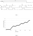
- the LF-PWM on-time period T LF ON can only change by half of the HF-PWM cycle period T HF or more, and that higher resolutions, i.e., smaller steps, will lead to non-monocity.
- the LF-PWM on-time period T LF ON has been changed by less than half of the HF-PWM cycle period T HF , such that the HF-PWM on-time period ⁇ ⁇ T HF ON of the last HF-PWM cycle is truncated by the LF-PWM on-time period T LF ON .
- FIG. 4 illustrates a non-monotonic load current provided by the known burst mode control versus the given on-time period T LF ON .
- a resonant power converter In order for a resonant power converter to have Zero Voltage Switching (ZVS) turning on, it is usually used in inductive mode, so that the resonant current lags with respect to the voltage across the tank and load. This lag causes a negative instantaneous input power. In other words, during each half HF cycle, there exists an interval in which the direction of the instantaneous power is backward, i.e. from the resonant circuit to the source.
- ZVS Zero Voltage Switching
- FIG. 5 illustrates a fixed deadtime based burst mode control in accordance with the present disclosure.
- the control circuit 13 is configured to modulate the control signals 14, 15 of the switches 11, 12 concurrently in accordance with LF-PWM having a cycle period T LF and respective on-time periods T LF , HS ON , T LF , LS OB .
- the control circuit 13 is further configured to modulate the control signals 14, 15 of the switches 11, 12 alternatingly in accordance with HF-PWM having a cycle period T HF , a full on-time period T HF ON and a truncated on-time period ⁇ ⁇ T HF ON being truncated in accordance with the LF-PWM.
- the LF-PWM and HF-PWM may be synchronized.
- the full HF-PWM on-time periods T HF ON as well as the truncated HF-PWM on-time periods ⁇ ⁇ T HF ON of the modulated control signals 14, 15 may mutually be spaced by half of the HF-PWM cycle period T HF minus the full HF-PWM on-time period T HF ON (" fixed deadtime ").
- the LF-PWM on-time periods T LF , HS ON , T LF , LS ON of the modulated control signals 14, 15 may thus differ by the truncated HF-PWM on-time period ⁇ ⁇ T HF ON plus half of the HF-PWM cycle period T HF minus the full HF-PWM on-time period T HF ON .
- FIG. 6 illustrates a fixed frequency based burst mode control in accordance with the present disclosure.
- control circuit 13 is configured to modulate the control signals 14, 15 of the switches 11, 12 concurrently in accordance with LF-PWM having the cycle period T LF and the respective on-time periods T LF , HS ON , T LF , LS ON .
- control circuit 13 is configured to modulate the control signals 14, 15 of the switches 11, 12 alternatingly in accordance with HF-PWM having a cycle period T HF , the full on-time period T HF ON and the truncated on-time period ⁇ ⁇ T HF ON being truncated in accordance with the LF-PWM.
- the LF-PWM and HF-PWM may be synchronized.
- the LF-PWM on-time periods T LF , HS ON , T LF , LS ON of the modulated control signals 14, 15 may thus differ by half of the HF-PWM cycle period T HF .
- FIG. 7 illustrates a chirped frequency based burst mode control in accordance with the present disclosure.
- control circuit 13 is configured to modulate the control signals 14, 15 of the switches 11, 12 alternatingly in accordance with HF-PWM having a cycle period T HF , the full on-time period T HF ON and the truncated on-time period ⁇ ⁇ T HF ON being truncated in accordance with the LF-PWM.
- the truncated HF-PWM on-time periods ⁇ ⁇ T HF ON of the modulated control signals 14, 15 may mutually be shifted by half of the HF-PWM cycle period T HF minus a stepwise adjustable time period n ⁇ ⁇ t ( "chirped frequency" ) .
- the LF-PWM on-time periods T LF , HS ON , T LF , LS ON of the modulated control signals 14, 15 may thus differ by the truncated HF-PWM on-time period ⁇ ⁇ T HF ON plus half of the HF-PWM cycle period T HF minus the stepwise adjustable time period n ⁇ ⁇ t.
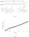
- FIG. 8 illustrates a monotonic load current provided by the chirped frequency based burst mode control versus the given on-time period T LF ON .
- integration over the last HF cycle yields positive values which increase the transmitted average (output) power due to HF-PWM such that the depicted black monotonic curve of the load power is obtained.
- the grey non-monotonic curve of FIG. 4 as a reference representing ordinary LF-PWM, wherein the integral over ⁇ may yield a negative value, depending on ⁇ (i.e., the HF-PWM on-time period ⁇ ⁇ T HF ON of the last HF-PWM cycle being truncated by the LF-PWM on-time period T LF ON ).
- FIG. 9 illustrates a fixed frequency based burst mode control featuring pulse frequency modulation, in accordance with the present disclosure.
- the control circuit 13 may further be configured to modulate the control signals 14, 15 of the switches 11, 12 concurrently in accordance with low-frequency pulse frequency modulations (LF-PFM) having a stepwise adjustable off-time period T LF OFF between successive values of the respective LF-PWM on-time periods T LF , HS ON , T LF , LS ON .
- LF-PFM low-frequency pulse frequency modulations
- off-time period T LF OFF may also undergo stepwise adjustment in terms of a decrease as well.
- the memory 16 mentioned in connection with FIGs. 1, 2 may be configured to provide the successive values of the respective LF-PWM on-time periods T LF , HS ON , T LF , LS ON .
- a computer program may be stored/distributed on a suitable medium, such as an optical storage medium or a solid-state medium supplied together with or as part of other hardware, but may also be distributed in other forms, such as via the Internet or other wired or wireless telecommunication systems.
- a suitable medium such as an optical storage medium or a solid-state medium supplied together with or as part of other hardware, but may also be distributed in other forms, such as via the Internet or other wired or wireless telecommunication systems.
Landscapes
- Engineering & Computer Science (AREA)
- Power Engineering (AREA)
- Dc-Dc Converters (AREA)
Priority Applications (2)
| Application Number | Priority Date | Filing Date | Title |
|---|---|---|---|
| EP23202296.2A EP4539322A1 (fr) | 2023-10-09 | 2023-10-09 | Commande en mode rafale de convertisseurs de puissance résonants |
| PCT/EP2024/077558 WO2025078206A1 (fr) | 2023-10-09 | 2024-10-01 | Commande en mode rafale de convertisseurs de puissance résonants |
Applications Claiming Priority (1)
| Application Number | Priority Date | Filing Date | Title |
|---|---|---|---|
| EP23202296.2A EP4539322A1 (fr) | 2023-10-09 | 2023-10-09 | Commande en mode rafale de convertisseurs de puissance résonants |
Publications (1)
| Publication Number | Publication Date |
|---|---|
| EP4539322A1 true EP4539322A1 (fr) | 2025-04-16 |
Family
ID=88296965
Family Applications (1)
| Application Number | Title | Priority Date | Filing Date |
|---|---|---|---|
| EP23202296.2A Withdrawn EP4539322A1 (fr) | 2023-10-09 | 2023-10-09 | Commande en mode rafale de convertisseurs de puissance résonants |
Country Status (2)
| Country | Link |
|---|---|
| EP (1) | EP4539322A1 (fr) |
| WO (1) | WO2025078206A1 (fr) |
Citations (3)
| Publication number | Priority date | Publication date | Assignee | Title |
|---|---|---|---|---|
| US20100020570A1 (en) * | 2008-07-25 | 2010-01-28 | Melanson John L | Resonant switching power converter with burst mode transition shaping |
| US20140312789A1 (en) * | 2013-04-23 | 2014-10-23 | Virginia Tech Intellectual Properties, Inc. | Optimal Trajectory Control for LLC Resonant Converter for LED PWM Dimming |
| US20150084544A1 (en) * | 2012-03-21 | 2015-03-26 | Tridonic Gmbh & Co Kg | Operating circuit for leds, having dimming signal comprising high-frequency modulated pulse packet signal with harmonized frequencies |
-
2023
- 2023-10-09 EP EP23202296.2A patent/EP4539322A1/fr not_active Withdrawn
-
2024
- 2024-10-01 WO PCT/EP2024/077558 patent/WO2025078206A1/fr active Pending
Patent Citations (3)
| Publication number | Priority date | Publication date | Assignee | Title |
|---|---|---|---|---|
| US20100020570A1 (en) * | 2008-07-25 | 2010-01-28 | Melanson John L | Resonant switching power converter with burst mode transition shaping |
| US20150084544A1 (en) * | 2012-03-21 | 2015-03-26 | Tridonic Gmbh & Co Kg | Operating circuit for leds, having dimming signal comprising high-frequency modulated pulse packet signal with harmonized frequencies |
| US20140312789A1 (en) * | 2013-04-23 | 2014-10-23 | Virginia Tech Intellectual Properties, Inc. | Optimal Trajectory Control for LLC Resonant Converter for LED PWM Dimming |
Non-Patent Citations (1)
| Title |
|---|
| FENG WEIYI ET AL: "Optimal Trajectory Control of LLC Resonant Converters for LED PWM Dimming", IEEE TRANSACTIONS ON POWER ELECTRONICS, INSTITUTE OF ELECTRICAL AND ELECTRONICS ENGINEERS, USA, vol. 29, no. 2, 1 February 2014 (2014-02-01), pages 979 - 987, XP011524645, ISSN: 0885-8993, [retrieved on 20130820], DOI: 10.1109/TPEL.2013.2257864 * |
Also Published As
| Publication number | Publication date |
|---|---|
| WO2025078206A1 (fr) | 2025-04-17 |
Similar Documents
| Publication | Publication Date | Title |
|---|---|---|
| EP2214457B1 (fr) | Appareil de gradation de del | |
| NL193647C (nl) | Ontsteekketen voor een ontladingslamp van een voertuig. | |
| EP2294898B1 (fr) | Dispositif de commande pour commander un ensemble del, application d'éclairage et procédé de commande d'un ensemble del | |
| US8786208B2 (en) | Electronic device for driving light emitting diodes | |
| JP5693870B2 (ja) | スイッチング電源回路 | |
| US10622894B2 (en) | Synchronous converter | |
| JP6483749B2 (ja) | 調光駆動回路及びその制御方法 | |
| US20110234122A1 (en) | Circuitry for driving light emitting diodes and associated methods | |
| CN101631411A (zh) | Led驱动器的动态净空控制 | |
| US10251227B2 (en) | Clocked electronic energy converter | |
| CN111182676B (zh) | 调光电路及调光控制方法 | |
| JP6516311B2 (ja) | 固体照明要素の少なくとも2つのセットを駆動するためのドライバ及び方法 | |
| WO2025078206A1 (fr) | Commande en mode rafale de convertisseurs de puissance résonants | |
| FI125106B (en) | PWM anthems | |
| US11895749B2 (en) | Light emitting diode (LED) drive method and circuit, and LED lighting device | |
| US9585204B2 (en) | Driving circuit and control method thereof | |
| JP7199014B2 (ja) | 照明手段アセンブリの作動装置および作動方法 | |
| JP2012195251A (ja) | Led駆動回路 | |
| EP4135480B1 (fr) | Pilote de del doté d'une correction aval auto-réglable | |
| US6781324B2 (en) | Ballast for at least one electric incandescent lamp | |
| EP4462665A1 (fr) | Convertisseur résonant commuté côté primaire isolé amélioré pour fournir une charge de del | |
| EP4525280A1 (fr) | Convertisseur indirect hybride résonant, et agencement de commande et son procédé de fonctionnement | |
| WO2013047401A1 (fr) | Circuit d'excitation de del |
Legal Events
| Date | Code | Title | Description |
|---|---|---|---|
| PUAI | Public reference made under article 153(3) epc to a published international application that has entered the european phase |
Free format text: ORIGINAL CODE: 0009012 |
|
| STAA | Information on the status of an ep patent application or granted ep patent |
Free format text: STATUS: THE APPLICATION HAS BEEN PUBLISHED |
|
| AK | Designated contracting states |
Kind code of ref document: A1 Designated state(s): AL AT BE BG CH CY CZ DE DK EE ES FI FR GB GR HR HU IE IS IT LI LT LU LV MC ME MK MT NL NO PL PT RO RS SE SI SK SM TR |
|
| STAA | Information on the status of an ep patent application or granted ep patent |
Free format text: STATUS: THE APPLICATION IS DEEMED TO BE WITHDRAWN |
|
| 18D | Application deemed to be withdrawn |
Effective date: 20251017 |