EP4539400A1 - Dispositif et procédé d'edge computing et système de l'internet des objets - Google Patents
Dispositif et procédé d'edge computing et système de l'internet des objets Download PDFInfo
- Publication number
- EP4539400A1 EP4539400A1 EP22948241.9A EP22948241A EP4539400A1 EP 4539400 A1 EP4539400 A1 EP 4539400A1 EP 22948241 A EP22948241 A EP 22948241A EP 4539400 A1 EP4539400 A1 EP 4539400A1
- Authority
- EP
- European Patent Office
- Prior art keywords
- data
- time base
- memory
- base signal
- state machine
- Prior art date
- Legal status (The legal status is an assumption and is not a legal conclusion. Google has not performed a legal analysis and makes no representation as to the accuracy of the status listed.)
- Pending
Links
Images




Classifications
-
- H—ELECTRICITY
- H04—ELECTRIC COMMUNICATION TECHNIQUE
- H04L—TRANSMISSION OF DIGITAL INFORMATION, e.g. TELEGRAPHIC COMMUNICATION
- H04L12/00—Data switching networks
- H04L12/02—Details
- H04L12/12—Arrangements for remote connection or disconnection of substations or of equipment thereof
-
- G—PHYSICS
- G05—CONTROLLING; REGULATING
- G05B—CONTROL OR REGULATING SYSTEMS IN GENERAL; FUNCTIONAL ELEMENTS OF SUCH SYSTEMS; MONITORING OR TESTING ARRANGEMENTS FOR SUCH SYSTEMS OR ELEMENTS
- G05B19/00—Program-control systems
- G05B19/02—Program-control systems electric
- G05B19/04—Program control other than numerical control, i.e. in sequence controllers or logic controllers
- G05B19/042—Program control other than numerical control, i.e. in sequence controllers or logic controllers using digital processors
- G05B19/0421—Multiprocessor system
-
- G—PHYSICS
- G05—CONTROLLING; REGULATING
- G05B—CONTROL OR REGULATING SYSTEMS IN GENERAL; FUNCTIONAL ELEMENTS OF SUCH SYSTEMS; MONITORING OR TESTING ARRANGEMENTS FOR SUCH SYSTEMS OR ELEMENTS
- G05B19/00—Program-control systems
- G05B19/02—Program-control systems electric
- G05B19/04—Program control other than numerical control, i.e. in sequence controllers or logic controllers
- G05B19/05—Programmable logic controllers, e.g. simulating logic interconnections of signals according to ladder diagrams or function charts
-
- H—ELECTRICITY
- H04—ELECTRIC COMMUNICATION TECHNIQUE
- H04L—TRANSMISSION OF DIGITAL INFORMATION, e.g. TELEGRAPHIC COMMUNICATION
- H04L67/00—Network arrangements or protocols for supporting network services or applications
- H04L67/01—Protocols
- H04L67/12—Protocols specially adapted for proprietary or special-purpose networking environments, e.g. medical networks, sensor networks, networks in vehicles or remote metering networks
-
- H—ELECTRICITY
- H04—ELECTRIC COMMUNICATION TECHNIQUE
- H04W—WIRELESS COMMUNICATION NETWORKS
- H04W4/00—Services specially adapted for wireless communication networks; Facilities therefor
- H04W4/30—Services specially adapted for particular environments, situations or purposes
- H04W4/38—Services specially adapted for particular environments, situations or purposes for collecting sensor information
-
- H—ELECTRICITY
- H04—ELECTRIC COMMUNICATION TECHNIQUE
- H04W—WIRELESS COMMUNICATION NETWORKS
- H04W4/00—Services specially adapted for wireless communication networks; Facilities therefor
- H04W4/70—Services for machine-to-machine communication [M2M] or machine type communication [MTC]
Definitions
- the present application relates to the field of Internet of Things (IoT) technology, and more specifically to an edge computing device, method, and IoT system.
- IoT Internet of Things
- the present disclosure provides an edge computing device that facilitates interaction between a user and multiple field devices.
- an edge computing device which includes a processing unit and a programmable logic unit, wherein the programmable logic unit comprises a first memory, a second memory, an instruction distribution module, and a data acquisition module, wherein the processing unit receives instructions from the cloud and writes these instructions into the first memory, and reads data from the second memory sent from field devices, then sends the data to the cloud; the instruction distribution module reads the instructions from the first memory and sends them to corresponding field devices.
- the data acquisition module collects data from the field devices and stores them in the second memory; the programmable logic unit generates periodic first time base signals and second time base signals, respectively, and the instruction distribution module is designed to have a first state machine, and the data acquisition module is designed to have a second state machine such that in the downlink direction, the processing unit, the first memory, and the instruction distribution module perform downlink instruction distribution based on the first time base signals and the first state machine; in the uplink direction, the processing unit, the second memory, and the data acquisition module perform uplink data transmission based on the second time base signals and the second state machine.
- multiple field devices can be connected to cloud services, and status information from all field devices can be collected.
- user instructions from the cloud or any other cloud-connected devices can be sent to specific field devices, enabling a user to interact with multiple field devices.
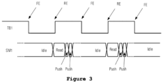
- the processing unit starts writing instructions from the cloud into the first memory, and the write operation ends at a specific moment during the low level of the current cycle of the first time base signal, during which the first state machine of the instruction distribution module is in an idle state; at the next rising edge of the first time base signals, the instruction distribution module starts reading instructions from the first memory and buffering them in a first buffer, and the first state machine is in the reading state; next, the instruction distribution module sequentially distributes the buffered instructions from the first buffer to the corresponding field devices, and the first state machine is in the distributing state; after all the instructions have been distributed, the state machine enters the idle state and waits for the next cycle to enter the reading state.
- the processing unit begins reading data of the previous cycle from the second memory, the read operation ends at a specific moment during the high level of the current cycle, and the processing unit sends the data to the cloud; during this high-level period, the data acquisition module collects data from all field devices and stores them in a second buffer, and the second state machine is in the data collection state; starting from the falling edge during the high-level period of the second time base signals, the data acquisition module writes the buffered data from the second buffer into the second memory; the second state machine is in the data writing state; after the writing operation ends, the second state machine enters the idle state and waits for the next cycle to enter the data collection state.
- the design of the state machines enables the processing unit and programmable logic unit to access the memory under the control of the time base signals.
- the time base signals are configurable by the user, allowing the state data of the edge device and user instructions from the cloud to be transmitted at a configured updating rate.
- the first time base signal and the second time base signal are periodic square wave signals, and their periods may be equal or unequal.
- the time base signals are user-configurable, enabling edge device state data and user instructions from the cloud to be sent at configured update rates.
- the IoT master control unit communicates with the cloud using the MQTT protocol.
- the first memory and the second memory are dual-port block memories.
- an edge computing method comprising: in the downlink direction, receiving instructions from the cloud, writing the instructions into the first memory, reading the instructions from the first memory, and sending the instructions to the corresponding field devices; in the uplink direction, collecting data from the field devices, storing the data in the second memory, reading the data from the second memory, and sending the data to the cloud, wherein in the downlink direction, the instruction distribution is implemented based on the first time base signal and the first state machine; in the uplink direction, the data transmission is implemented based on the second time base signal and the second state machine.
- an IoT system comprising: a cloud, field devices, and the edge computing device described above, wherein the cloud and the field devices communicate through the edge computing device.
- the edge computing device of the present disclosure can preprocess the data collected from the field devices.
- the edge computing device includes both a serial computing structure, i.e., a processing unit, and a parallel computing structure, i.e., a programmable logic unit.
- the processing unit is dedicated to serial computations, e.g., multiplication and accumulation;
- the programmable logic unit is dedicated to parallel computations, e.g., multi-stage pipeline calculations.
- computational resources can be reasonably allocated and utilized based on different requirements for real-time performance and latency, enabling optimal processing of the collected data.
- An MCU chip is generally used to control and process data from sensors, thereby producing an MCU-based IoT field device unit, such as a smart sensor unit (Daniel Sygnat, Johannes Baumer, Cost Improved Intelligent Sensor, US20210123176 ), a fault detection unit (Fang Z, Huang Z, Zhu Y, Detector Temperature Control and Fault Detection System, CN112965550-A ), a vehicle speed detection unit (Sumit Jaiswal, Rajiv Chithambaran, Intelligent Transportation System, Host Processor Vehicle and Method, US20180069724 A1 ), and a power conversion unit (Hayashi Y, Power Conversion Device, US 11063526 B2 ).
- a smart sensor unit Dianiel Sygnat, Johannes Baumer, Cost Improved Intelligent Sensor, US20210123176
- a fault detection unit Fang Z, Huang Z, Zhu Y, Detector Temperature Control and Fault Detection System, CN112965550-A
- MCU-based IoT field device units are combined or cascaded to form a huge network.
- smart sensor units are combined to form a smart home system; fault detection units are combined to form a maintenance system; speed detection units are combined to form an intelligent transportation system; and power conversion units are combined and cascaded to form a smart grid system.
- fault detection units are combined to form a maintenance system; speed detection units are combined to form an intelligent transportation system; and power conversion units are combined and cascaded to form a smart grid system.
- the original state data grows increasingly large. Cloud computing becomes a reasonable method for processing massive amounts of data.
- each unit has an MCU as its own controller, treating all MCUs as edge computing nodes is not meaningful.
- an edge computing device that can interact with multiple IoT field device units.
- state data from multiple units can be collected, preprocessed, and sent to the cloud for processing; on the other hand, users can send instructions to specific units via the cloud.
- an MCU-based IoT field device unit will be referred to as a field device, which uses an MCU as a controller to collect field data.
- the field devices can be various sensors, power converters, etc.
- FIG. 1 is a schematic diagram of the IoT system according to an embodiment of the present disclosure.
- the IoT system 100 includes a cloud 102, an edge computing device 200, and multiple field devices 104, and communication between the cloud 102 and the edge computing device 200 can be achieved through an IoT control unit 106, while communication between the edge computing device 200 and the field devices 104 is conducted via a communication interface 108.
- the IoT control unit 106 can receive user instructions from the cloud 102 using the MQTT (Message Queuing Telemetry Transport) protocol and send instructions to the edge computing device 200 via the SPI (Serial Peripheral Interface) protocol or any other inter-chip communication protocol.
- MQTT Message Queuing Telemetry Transport
- SPI Serial Peripheral Interface
- User instructions may come from the cloud or other user terminal devices connected to the cloud, such as smartphones, tablets, etc.
- the communication interface 108 between the edge computing device 200 and the field devices 104 can use various communication methods such as fiber optic communication, Bluetooth communication, or wireless communication for encoding and decoding.
- the edge computing device 200 can be seen as a bridge between the cloud 102 and multiple field devices 104.
- the core tasks of the edge computing device include instruction transmission, data collection, and data preprocessing.
- the structure and operation of the edge computing device 200 will be explained in detail below by referring to Figure 2 .
- Figure 2 is a block diagram of an exemplary configuration of the edge computing device 200 according to an embodiment of the present disclosure.
- the edge computing device 200 includes a processing unit PS and a programmable logic unit PL.
- the main component of the processing unit PS is a CPU, and the processing unit primarily performs serial computation.
- the programmable logic unit PL is implemented using programmable logic devices, such as FPGA, CPLD, HDPLD, etc. Those skilled in the art can select an appropriate type of device as needed, and the technical solutions disclosed herein do not restrict the specific type of programmable logic device.
- the programmable logic unit is mainly used for parallel computation.
- the programmable logic unit PL includes a first memory BRAM1, a second memory BRAM2, an instruction distribution module CD, and a data collection module DC.
- the processing unit PS is used to receive instructions from the cloud 102 and write these instructions into the first memory BRAM1.
- the instruction distribution module CD reads instructions from the first memory BRAM1 and sends the instructions to the corresponding field devices 104.
- the data collection module DC collects data from the field devices 104 and stores the data in the second memory BRAM2; the processing unit PS reads the data from the field devices 104 from the second memory BRAM2 and sends said data to the cloud 102.
- the CPU in the processing unit PS reads data from the second memory BRAM2 at a fixed frequency so that the processing unit can send the data to the IoT control unit via the SPI communication protocol or any other inter-chip communication protocol at a specific frequency, and then the IoT control unit can send the data from all field devices to the cloud via the MQTT protocol.
- the programmable logic unit PL generates periodic first time base signals TB1 and second time base signals TB2.
- a first state machine SM1 is provided in the instruction distribution module CD
- a second state machine SM2 is provided in the data collection module DC, so that, in the downlink direction, the processing unit PS, the first memory BRAM1, and the instruction distribution module CD implement downlink instruction distribution based on the first time base signal TB1 and the first state machine SM1, and, in the uplink direction, the processing unit PS, the second memory BRAM2, and the data collection module DC implement uplink data transmission based on the second time base signal TB2 and the second state machine SM2.
- the first memory and the second memory can be a dual-port block memory or any other memory capable of reading and writing.
- Figure 3 shows a timing diagram of the instruction distribution mechanism in the instruction distribution module CD of the edge computing device according to an embodiment of the present disclosure.
- the processing unit PS, the first memory BRAM1, and the instruction distribution module CD implement downlink instruction distribution based on the first time base signal TB1 and the first state machine SM1.
- the processing unit PS begins writing instructions from the cloud 102 into the first memory BRAM1, the write operation ends at a moment during the low level of the current cycle of the first time base signal TB1, and, during this process, the first state machine SM1 of the instruction distribution module CD is in the idle state Idle; at the next rising edge RE of the first time base signal TB1, the instruction distribution module CD begins reading instructions from the first memory BRAM1 and buffering the instructions in a first buffer (not shown in the figure), and the first state machine SM1 enters the read state Read; next, the instruction distribution module CD sequentially distributes the buffered instructions from the first buffer to the corresponding field devices, and the first state machine SM1 enters the push state Push; after all instructions are distributed, the first state machine SM1 goes into the idle state Idle and waits to enter the read state for the next cycle.
- the instruction distribution module CD repeatedly executes the operation of distributing instructions from the cloud to each field device. Users can set an appropriate cycle for the first time base signal TB1 to adjust the frequency of instruction distribution as needed.
- Figure 4 shows a timing diagram of the data collection mechanism in the data collection module DC.
- the processing unit PS, the second memory BRAM2, and the data collection module DC implement uplink data transmission based on the second time base signal TB2 and the second state machine SM2.
- the processing unit PS begins reading the data of the previous cycle from the second memory BRAM2, the read operation ends at a moment during the high level of the current cycle, and the processing unit PS sends the data to the cloud; during the high-level period, the data collection module DC collects data from all field devices and buffers the data in a second buffer (not shown in the figure), and the second state machine SM2 is in the data collection state Collect; starting from the falling edge FE of the high-level period of the second time base signal TB2, the data collection module DC writes the buffered data from the second buffer into the second memory BRAM2, and the second state machine SM2 is in the data write state Written; after the write operation ends, the second state machine goes into the idle state Idle and waits to enter the data collection state for the next cycle.
- the data collection module DC repeatedly executes the operation of collecting data from each field device.
- a user can adjust the cycle of the second time base signal TB2 according to the data volume of the field devices to set the data updating frequency.
- the cycle of the second time base signal TB2 may be equal to or different from the cycle of the first time base signal TB1.
- Figure 5 explains how instructions from the cloud are distributed and stored in the first memory by using power converters as examples of field devices.
- the field devices are multiple power converters, each having two stages; the first stage uses an NPC (Neutral Point Clamped) structure to implement the AC-DC function, and the second stage uses a CLLC (two inductors and two capacitors) structure to implement the DC-DC function.
- the instruction content (Content) for converter 0C0 is stored at the address with offsets 0-4, i.e., Offset0-Offset4, the instruction content for converter 1C1 is stored at the address with offsets 5-9, i.e., Offset5-Offset9, and the instruction content for converter 2 can be stored at the address with offsets 10-14 Offset10-Offset14 (not shown in the figure), and so on.
- the first instruction C01 of converter C0 represents an NPC instruction, including an NPC control mode, reset signals, enable signals, precharge instructions, voltage settings, and other information.
- the second instruction C02 is a CLLC instruction, including a CLLC control module, power flow direction, enable signals, voltage settings, current settings, and other information.
- the next three addresses are reserved for future use.
- For each instruction there is a corresponding identifier ID0-ID4 to indicate the type of instruction data. Instructions for other converters follow the same pattern.
- Figure 6 illustrates the memory allocation mechanism in the first memory for general field devices. Figure 6 is similar to Figure 5 . Offset0-Offset9... represent offset addresses, and U0, U1...
- Each field device has a fixed address span.
- the address span in Figure 6 is 5, but it can be configured to any other length based on the number of user instructions.
- the first, second, and third instructions for a field device are arranged sequentially in that address span.
- Figure 7 uses power converters as an example to illustrate how the data collected from power converters are allocated and stored in the second memory.
- this example considers the power converters to have an NPC and CLLC two-stage structure for AC-DC and DC-DC conversion.
- the state data of converter 0C0 are stored at addresses with offsets 0-9, i.e., Offset0-Offset9.
- the state data of converter 1C1 are stored at addresses with offsets 10-19, i.e., Offset0-Offset9.
- the state data of converter 2 are stored at addresses with offsets 20-29 (not shown in the figure), and so on.
- NPC state data include DC voltage value, active current value, reactive current value, error codes, output vector, etc., and are stored at addresses identified as ID0, ID1, ID2, and ID3.
- CLLC state data include DC voltage value, high-side current, low-side current, error status, etc., and are stored at addresses identified as ID4, ID5, ID6, and ID7. Addresses identified as ID8 and ID9 are reserved for future use for structures other than NPC and CLLC structures.
- Figure 8 illustrates the memory allocation mechanism in the second memory for general field devices.
- Figure 8 is similar to Figure 7 .
- Offset0-Offset19... represent offset addresses, and U0, U1... represent field devices.
- the data collected from all field devices U01, U02, ... U19... are arranged sequentially in memory addresses, one after another.
- Each field device has a fixed address span.
- the address span in Figure 8 is 10, but a user can configure the address span to any other length based on the data volume collected from the field devices.
- For each field device multiple sensed parameters can be included.
- edge computing device In the above embodiments, it is apparent that certain processes or methods have also been disclosed. In the following, an overview of these methods is provided without repeating certain details that have already been discussed above. However, it should be noted that, while these methods are disclosed during the description of the edge computing device, these methods do not necessarily use the above-mentioned components or are not necessarily executed by these components. For example, the implementation of the edge computing device may be partially or entirely realized using hardware and/or firmware. The edge computing methods discussed below can also be fully implemented using computer-executable programs, although these methods can also use the hardware and/or firmware of a data relay device.
- Figure 9 is a flowchart illustrating an exemplary process of the edge computing method 900 according to an embodiment of the present disclosure.
- instruction distribution is implemented based on the first time base signal TB1 and the first state machine SM1.
- data transmission is implemented based on the second time base signal TB2 and the second state machine SM2.
- the first time base signal and the second time base signal can be respectively generated by a programmable logic controller for the downlink and uplink.
- implementing downlink instruction distribution based on the first time base signal TB1 and the first state machine SM1 includes the following: Starting from each falling edge of the first time base signal TB1, the instructions from the cloud 102 are written into the first memory BRAM1, and the write operation ends at a moment during the low level of the current cycle of the first time base signal TB1. During this process, the first state machine SM1 is in the idle state Idle. At the next rising edge of the first time base signal TB1, the instructions are read from the first memory BRAM1 and buffered in the first buffer. The first state machine SM1 is in the read state Read. Next, the instructions buffered in the first buffer are sequentially distributed to the corresponding field devices 104. The first state machine (SM1) goes into the push state Push. After all the instructions are distributed, the first state machine goes into the idle state Idle and waits to enter the read state (Read) for the next cycle.
- uplink data transmission based on the second time base signal TB2 and the second state machine SM2 includes the following:
- the edge computing device, method, and IoT system disclosed herein offer one or more of the following advantages:
- the edge computing device according to the present disclosure employs two dual-port block memories and is designed to have one state machine each in the instruction distribution module and the data collection module, respectively, to enable simultaneous transmission of uplink and downlink data.
- Two memories are used as the data exchange medium between the processing unit and the programmable logic unit.
- the processing unit is connected to the cloud through the IoT control unit. In this way, users can access, analyze, and control a large number of field devices through the cloud.
- the edge computing device allows multiple field devices to connect to cloud services and collect state information from all field devices.
- user instructions from the cloud or any other cloud-connected devices can be sent to specific field devices to realize interaction between users and multiple field devices.
- the design of the state machine allows the processing unit and the programmable logic unit to alternately access the memory under the control of the time base signal.
- the time base signal can be configured by the user so that the state data from the edge device and the user instructions from the cloud can be transmitted at configured update rates.
- the edge computing device can preprocess the data collected from field devices.
- the edge computing device includes both a serial computing structure, i.e., the processing unit, and a parallel computing structure, i.e., the programmable logic unit.
- the processing unit is dedicated to serial computations, such as multiplication and accumulation; the programmable logic unit is dedicated to parallel computations, such as pipeline computations. This allows for the rational allocation and utilization of computing resources to achieve optimal computation based on different needs.
- hardware modules can be implemented mechanically or electrically.
- a hardware module may include permanently dedicated circuits or logic (such as dedicated processors, FPGAs, or ASICs) to perform corresponding operations.
- Hardware modules may also include programmable logic or circuits (such as general-purpose processors or other programmable processors) that can be temporarily configured by software to perform corresponding operations.
- the specific implementation method mechanical means, permanently dedicated circuits, or temporarily configured circuits
Landscapes
- Engineering & Computer Science (AREA)
- Signal Processing (AREA)
- Computer Networks & Wireless Communication (AREA)
- General Physics & Mathematics (AREA)
- Physics & Mathematics (AREA)
- Health & Medical Sciences (AREA)
- Automation & Control Theory (AREA)
- Computing Systems (AREA)
- General Health & Medical Sciences (AREA)
- Medical Informatics (AREA)
- Arrangements For Transmission Of Measured Signals (AREA)
- Theoretical Computer Science (AREA)
- Telephonic Communication Services (AREA)
- General Engineering & Computer Science (AREA)
Applications Claiming Priority (1)
| Application Number | Priority Date | Filing Date | Title |
|---|---|---|---|
| PCT/CN2022/101658 WO2024000117A1 (fr) | 2022-06-27 | 2022-06-27 | Dispositif et procédé d'edge computing et système de l'internet des objets |
Publications (2)
| Publication Number | Publication Date |
|---|---|
| EP4539400A1 true EP4539400A1 (fr) | 2025-04-16 |
| EP4539400A4 EP4539400A4 (fr) | 2026-03-04 |
Family
ID=89383660
Family Applications (1)
| Application Number | Title | Priority Date | Filing Date |
|---|---|---|---|
| EP22948241.9A Pending EP4539400A4 (fr) | 2022-06-27 | 2022-06-27 | Dispositif et procédé d'edge computing et système de l'internet des objets |
Country Status (4)
| Country | Link |
|---|---|
| US (1) | US20250390428A1 (fr) |
| EP (1) | EP4539400A4 (fr) |
| CN (1) | CN119452603A (fr) |
| WO (1) | WO2024000117A1 (fr) |
Family Cites Families (17)
| Publication number | Priority date | Publication date | Assignee | Title |
|---|---|---|---|---|
| US6661340B1 (en) * | 2001-04-24 | 2003-12-09 | Microstrategy Incorporated | System and method for connecting security systems to a wireless device |
| US9349262B2 (en) * | 2013-03-15 | 2016-05-24 | Vivint, Inc. | Security system providing a localized humanly-perceivable alert for identifying a facility to emergency personnel |
| CN103970701B (zh) * | 2014-05-28 | 2017-08-25 | 吉林大学 | 基于现场可编程门阵列的数据实时同步采集的知识产权核 |
| US10324773B2 (en) * | 2015-09-17 | 2019-06-18 | Salesforce.Com, Inc. | Processing events generated by internet of things (IoT) |
| US10754334B2 (en) * | 2016-05-09 | 2020-08-25 | Strong Force Iot Portfolio 2016, Llc | Methods and systems for industrial internet of things data collection for process adjustment in an upstream oil and gas environment |
| EP3291200A1 (fr) | 2016-09-05 | 2018-03-07 | Nxp B.V. | Système de transport intelligent, processeur hôte, véhicule et procédé associé |
| US10313914B2 (en) * | 2017-03-13 | 2019-06-04 | Verizon Patent And Licensing Inc. | System and method for registration, monitoring, and notifications regarding groups of internet-of-things (IoT) devices |
| US11095538B2 (en) * | 2018-01-31 | 2021-08-17 | ImageKeeper LLC | Synchronization of data collected by internet of things (IOT) devices |
| WO2019157364A1 (fr) * | 2018-02-09 | 2019-08-15 | Plex Systems, Inc. | Architecture intégrée utilisant une communication entre processeurs et une base de données en mémoire pour la création rapide de convertisseurs de protocoles industriels |
| EP3611579A1 (fr) * | 2018-08-13 | 2020-02-19 | Siemens Aktiengesellschaft | Dispositif d'automatisation en temps réel doté d'un bus de données en temps réel |
| JP7328748B2 (ja) | 2018-10-22 | 2023-08-17 | 株式会社東芝 | 電力変換装置 |
| DE102019007379A1 (de) | 2019-10-23 | 2021-04-29 | Emz-Hanauer Gmbh & Co. Kgaa | Sensor zum Einbau in ein elektrisches Haushaltsgerät |
| CN112965550A (zh) | 2021-01-11 | 2021-06-15 | 明峰医疗系统股份有限公司 | 一种探测器温度控制及故障检测系统 |
| US12307303B2 (en) * | 2021-04-09 | 2025-05-20 | Oracle International Corporation | Cloud edge device virtualization |
| CN113254094B (zh) * | 2021-04-14 | 2024-07-12 | 五邑大学 | 一种基于zynq的数据采集控制显示方法、装置及存储介质 |
| CN113132161B (zh) * | 2021-04-14 | 2022-08-09 | 五邑大学 | 一种基于zynq的数据采集传输方法、装置、设备及存储介质 |
| CN112911024B (zh) * | 2021-05-07 | 2021-08-06 | 浙江简捷物联科技有限公司 | 一种物联网数据采集的方法、系统、电子装置和存储介质 |
-
2022
- 2022-06-27 EP EP22948241.9A patent/EP4539400A4/fr active Pending
- 2022-06-27 WO PCT/CN2022/101658 patent/WO2024000117A1/fr not_active Ceased
- 2022-06-27 US US18/879,551 patent/US20250390428A1/en active Pending
- 2022-06-27 CN CN202280097426.6A patent/CN119452603A/zh active Pending
Also Published As
| Publication number | Publication date |
|---|---|
| WO2024000117A1 (fr) | 2024-01-04 |
| US20250390428A1 (en) | 2025-12-25 |
| CN119452603A (zh) | 2025-02-14 |
| EP4539400A4 (fr) | 2026-03-04 |
Similar Documents
| Publication | Publication Date | Title |
|---|---|---|
| CN103676739B (zh) | 一种基于嵌入式运动控制板卡的dma数据传输系统及其传输方法 | |
| EP4184831B1 (fr) | Procédé et appareil de collecte de données, système modbus et support de stockage | |
| CN111523652B (zh) | 处理器及其数据处理方法、摄像装置 | |
| CN114268517A (zh) | 基于Modbus协议的光伏逆变器多主机安全通讯方法及系统 | |
| CN117097754A (zh) | 一种可扩展模块的IO-Link从站的系统和方法 | |
| CN106657115B (zh) | 一种变频器控制系统及其协议转换卡 | |
| EP4539400A1 (fr) | Dispositif et procédé d'edge computing et système de l'internet des objets | |
| CN213906954U (zh) | 一种边缘计算物联网网关 | |
| CN113573273B (zh) | 一种基于蓝牙传输的无线智能采集同步方法及系统 | |
| CN119002366A (zh) | 一种基于pcie的多通道数模转换控制方法及系统 | |
| CN216623029U (zh) | 可编程逻辑控制器数据辅助处理装置及系统 | |
| CN111324063B (zh) | 一种用于芯片化dtu的采集处理装置及其执行方法 | |
| CN111382856B (zh) | 数据处理装置、方法、芯片及电子设备 | |
| CN109412970B (zh) | 数据流转系统、数据流转方法、电子设备和存储介质 | |
| CN111382855B (zh) | 数据处理装置、方法、芯片及电子设备 | |
| CN115733873B (zh) | 一种基于能源路由器设备模型化配置文件的数据抄读方法 | |
| CN211293728U (zh) | Plc远程模块间的数据交互系统 | |
| CN115643315A (zh) | 一种modbus边缘计算网关实现方法、装置及系统 | |
| CN111382852B (zh) | 数据处理装置、方法、芯片及电子设备 | |
| CN115840729A (zh) | 一种基于MPSoC和FPGA的可定制异构计算系统及其计算方法 | |
| CN114168500A (zh) | 一种无系统的单片机多接口扩展方法 | |
| CN216596228U (zh) | 一种空间感知装置 | |
| CN113709012A (zh) | 一种基于Modbus通信协议的扩展通信方法 | |
| CN220603881U (zh) | 基于TSN和EtherCAT通讯的控制器及其应用结构 | |
| CN219225353U (zh) | 一种plc控制系统及其主控装置 |
Legal Events
| Date | Code | Title | Description |
|---|---|---|---|
| STAA | Information on the status of an ep patent application or granted ep patent |
Free format text: STATUS: THE INTERNATIONAL PUBLICATION HAS BEEN MADE |
|
| PUAI | Public reference made under article 153(3) epc to a published international application that has entered the european phase |
Free format text: ORIGINAL CODE: 0009012 |
|
| STAA | Information on the status of an ep patent application or granted ep patent |
Free format text: STATUS: REQUEST FOR EXAMINATION WAS MADE |
|
| 17P | Request for examination filed |
Effective date: 20250108 |
|
| AK | Designated contracting states |
Kind code of ref document: A1 Designated state(s): AL AT BE BG CH CY CZ DE DK EE ES FI FR GB GR HR HU IE IS IT LI LT LU LV MC MK MT NL NO PL PT RO RS SE SI SK SM TR |
|
| DAV | Request for validation of the european patent (deleted) | ||
| DAX | Request for extension of the european patent (deleted) | ||
| A4 | Supplementary search report drawn up and despatched |
Effective date: 20260204 |
|
| RIC1 | Information provided on ipc code assigned before grant |
Ipc: H04L 12/28 20060101AFI20260129BHEP Ipc: G05B 19/05 20060101ALI20260129BHEP Ipc: H04L 67/12 20220101ALI20260129BHEP Ipc: H04W 4/38 20180101ALI20260129BHEP Ipc: H04W 4/70 20180101ALI20260129BHEP Ipc: G05B 19/042 20060101ALI20260129BHEP |