EP4539617A1 - Transferlaminat und herstellungsverfahren dafür - Google Patents
Transferlaminat und herstellungsverfahren dafür Download PDFInfo
- Publication number
- EP4539617A1 EP4539617A1 EP23819576.2A EP23819576A EP4539617A1 EP 4539617 A1 EP4539617 A1 EP 4539617A1 EP 23819576 A EP23819576 A EP 23819576A EP 4539617 A1 EP4539617 A1 EP 4539617A1
- Authority
- EP
- European Patent Office
- Prior art keywords
- support
- electrically conductive
- layer
- layered body
- plating seed
- Prior art date
- Legal status (The legal status is an assumption and is not a legal conclusion. Google has not performed a legal analysis and makes no representation as to the accuracy of the status listed.)
- Pending
Links
Images




Classifications
-
- H—ELECTRICITY
- H05—ELECTRIC TECHNIQUES NOT OTHERWISE PROVIDED FOR
- H05K—PRINTED CIRCUITS; CASINGS OR CONSTRUCTIONAL DETAILS OF ELECTRIC APPARATUS; MANUFACTURE OF ASSEMBLAGES OF ELECTRICAL COMPONENTS
- H05K3/00—Apparatus or processes for manufacturing printed circuits
- H05K3/10—Apparatus or processes for manufacturing printed circuits in which conductive material is applied to the insulating support in such a manner as to form the desired conductive pattern
- H05K3/20—Apparatus or processes for manufacturing printed circuits in which conductive material is applied to the insulating support in such a manner as to form the desired conductive pattern by affixing prefabricated conductor pattern
- H05K3/207—Apparatus or processes for manufacturing printed circuits in which conductive material is applied to the insulating support in such a manner as to form the desired conductive pattern by affixing prefabricated conductor pattern using a prefabricated paste pattern, ink pattern or powder pattern
-
- H—ELECTRICITY
- H05—ELECTRIC TECHNIQUES NOT OTHERWISE PROVIDED FOR
- H05K—PRINTED CIRCUITS; CASINGS OR CONSTRUCTIONAL DETAILS OF ELECTRIC APPARATUS; MANUFACTURE OF ASSEMBLAGES OF ELECTRICAL COMPONENTS
- H05K3/00—Apparatus or processes for manufacturing printed circuits
- H05K3/10—Apparatus or processes for manufacturing printed circuits in which conductive material is applied to the insulating support in such a manner as to form the desired conductive pattern
- H05K3/20—Apparatus or processes for manufacturing printed circuits in which conductive material is applied to the insulating support in such a manner as to form the desired conductive pattern by affixing prefabricated conductor pattern
- H05K3/205—Apparatus or processes for manufacturing printed circuits in which conductive material is applied to the insulating support in such a manner as to form the desired conductive pattern by affixing prefabricated conductor pattern using a pattern electroplated or electroformed on a metallic carrier
-
- B—PERFORMING OPERATIONS; TRANSPORTING
- B32—LAYERED PRODUCTS
- B32B—LAYERED PRODUCTS, i.e. PRODUCTS BUILT-UP OF STRATA OF FLAT OR NON-FLAT, e.g. CELLULAR OR HONEYCOMB, FORM
- B32B15/00—Layered products comprising a layer of metal
- B32B15/04—Layered products comprising a layer of metal comprising metal as the main or only constituent of a layer, which is next to another layer of the same or of a different material
- B32B15/08—Layered products comprising a layer of metal comprising metal as the main or only constituent of a layer, which is next to another layer of the same or of a different material of synthetic resin
-
- C—CHEMISTRY; METALLURGY
- C23—COATING METALLIC MATERIAL; COATING MATERIAL WITH METALLIC MATERIAL; CHEMICAL SURFACE TREATMENT; DIFFUSION TREATMENT OF METALLIC MATERIAL; COATING BY VACUUM EVAPORATION, BY SPUTTERING, BY ION IMPLANTATION OR BY CHEMICAL VAPOUR DEPOSITION, IN GENERAL; INHIBITING CORROSION OF METALLIC MATERIAL OR INCRUSTATION IN GENERAL
- C23C—COATING METALLIC MATERIAL; COATING MATERIAL WITH METALLIC MATERIAL; SURFACE TREATMENT OF METALLIC MATERIAL BY DIFFUSION INTO THE SURFACE, BY CHEMICAL CONVERSION OR SUBSTITUTION; COATING BY VACUUM EVAPORATION, BY SPUTTERING, BY ION IMPLANTATION OR BY CHEMICAL VAPOUR DEPOSITION, IN GENERAL
- C23C2/00—Hot-dipping or immersion processes for applying the coating material in the molten state without affecting the shape; Apparatus therefor
- C23C2/006—Pattern or selective deposits
-
- C—CHEMISTRY; METALLURGY
- C23—COATING METALLIC MATERIAL; COATING MATERIAL WITH METALLIC MATERIAL; CHEMICAL SURFACE TREATMENT; DIFFUSION TREATMENT OF METALLIC MATERIAL; COATING BY VACUUM EVAPORATION, BY SPUTTERING, BY ION IMPLANTATION OR BY CHEMICAL VAPOUR DEPOSITION, IN GENERAL; INHIBITING CORROSION OF METALLIC MATERIAL OR INCRUSTATION IN GENERAL
- C23C—COATING METALLIC MATERIAL; COATING MATERIAL WITH METALLIC MATERIAL; SURFACE TREATMENT OF METALLIC MATERIAL BY DIFFUSION INTO THE SURFACE, BY CHEMICAL CONVERSION OR SUBSTITUTION; COATING BY VACUUM EVAPORATION, BY SPUTTERING, BY ION IMPLANTATION OR BY CHEMICAL VAPOUR DEPOSITION, IN GENERAL
- C23C2/00—Hot-dipping or immersion processes for applying the coating material in the molten state without affecting the shape; Apparatus therefor
- C23C2/02—Pretreatment of the material to be coated, e.g. for coating on selected surface areas
- C23C2/026—Deposition of sublayers, e.g. adhesion layers or pre-applied alloying elements or corrosion protection
-
- H—ELECTRICITY
- H05—ELECTRIC TECHNIQUES NOT OTHERWISE PROVIDED FOR
- H05K—PRINTED CIRCUITS; CASINGS OR CONSTRUCTIONAL DETAILS OF ELECTRIC APPARATUS; MANUFACTURE OF ASSEMBLAGES OF ELECTRICAL COMPONENTS
- H05K1/00—Printed circuits
- H05K1/02—Details
- H05K1/03—Use of materials for the substrate
- H05K1/0313—Organic insulating material
-
- H—ELECTRICITY
- H05—ELECTRIC TECHNIQUES NOT OTHERWISE PROVIDED FOR
- H05K—PRINTED CIRCUITS; CASINGS OR CONSTRUCTIONAL DETAILS OF ELECTRIC APPARATUS; MANUFACTURE OF ASSEMBLAGES OF ELECTRICAL COMPONENTS
- H05K1/00—Printed circuits
- H05K1/02—Details
- H05K1/09—Use of materials for the conductive, e.g. metallic pattern
- H05K1/092—Dispersed materials, e.g. conductive pastes or inks
-
- H—ELECTRICITY
- H05—ELECTRIC TECHNIQUES NOT OTHERWISE PROVIDED FOR
- H05K—PRINTED CIRCUITS; CASINGS OR CONSTRUCTIONAL DETAILS OF ELECTRIC APPARATUS; MANUFACTURE OF ASSEMBLAGES OF ELECTRICAL COMPONENTS
- H05K1/00—Printed circuits
- H05K1/02—Details
- H05K1/11—Printed elements for providing electric connections to or between printed circuits
- H05K1/115—Via connections; Lands around holes or via connections
-
- H—ELECTRICITY
- H05—ELECTRIC TECHNIQUES NOT OTHERWISE PROVIDED FOR
- H05K—PRINTED CIRCUITS; CASINGS OR CONSTRUCTIONAL DETAILS OF ELECTRIC APPARATUS; MANUFACTURE OF ASSEMBLAGES OF ELECTRICAL COMPONENTS
- H05K3/00—Apparatus or processes for manufacturing printed circuits
- H05K3/0011—Working of insulating substrates or insulating layers
- H05K3/0044—Mechanical working of the substrate, e.g. drilling or punching
-
- H—ELECTRICITY
- H05—ELECTRIC TECHNIQUES NOT OTHERWISE PROVIDED FOR
- H05K—PRINTED CIRCUITS; CASINGS OR CONSTRUCTIONAL DETAILS OF ELECTRIC APPARATUS; MANUFACTURE OF ASSEMBLAGES OF ELECTRICAL COMPONENTS
- H05K3/00—Apparatus or processes for manufacturing printed circuits
- H05K3/02—Apparatus or processes for manufacturing printed circuits in which the conductive material is applied to the surface of the insulating support and is thereafter removed from such areas of the surface which are not intended for current conducting or shielding
- H05K3/022—Processes for manufacturing precursors of printed circuits, i.e. copper-clad substrates
-
- H—ELECTRICITY
- H05—ELECTRIC TECHNIQUES NOT OTHERWISE PROVIDED FOR
- H05K—PRINTED CIRCUITS; CASINGS OR CONSTRUCTIONAL DETAILS OF ELECTRIC APPARATUS; MANUFACTURE OF ASSEMBLAGES OF ELECTRICAL COMPONENTS
- H05K3/00—Apparatus or processes for manufacturing printed circuits
- H05K3/10—Apparatus or processes for manufacturing printed circuits in which conductive material is applied to the insulating support in such a manner as to form the desired conductive pattern
- H05K3/18—Apparatus or processes for manufacturing printed circuits in which conductive material is applied to the insulating support in such a manner as to form the desired conductive pattern using precipitation techniques to apply the conductive material
- H05K3/188—Apparatus or processes for manufacturing printed circuits in which conductive material is applied to the insulating support in such a manner as to form the desired conductive pattern using precipitation techniques to apply the conductive material by direct electroplating
-
- H—ELECTRICITY
- H05—ELECTRIC TECHNIQUES NOT OTHERWISE PROVIDED FOR
- H05K—PRINTED CIRCUITS; CASINGS OR CONSTRUCTIONAL DETAILS OF ELECTRIC APPARATUS; MANUFACTURE OF ASSEMBLAGES OF ELECTRICAL COMPONENTS
- H05K3/00—Apparatus or processes for manufacturing printed circuits
- H05K3/38—Improvement of the adhesion between the insulating substrate and the metal
- H05K3/386—Improvement of the adhesion between the insulating substrate and the metal by the use of an organic polymeric bonding layer, e.g. adhesive
-
- H—ELECTRICITY
- H05—ELECTRIC TECHNIQUES NOT OTHERWISE PROVIDED FOR
- H05K—PRINTED CIRCUITS; CASINGS OR CONSTRUCTIONAL DETAILS OF ELECTRIC APPARATUS; MANUFACTURE OF ASSEMBLAGES OF ELECTRICAL COMPONENTS
- H05K3/00—Apparatus or processes for manufacturing printed circuits
- H05K3/40—Forming printed elements for providing electric connections to or between printed circuits
- H05K3/42—Plated through-holes or plated via connections
- H05K3/423—Plated through-holes or plated via connections characterised by electroplating method
-
- H—ELECTRICITY
- H05—ELECTRIC TECHNIQUES NOT OTHERWISE PROVIDED FOR
- H05K—PRINTED CIRCUITS; CASINGS OR CONSTRUCTIONAL DETAILS OF ELECTRIC APPARATUS; MANUFACTURE OF ASSEMBLAGES OF ELECTRICAL COMPONENTS
- H05K3/00—Apparatus or processes for manufacturing printed circuits
- H05K3/40—Forming printed elements for providing electric connections to or between printed circuits
- H05K3/42—Plated through-holes or plated via connections
- H05K3/423—Plated through-holes or plated via connections characterised by electroplating method
- H05K3/424—Plated through-holes or plated via connections characterised by electroplating method by direct electroplating
-
- H—ELECTRICITY
- H05—ELECTRIC TECHNIQUES NOT OTHERWISE PROVIDED FOR
- H05K—PRINTED CIRCUITS; CASINGS OR CONSTRUCTIONAL DETAILS OF ELECTRIC APPARATUS; MANUFACTURE OF ASSEMBLAGES OF ELECTRICAL COMPONENTS
- H05K2203/00—Indexing scheme relating to apparatus or processes for manufacturing printed circuits covered by H05K3/00
- H05K2203/01—Tools for processing; Objects used during processing
- H05K2203/0147—Carriers and holders
- H05K2203/0152—Temporary metallic carrier, e.g. for transferring material
-
- H—ELECTRICITY
- H05—ELECTRIC TECHNIQUES NOT OTHERWISE PROVIDED FOR
- H05K—PRINTED CIRCUITS; CASINGS OR CONSTRUCTIONAL DETAILS OF ELECTRIC APPARATUS; MANUFACTURE OF ASSEMBLAGES OF ELECTRICAL COMPONENTS
- H05K2203/00—Indexing scheme relating to apparatus or processes for manufacturing printed circuits covered by H05K3/00
- H05K2203/01—Tools for processing; Objects used during processing
- H05K2203/0147—Carriers and holders
- H05K2203/0156—Temporary polymeric carrier or foil, e.g. for processing or transferring
-
- H—ELECTRICITY
- H05—ELECTRIC TECHNIQUES NOT OTHERWISE PROVIDED FOR
- H05K—PRINTED CIRCUITS; CASINGS OR CONSTRUCTIONAL DETAILS OF ELECTRIC APPARATUS; MANUFACTURE OF ASSEMBLAGES OF ELECTRICAL COMPONENTS
- H05K2203/00—Indexing scheme relating to apparatus or processes for manufacturing printed circuits covered by H05K3/00
- H05K2203/03—Metal processing
- H05K2203/0369—Etching selective parts of a metal substrate through part of its thickness, e.g. using etch resist
-
- H—ELECTRICITY
- H05—ELECTRIC TECHNIQUES NOT OTHERWISE PROVIDED FOR
- H05K—PRINTED CIRCUITS; CASINGS OR CONSTRUCTIONAL DETAILS OF ELECTRIC APPARATUS; MANUFACTURE OF ASSEMBLAGES OF ELECTRICAL COMPONENTS
- H05K2203/00—Indexing scheme relating to apparatus or processes for manufacturing printed circuits covered by H05K3/00
- H05K2203/06—Lamination
- H05K2203/061—Lamination of previously made multilayered subassemblies
-
- H—ELECTRICITY
- H05—ELECTRIC TECHNIQUES NOT OTHERWISE PROVIDED FOR
- H05K—PRINTED CIRCUITS; CASINGS OR CONSTRUCTIONAL DETAILS OF ELECTRIC APPARATUS; MANUFACTURE OF ASSEMBLAGES OF ELECTRICAL COMPONENTS
- H05K2203/00—Indexing scheme relating to apparatus or processes for manufacturing printed circuits covered by H05K3/00
- H05K2203/07—Treatments involving liquids, e.g. plating, rinsing
- H05K2203/0703—Plating
- H05K2203/0723—Electroplating, e.g. finish plating
-
- H—ELECTRICITY
- H05—ELECTRIC TECHNIQUES NOT OTHERWISE PROVIDED FOR
- H05K—PRINTED CIRCUITS; CASINGS OR CONSTRUCTIONAL DETAILS OF ELECTRIC APPARATUS; MANUFACTURE OF ASSEMBLAGES OF ELECTRICAL COMPONENTS
- H05K2203/00—Indexing scheme relating to apparatus or processes for manufacturing printed circuits covered by H05K3/00
- H05K2203/14—Related to the order of processing steps
- H05K2203/1438—Treating holes after another process, e.g. coating holes after coating the substrate
-
- H—ELECTRICITY
- H05—ELECTRIC TECHNIQUES NOT OTHERWISE PROVIDED FOR
- H05K—PRINTED CIRCUITS; CASINGS OR CONSTRUCTIONAL DETAILS OF ELECTRIC APPARATUS; MANUFACTURE OF ASSEMBLAGES OF ELECTRICAL COMPONENTS
- H05K2203/00—Indexing scheme relating to apparatus or processes for manufacturing printed circuits covered by H05K3/00
- H05K2203/14—Related to the order of processing steps
- H05K2203/1453—Applying the circuit pattern before another process, e.g. before filling of vias with conductive paste, before making printed resistors
-
- H—ELECTRICITY
- H05—ELECTRIC TECHNIQUES NOT OTHERWISE PROVIDED FOR
- H05K—PRINTED CIRCUITS; CASINGS OR CONSTRUCTIONAL DETAILS OF ELECTRIC APPARATUS; MANUFACTURE OF ASSEMBLAGES OF ELECTRICAL COMPONENTS
- H05K3/00—Apparatus or processes for manufacturing printed circuits
- H05K3/10—Apparatus or processes for manufacturing printed circuits in which conductive material is applied to the insulating support in such a manner as to form the desired conductive pattern
- H05K3/18—Apparatus or processes for manufacturing printed circuits in which conductive material is applied to the insulating support in such a manner as to form the desired conductive pattern using precipitation techniques to apply the conductive material
Definitions
- the present invention relates to a transfer layered body including a plating seed layer and a resin layer that are disposed in this order on a temporary support.
- the invention also relates to a method for producing, using the transfer layered body, a printed wiring board, a printed wiring board for high frequency transmission, a rigid printed wiring board, a flexible printed wiring board, a package substrate, an electromagnetic shield, and a molded interconnect device.
- FCCL flexible copper clad laminate
- RCCL rigid copper clad laminate
- the FCCL is produced using a method including laminating mainly a heat resistant polymer film and a copper foil together using an epoxy resin-based adhesive, a method (casting method) including applying a varnish such as a polyimide to the surface of a copper foil and drying the varnish to form a film, a method (laminating method) including thermocompression-bonding a copper foil and a polyimide film including a thermoplastic resin layer together, a method (sputtering method) including forming a metal film on a surface of a polyimide film by a sputtering method and plating the metal film with copper, or a method including applying a primer layer to a surface of a polyimide film, applying a metal nanoparticle layer to the primer layer, and plating the metal nanoparticle layer with copper with the metal nanoparticle layer used as the base of plating (PTL 1).
- a method including laminating mainly a heat resistant polymer film and a copper foil together using an epoxy resin-based adhesive,
- the RCCL is produced by a method including laminating a fully cured resin or a ceramic and a copper film using an epoxy resin-based adhesive, a method including heating a glass cloth impregnated with an epoxy resin and laminating the semi-cured substrate (prepreg) and a copper foil together, or a method including applying a vanish prepared by mixing a resin and an inorganic filler to a release film, drying the vanish, and laminating the resin coating obtained by drying the vanish to a copper film or the surface of copper traces by thermocompression bonding (a build-up film).
- the copper foil or a substrate to be laminated to the copper foil must be roughened in order to achieve sufficient adhesion between the copper foil and the substrate or an adhesive layer.
- One problem in this case is that it is difficult to reduce the pitch of the printed wiring board.
- Another problem is that, in the high-frequency transmission required for 5G communications, which are becoming widespread, and Beyond 5G communications, which are expected to be widespread, transmission loss may occur in high-frequency ranges such as the millimeter wave band.
- the copper plating layer and the substrate can be brought to close contact with each other at their smooth interface without roughening the substrate. Therefore, advantages of these methods over the methods using the copper foil are that the pitch of the printed wiring board can be easily reduced and that transmission loss of high-frequency signals is low.
- the sputtering method vapor deposition or sputtering is used to form the thin metal film, and therefore a large-scale vacuum facility is needed.
- One problem in this case is that the size of the substrate is limited due to the size of the facility.
- the time required to evacuate the facility is twice that when the sputtering method is applied to one side.
- defects may be formed on the surface of the metal layer formed on the other side by the sputtering method. Disadvantages in this case are that the yield is low and that the production cost is high.
- ABS acrylonitrile-butadiene-styrene
- ABS-PC polymer alloys of ABS and polycarbonate
- the plating described above is performed on plastic molded articles, for example, for decoration purposes.
- the present inventors have conducted extensive studies to achieve the above objects and produced transfer layered bodies by forming a plating seed layer containing a dispersant and an electrically conductive material on a temporary support, forming a resin layer on the plating seed layer, and then allowing functional groups in the plating seed layer and functional groups in the resin layer to react with each other.
- the inventors have found that, by laminating the transfer layered body or bodies to only one side or both the front and back sides of a support and then removing only the temporary support of each transfer layered body, the plating seed layer(s) with high quality can be formed on the surface(s) of the support easily and at low cost.
- the invention has been completed.
- the present invention includes the following.
- the transfer layered body of the present invention is prepared by forming a plating seed layer and a resin layer on a temporary support and allowing functional groups in the plating seed layer and functional groups in the resin layer to react with each other.
- the transfer layered body/bodies is/are laminated to one side/both sides of a support at a time, and the resin layer(s) and the plating seed layer(s) can be formed on the support more easily, at lower cost, and with higher quality than with a conventional coating method using metal nanoparticles.
- the present invention relates to a transfer layered body including a temporary support (A), a plating seed layer (B) containing a dispersant (b1) and an electrically conductive material (b2), and a resin layer (C) containing a compound (c1) having a functional group [X], the plating seed layer (B) and the resin layer (C) being stacked in this order on at least one side of the temporary support (A).
- a functional group included in the compound (b1) contained in the plating seed layer (B) and the functional group [X] included in the compound (c1) contained in the resin layer (C) have been reacted with each other to form a chemical bond.
- the invention also relates to a method for producing the transfer layered body.
- An electrically conductive pattern production method includes: step 1 of laminating the transfer layered body to at least one side of a support (D) such that the surface of the transfer layered body that is formed by the resin layer (C) faces the support (D); and step 2 of removing the temporary support (A) of the laminated transfer layered body to form the resin layer (C) and the plating seed layer (B) on the at least one side of the support (D).
- any of the following polymer films may be used: aromatic polyesters such as polyethylene terephthalate, polybutylene terephthalate (PBT), polyethylene naphthalate, and polybutylene naphthalate; fluorene-based resins such as polytetrafluoroethylene, tetrafluoroethylene perfluoroalkyl vinyl ether copolymers, tetrafluoroethylene-hexafluoropropylene copolymers, tetrafluoroethylene-ethylene copolymers, vinylidene fluoride resins, chlorotrifluoroethylene resins, chlorotrifluoroethylene-ethylene copolymers, tetrafluoroethylene-perfluorodioxole cop
- aromatic polyesters such as polyethylene terephthalate, polybutylene terephthalate (PBT), polyethylene naphthalate, and polybutylene naphthalate
- fluorene-based resins such as polytetrafluoro
- the thickness of the temporary support (A) is generally preferably in the range of 1 to 5,000 ⁇ m, more preferably in the range of 1 to 300 ⁇ m, still more preferably in the range of 1 to 200 ⁇ m, yet more preferably in the range of 1 to 100 ⁇ m, and even more preferably in the range of 1 to 50 um.
- the surface of the temporary support (A) is smooth.
- the surface roughness (maximum height Sz) measured using a laser microscope is preferably in the range of 0.001 to 30 ⁇ m, preferably in the range of 0.01 to 20 ⁇ m, and more preferably in the range of 0.05 to 10 um.
- the surface roughness (maximum height Sz) is measured using an evaluation method described in ISO 25178 and represents the distance from the highest point on the surface to the lowest point.
- a transfer layered body including a release layer formed on the surface of the temporary support (A) may be used.
- the release layer can be formed by applying a silicone-based release agent or a non-silicone-based release agent to the temporary support (A).
- the non-silicone-based release agent that can be used include alkyd resins, melamine resins, acrylic resins, cellulose resins, urea resins, polyolefins, paraffin, silica composite acrylic resins, silica composite melamine resins, silica composite urethane resins, silica composite epoxy-based resins, silica composite phenolic resins, silica composite poval resins, silica composite polystyrene-based resins, silica composite polyvinyl acetate-based resins, silica composite polyimide-based resins, and silica composite polyamide-imide-based resins.
- a polyolefin an acrylic resin, a melamine resin, a urethane resin, a silica composite acrylic resin, a silica composite melamine resin, a silica composite urethane resin, a silica composite epoxy-based resin, a silica composite phenolic resin, a silica composite poval resin, a silica composite polystyrene-based resin, a silica composite polyvinyl acetate-based resin, a silica composite polyimide-based resin, or a silica composite polyamide-imide-based resin.
- a metal is used for the temporary support (A).
- the plating seed layer (B) formed in the manner described later on the surface of the temporary support (A) using metal nano-particles can be dried at a higher temperature than that when a polymer film is used. In this case, the surface resistance of the plating seed layer (B) can be reduced, and therefore the electrical conductivity of the plating seed layer itself can be increased.
- the step of forming an electrically conductive pattern the surface of the resin (C) in the transfer layered body described later is laminated to the support (D), and then a through hole extending from the surface of the temporary support (A) so as to pass through both sides or a blind hole extending inward to the electrically conductive pattern is formed.
- a drill or a laser is used to form the hole.
- a polymer film is used for the temporary support (A)
- smears of the polymer may be generated during the formation of the hole, and plating deposition defects may occur in the step of imparting electrical conductivity to the through hole or the blind hole.
- a metal is used, a conventional drilling process for a printed board using a drill or laser can be used, and it is therefore preferable to use copper or aluminum for the temporary support (A).
- the surface of the temporary support (A) may be optionally subjected to surface treatment in order to allow the coating to easily wet the surface.
- Specific examples of the surface treatment include plasma discharge treatment such as corona discharge treatment, dry treatment such as UV treatment, and wet treatment using water, an aqueous solution of an acid, an alkali, etc., an organic solvent, etc. If the surface of the temporary support (A) is treated excessively, the temporary support (A) and the plating seed layer (B) are not easily separated from each other at their interface. Therefore, it is preferable to treat the surface appropriately.
- the plating seed layer (B) will next be described.
- the interface between the plating seed layer (B) and air is a surface on which the resin layer (C) described later is to be formed.
- the dispersant (b1) is localized at the interface with air, the formation of a chemical bond between a functional group included in the dispersant (b1) and the functional group [X] included in the compound (c1) contained in the resin layer (C) is facilitated, so that the adhesion between the plating seed layer (B) and the resin layer (C) is improved.
- the interface between the plating seed layer (B) and the temporary support (A) is a surface on which the metal plating layer (E) is to be formed after the transfer layered body is transferred to the support (D) as described later. Therefore, if the amount of the dispersant (b1) localized at the interface is large, the adhesion between the plating seed layer (B) and the metal plating layer (E) deteriorates.
- the glow discharge optical emission spectrometry is a method in which high-frequency sputtering is performed on the plating seed layer (B) in an argon glow discharge region and emission lines from the sputtered atoms are continuously subjected to spectral analysis to measure the distributions of elements in the thickness direction of the plating seed layer (B).
- a high-frequency glow discharge optical emission surface analyzer (GDS) GD-Profiler 2 manufactured by HORIBA Ltd. can be used for the glow discharge optical emission spectrometry.
- GDS glow discharge optical emission surface analyzer
- argon gas is used at a gas pressure of 1000 Pa.
- the electric power used is 20 W, and the anode diameter is 4 mm.
- the signal intensities obtained by the glow discharge optical emission spectrometry measurement are emission intensities of elements obtained by independent detectors simultaneously. Therefore, to quantify the elements, it is necessary to prepare calibration curves corresponding to the respective elements. When attention is focused on one element, the element profile in the depth direction of the plating seed layer (B) can be obtained from the signal intensity of the element.
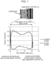
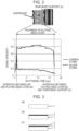
- Figs. 1 and 2 show the results of glow discharge optical emission spectrometry when silver is used as the electrically conductive material (b2).
- the interface between the plating seed layer (B) and the temporary support (A) (the metal plating layer (E) side in the final state) appears at about 16 seconds after the start of sputtering, and a large amount of carbon atoms are present at the interface.
- the functional group included in the dispersant (b1) and the functional group [X] included in the compound (c1) contained in the resin layer (C) described later can easily react with each other to form a chemical bond.
- the interface between the plating seed layer (B) and the temporary support (A) (the metal plating layer (E) side in the final state) is located at about 21 seconds after the start of sputtering at which the signal intensity of silver atoms drops. However, no increase in the amount of carbon atoms is found at the interface.
- the plating seed layer (B) may be a layer provided on the entire surface of the temporary support (A) or may be a layer provided on part of the surface of the temporary support (A).
- An electrically conductive pattern obtained using the plating seed layer (B) may be a pattern in which the plating seed layer (B) is formed on the entire surface of the temporary support (A) or may be a pattern in which the plating seed layer (B) is formed on part of the surface.
- the plating seed layer (B) contains the electrically conductive material (b2) in the range of 80% by mass to 99.9% by mass with respect to the total mass of the plating seed layer (B) and contains the dispersant (b1) in the range of 0.1% by mass to 20% by mass and preferably in the range of 0.1% by mass to 10% by mass.
- the dispersant (b1) containing a basic nitrogen-containing group is preferably a high-molecular weight dispersant, and the high-molecular weight dispersant used is preferably a polyalkylenimine such as polyethyleneimine or polypropyleneimine or a compound prepared by adding polyoxyalkylene to a polyalkylenimine.
- the dispersant used is a high-molecular weight dispersant
- the dispersant in the plating seed layer (B) can be removed more easily than a low-molecular weight dispersant to form a porous layer, and larger pores can be formed.
- pores of the order of nanometers to submicron order can be formed.
- the pores can be easily filled with the metal forming the metal plating layer (E) described later, and the metal in the pores serves as an anchor, so that the adhesion between the plating seed layer (B) and the metal plating layer (E) described later can be significantly improved.
- Examples of the monomer having a phosphate group include 2-((meth)acryloyloxy)ethyl phosphate, 2-((meth)acryloyloxy)propyl phosphate, diphenyl(2-acryloyloxyethyl) phosphate, diphenyl(2-methacryloyloxyethyl) phosphate, and phenyl(2-acryloyloxyethyl) phosphate.
- a functional group [Y] other than the phosphate group for the dispersant (b1) in combination with the phosphate group in order to improve the adhesion between the plating seed layer (B) and the resin layer (C).
- the functional group [Y] include a carboxyl group, an isocyanate group, a blocked isocyanate group, an epoxy group, a hydroxy group, an oxazoline group, an N-methylol group, an N-alkoxymethyl group, an amino group, and an alkoxysilyl group.
- the dispersant (b1) may include two or more of the functional groups.
- Examples of the electrically conductive material (b2) included in the plating seed layer (B) include transition metals and compounds thereof.
- ionic transition metals are preferred.
- Examples of the ionic transition metal include copper, silver, gold, nickel, palladium, platinum, and cobalt.
- silver and copper are preferred because the metal plating layer (E) described later can be easily formed, and silver is used more preferably because the surface resistance of the plating seed layer can be reduced.
- Metals having magnetism such as nickel and cobalt reduce transmission characteristics required for high-frequency transmission. It is therefore preferable to use silver or copper, and it is more preferable to use silver.
- the electrically conductive material (b2) used to form the plating seed layer (B) has a particulate or fibrous shape.
- the electrically conductive material (b2) is particles, it is preferable that the particles are of the order of nanometers.
- the average particle diameter is preferably in the range of 1 to 100 nm and more preferably in the range of 1 to 50 nm because a denser coating film can be obtained and the resistance can be further reduced.
- "Nanotrac UPA-150" manufactured by Microtrac can be used.
- the diameter of the fibers is preferably in the range of 5 to 100 nm and more preferably in the range of 5 to 50 nm because a denser coating film can be obtained and the resistance can be further reduced.
- the length of the fibers is preferably in the range of 0.1 to 100 ⁇ m and more preferably in the range of 0.1 to 30 ⁇ m.
- a dispersant may also be used.
- the dispersant include dodecanethiol, 1-octanethiol, triphenylphosphine, dodecylamine, polyethylene glycol, polyvinylpyrrolidone, polyethyleneimine, polyvinylpyrrolidone; fatty acids such as myristic acid, octanoic acid, and stearic acid; polycyclic hydrocarbon compounds having a carboxyl group such as cholic acid, glycyrrhizic acid, and abietic acid, urethane resins, acrylic resins, and compounds in which a phosphate group is included in a urethane or acrylic resin.
- the amount of the dispersant used to disperse the electrically conductive material (b2) is preferably in the range of 0.01 to 50 parts by mass and more preferably in the range of 0.01 to 10 parts by mass based on 100 parts by mass of the electrically conductive material (b2).
- the solvent used for the fluid may be a water-based solvent or an organic solvent.
- the water-based solvent include distilled water, ion exchanged water, pure water, and ultrapure water.
- organic solvent include alcohol compounds, ether compounds, ester compounds, and ketone compounds.
- Examples of the alcohol compound include methanol, ethanol, n-propanol, isopropyl alcohol, n-butanol, isobutyl alcohol, sec-butanol, tert-butanol, heptanol, hexanol, octanol, nonanol, decanol, undecanol, dodecanol, tridecanol, tetradecanol, pentadecanol, stearyl alcohol, allyl alcohol, cyclohexanol, terpineol, terpineol, dihydroterpineol, ethylene glycol monomethyl ether, ethylene glycol monoethyl ether, ethylene glycol monobutyl ether, diethylene glycol monoethyl ether, diethylene glycol monomethyl ether, diethylene glycol monobutyl ether, tetraethylene glycol monobutyl ether, propylene glycol monomethyl ether
- ethylene glycol diethylene glycol, 1,3-butanediol, isoprene glycol, glycerin, etc. may be optionally used for the fluid.
- the surfactant used may be a commonly-used surfactant, and examples thereof include di-2-ethylhexyl sulfosuccinate, dodecylbenzenesulfonate, alkyl diphenyl ether disulfonate, alkylnaphthalenesulfonate, and hexametaphosphate.
- the leveling agent used may be a commonly-used leveling agent, and examples thereof include silicone-based compounds, acetylenediol-based compounds, and fluorine-based compounds.
- the viscosity modifier used may be a commonly-used thickener, and examples thereof include: acrylic polymers and synthetic rubber latexes that can increase viscosity by adjusting the pH to alkaline; and urethan resins, hydroxyethyl cellulose, carboxymethyl cellulose, methyl cellulose, polyvinyl alcohol, hydrogenated castor oil, amide waxes, polyethylene oxide, metal soaps, and dibenzylidene sorbitol that can increase viscosity by molecular association.
- the antifoaming agent used may be a commonly-used antifoaming agent, and examples thereof include silicone-based antifoaming agents, nonionic surfactants, polyethers, higher alcohols, and polymer-based surfactants.
- the preservative used may be a commonly-used preservative, and examples thereof include isothiazoline-based preservatives, triazine-based preservatives, imidazole-based preservatives, pyridine-based preservatives, azole-based preservatives, and pyrithione-based preservatives.
- the viscosity of the fluid (a value measured at 25°C using a B type viscometer) is preferably in the range of 0.1 to 500,000 mPa ⁇ s and more preferably in the range of 0.2 to 10,000 mPa ⁇ s.
- the viscosity is preferably in the range of 5 to 20 mPa ⁇ s.
- the drying temperature after the application or printing of the fluid containing the dispersant (b1) and the electrically conductive material (b2) is preferably in the range of 50°C to 400°C, more preferably in the range of 80°C to 340°C, preferably in the range of 120°C to 320°C, preferably in the range of 150°C to 300°C, and still more preferably in the range of 180°C to 280°C.
- the adhesion between the plating seed layer (B) and the metal plating layer (E) can be improved.
- the mass of the plating seed layer (B) per unit area is preferably in the range of 1 to 30000 mg/m 2 and preferably in the range of 1 to 5,000 mg/m 2 .
- the plating seed layer (B) is used as a catalyst.
- the thickness of the plating seed layer can be small.
- the mass per unit area is preferably 1 to 5000 mg/m 2 , preferably 10 to 1000 mg/m 2 , preferably 10 to 500 mg/m 2 , and more preferably 50 to 500 mg/m 2 .
- the plating seed layer (B) needs to have electrical conductivity. In this case, the lower the resistance, the better.
- the surface resistance of the plating seed layer (B) is low in order to form uniform electroplating.
- the surface resistance is preferably in the range of 0.1 to 10000 ⁇ / ⁇ , more preferably in the range of 0.15 to 1000 ⁇ / ⁇ , more preferably in the range of 0.15 to 500 ⁇ / ⁇ , more preferably in the range of 0.2 to 100 ⁇ / ⁇ , more preferably in the range of 0.2 to 10 ⁇ / ⁇ , and still more preferably in the range of 0.2 to 5 ⁇ / ⁇ .
- the resin layer (C) is a layer provided for the purpose of increasing the area ratio (transfer ratio) of the plating seed layer (B) successfully transferred to the support (D) described later when the transfer layered body is laminated to the support (D) in the manner described later to thereby increase the adhesion between the plating seed layer (B) and the support (D).
- the resin layer (C) is formed as a coating film (c) prepared by applying a composition (c1-1) containing the compound (c1) having the functional group [X] to the surface of the plating seed layer (B) and drying the composition.
- the functional group [X] included in the compound (c1) present in the coating film (c) reacts with the basic nitrogen atom-containing group or phosphate group in the dispersant (b1) contained in the plating seed layer (B) to form a chemical bond.
- the reaction proceeds at room temperature, and the chemical bond is formed. However, the reaction proceeds more easily under heating, and the formation of the chemical bond is facilitated.
- the adhesion at the interface between the plating seed layer (B) and the resin layer (C) increases. Therefore, the plating seed layer (B) and the resin layer (C) are not easily separated from each other when the transfer layered body is laminated to the support (D) in the manner described later and then the temporary support (A) of the transfer layered body is removed. Moreover, a structure including the resin layer (C) and the plating seed layer (B) stacked on the support (D) described later can have an electrically conductive pattern with adhesion high enough to prevent delamination over time.
- the coating film (c) that can serve as a precursor of the resin layer (C) is formed by applying a composition containing the compound (c1) having the functional group [X] to the surface of the support and, for example, drying the composition.
- the compound (c1) contained in the coating film (c) has the functional group [X] that is reactable with the basic nitrogen atom-containing group or the phosphate group in the dispersant (b1) contained in the plating seed layer (B).
- the amount of the functional groups [X] present with respect to the total amount of the resin layer (C) is preferably in the range of 50 mmol/kg to 10,000 mmol/kg and more preferably in the range of 100 mmol/kg to 8,000 mmol/kg and is still more preferably in the range of 100 mmol/kg to 5,000 mmol/kg because the adhesion can be further improved.
- Examples of the resin layer (C) include urethane resins, acrylic resins, core-shell composite resins including a urethane resin serving as a shell and an acrylic resin serving as a core, epoxy resins, phenoxy resins, imide resins, amide resins, melamine resins, phenolic resins, urea-formaldehyde resins, blocked isocyanate polyvinyl alcohols obtained by allowing polyisocyanate to react with a blocking agent such as phenol, and polyvinylpyrrolidone.
- the core-shell composite resin including a urethane resin serving as a shell and an acrylic resin serving as a core can be obtained, for example, by polymerizing an acrylic monomer in the presence of a urethane resin.
- One of the above resins may be used alone, or a combination of two or more may be used.
- a resin containing an aminotriazine-modified novolac resin is used as the resin forming the resin layer (C).
- the phenolic hydroxy group (functional group [X]) in the aminotriazine novolac resin and the basic nitrogen atom-containing group included in the plating seed layer (B) undergo an acid-base reaction to form an ionic bond, and the adhesion at the interface between the plating seed layer (B) and the resin layer (C) is improved.
- the aminotriazine-modified novolac resin is a novolac resin in which an aminotriazine ring structure and a phenol structure are bonded via a methylene group.
- the aminotriazine-modified novolac resin is obtained, for example, by the co-condensation reaction of an aminotriazine compound such as melamine, benzoguanamine, or acetoguanamine, a phenol compound such as phenol, cresol, butylphenol, bisphenol A, phenylphenol, naphthol, or resorcin, and formaldehyde near a neutral pH in the presence of a weak alkaline catalyst such as an alkylamine or without any catalyst or by the reaction of an alkyl ether of an aminotriazine compound such as methyletherified melamine and any of the above phenol compounds.
- a weak alkaline catalyst such as an alkylamine or without any catalyst
- an alkyl ether of an aminotriazine compound such
- the aminotriazine-modified novolac resin has substantially no methylol group.
- the aminotriazine-modified novolac resin may include molecules including only methylene-linked aminotriazine structures and molecules including only methylene-linked phenol structures that are generated as byproducts during production.
- the aminotriazine-modified novolac resin may contain a small amount of unreacted raw materials.
- the hydroxyl value of the aminotriazine-modified novolac resin is preferably in the range of 50 to 200 mgKOH/g, more preferably in the range of 80 to 180 mgKOH/g, and still more preferably in the range of 100 to 150 mgKOH/g because the adhesion can be further improved.
- One aminotriazine-modified novolac resin may be used alone, or a combination of two or more may be used.
- the epoxy resin examples include a bisphenol A-type epoxy resin, a bisphenol F-type epoxy resin, a biphenyl-type epoxy resin, a cresol novolac-type epoxy resin, a phenol novolac-type epoxy resin, a bisphenol A novolac-type epoxy resin, an alcohol ether-type epoxy resin, a tetrabromobisphenol A-type epoxy resin, a naphthalene-type epoxy resin, a phosphorus-containing epoxy compound having a structure derived from a 9,10-dihydro-9-oxa-10-phosphaphenanthrene-10-oxide derivative, an epoxy resin having a structure derived from a dicyclopentadiene derivative, and epoxidized products of fats and oils such as epoxidized soybean oil.
- One of these epoxy resins may be used alone, or a combination of two or more may be used.
- a curing accelerator may also be used.
- the curing accelerator include an amine compound having a primary, secondary, or tertiary amino group.
- the amine compound used may be any of aliphatic, alicyclic, and aromatic amine compounds.
- Other examples of the curing accelerator that can be used include mercaptans, acid anhydrides, acid boron fluoride, borates, organic acid hydrazides, Lewis acids, organometallic compounds, onium salts, and cationic compounds.
- the resin layer (C) has the function of improving the adhesion between the support (D) and the plating seed layer (B) as described later.
- the phenoxy resin used has a weight average molecular weight in the range of 10,000 to 100,000.
- the adhesion between the support (D) and the metal plating layer (E) can be improved.
- the high-molecular weight phenoxy resin is used, deterioration such as decomposition of the polymer due to heat during a long-term heat resistance test can be prevented. Therefore, even after the long-term heat resistance test, the adhesion to the metal plating layer (E) can be maintained.
- phenoxy resins having skeleton structures such as a novolac structure, an anthracene structure, a fluorene structure, a dicyclopentadiene structure, a norbornene structure, a naphthalene structure, a biphenyl structure, and an adamantane structure.
- One of these phenoxy resins may be used alone, or a mixture of two or more may be used.
- phenoxy resins having a bisphenol structure are preferred, and a bisphenol A skeleton, a bisphenol F skeleton, and a bisphenol S skeleton are more preferred.
- the phenoxy resin may have any functional group such as a phenolic hydroxy group or an epoxy group at each end.
- the weight average molecular weight of the phenoxy resin used is preferably in the range of 10,000 to 100,000.
- the molecular weight is 10,000 or more, the adhesion of the plating after the long-term heat resistance test is high.
- the molecular weight is 100,000 or less, the solubility in an organic solvent is improved, and the coating solution used to form the resin layer (C) can have an appropriate viscosity, so that good handleability is achieved.
- the weight average molecular weight of the phenoxy resin is preferably 20,000 to 80,000 and more preferably 22,000 to 50,000.
- the weight average molecular weight of the phenoxy resin can be adjusted by changing the molar ratio of the epoxy resin to the phenolic resin and the reaction time in the reaction described above.
- the weight average molecular weight used is a standard polystyrene-equivalent value measured by gel permeation chromatography (GPC) described later.
- GPC gel permeation chromatography
- a high performance GPC HEC-8420GPC manufactured by TOSOH Corporation
- TSKgel G5000HxL/G4000HxL/G3000HxL/G2000HxL manufactured by TOSOH Corporation
- the eluent used was tetrahydrofuran, and an RI detector was used for the measurement.
- the phenoxy resin generally means a high-molecular weight epoxy resin.
- the term "epoxy resin” means a resin having a weight average molecular weight of less than 10,000 and is distinguished from the phenoxy resin described above.
- the epoxy resin examples include a bisphenol A-type epoxy resin, a bisphenol F-type epoxy resin, a biphenyl-type epoxy resin, a cresol novolac-type epoxy resin, a phenol novolac-type epoxy resin, a bisphenol A novolac-type epoxy resin, an alcohol ether-type epoxy resin, a tetrabromobisphenol A-type epoxy resin, a naphthalene-type epoxy resin, a phosphorus-containing epoxy compound having a structure derived from a 9,10-dihydro-9-oxa-10-phosphaphenanthrene-10-oxide derivative, an epoxy resin having a structure derived from a dicyclopentadiene derivative, and epoxidized products of fats and oils such as epoxidized soybean oil.
- One of these epoxy resins may be used alone, or a combination of two or more may be used.
- the epoxy resin used in combination with the phenoxy resin is preferably an aromatic epoxy resin such as a bisphenol A-type epoxy resin, a bisphenol F-type epoxy resin, a biphenyl-type epoxy resin, a cresol novolac-type epoxy resin, a phenol novolac-type epoxy resin, or a bisphenol A novolac-type epoxy resin, more preferably a liquid epoxy resin, and particularly preferably a bisphenol A-type epoxy resin because the adhesion to the metal plating layer (E) described later can be further improved.
- aromatic epoxy resin such as a bisphenol A-type epoxy resin, a bisphenol F-type epoxy resin, a biphenyl-type epoxy resin, a cresol novolac-type epoxy resin, a phenol novolac-type epoxy resin, or a bisphenol A novolac-type epoxy resin, more preferably a liquid epoxy resin, and particularly preferably a bisphenol A-type epoxy resin because the adhesion to the metal plating layer (E) described later can be further improved.
- the phenoxy resin when used for the resin layer (C), an epoxy group at a terminal end of the phenoxy resin reacts with a basic nitrogen atom-containing group included in the plating seed layer (B), so that the adhesion at the interface between the plating seed layer (B) and the resin layer (C) is improved.
- the phenoxy resin may be used in combination with another resin.
- the number of resin layers (C) may be one or may be two or more.
- the layer close to the plating seed layer can improve the adhesion to the plating seed layer (B), and the resin layer (C) close to the support (D) described later in the final state can improve the adhesion to the support (D).
- the first resin layer (C) close to the plating seed layer (C) is a layer close to the plating seed layer (B) and the metal plating layer (E) described later and is a portion close to copper traces after the formation of an electrically conductive pattern. Therefore, the resin layer (C) may be formed by selecting a suitable resin composition for the purpose of improving insulation reliability.
- the coating material for the resin layer (C) is applied to the surface of the plating seed layer (B) formed on the surface of the temporary support (A), and it is preferable to add an organic solvent to the coating material in order to obtain a viscosity suitable for application.
- organic solvent include toluene, ethyl acetate, methyl ethyl ketone, methyl isobutyl ketone, cyclohexanone, isopropyl alcohol, diacetone alcohol, ethylene glycol, and toluene.
- One of these solvent may be used alone, or a combination of two or more may be used.
- the drying temperature for the resin layer (C) is preferably in the range of 50°C to 400°C, more preferably in the range of 80°C to 340°C, preferably in the range of 120°C to 280°C, and still more preferably in the range of 150°C to 200°C.
- the surface of the resin layer (C) may be subjected to surface treatment in advance using plasma discharge treatment such as corona discharge treatment, a dry treatment method such as a UV treatment method, or a wet treatment method using water, an acidic or alkaline chemical, or an organic solvent because, in a laminate prepared by laminating a surface of the resin layer (C) of the transfer layered body described later to the support (D) and removing the temporary support (A), the adhesion between the resin layer (C) and the support (D) can be further improved.
- plasma discharge treatment such as corona discharge treatment
- a dry treatment method such as a UV treatment method
- the support (D) is used as a substrate for forming an electrically conductive pattern, and a different support (D) must be used depending on the intended application such as a printed wiring board, a flexible printed wiring board, a rigid printed wiring board, a package substrate, a ceramic substrate, a glass substrate, a silicon wafer substrate, a metal substrate, an electromagnetic shielding film, or a molded interconnect device.
- Examples of the material of the support (D) include polyimide resins, modified polyimide (MPI) resins, polyamide-imide resins, polyamide resins, polyethylene terephthalate resins, polybutylene terephthalate resins, polyethylene naphthalate resins, polycarbonate resins, acrylonitrile-butadiene-styrene (ABS) resins, polyarylate resins, polyacetal resins, acrylic resins such as polymethyl (meth)acrylate, polyvinylidene fluoride resins, polytetrafluoroethylene resins, polyvinyl chloride resins, polyvinylidene chloride resins, vinyl chloride resins obtained by graft-copolymerizing acrylic resins, polyvinyl alcohol resins, polyethylene resins, polypropylene resins, urethane resins, cycloolefin resins, polystyrene, liquid crystal polymers (LCPs), polyether ether ketone (PEE
- the support (D) may be in any form such as a flat flexible form, a rigid form, or a rigid flexible form. More specifically, the support (D) used may be a commercial material formed into a film, a sheet, or a plate or may be a material formed using a solution, melt, or dispersion of any of the above resins into a flat shape.
- the support (D) may be a substrate prepared by disposing any of the above resin materials on an electrically conductive material such as a metal or may be a substrate prepared by stacking any of the above resin materials on a printed wiring board having a circuit pattern formed thereon. Any stacking method may be used.
- the support (D) When the support (D) is a semi-cured support such as a prepreg, the support (D) may be laminated to a printed wiring board having a circuit pattern under heat and pressure. When the support (D) is a fully cured support, an adhesive sheet such as a bonding sheet is used to stack the support (D).
- the rigid wiring board used may be, for example, a glass fiber-epoxy resin composite substrate (a glass-epoxy resin, FR-4, FR-5), a paper-epoxy resin composite substrate (FR-3), a glass nonwoven fabric-epoxy resin composite substrate (CEM-3), a paper-glass nonwoven fabric-epoxy resin composite substrate (CEM-1), a paper-phenolic resin composite substrate (a paper-phenolic resin, FR-1, FR-2), a glass fiber-PPE resin composite substrate (e.g., MEGTRON 6 manufactured by Panasonic Corporation), a bismaleimide-triazine resin (BT resin), a silica-epoxy resin composite substrate (e.g., a build-up film manufactured by Ajinomoto Co., Inc.), a polyimide, a liquid crystal polymer, polyether ether ketone, polyphenylene sulfide, polystyrene, polycarbonate, a polyester resin, polyimide, a liquid crystal polymer, polyether
- Examples of the method for smoothing the support (D) include a method in which the surface of the support (D) is physically smoothed and a method in which the surface of the support (D) is chemically smoothed.
- Examples of the physical smoothing method include calendering in which the support (D) is caused to pass between smooth rolls to smoothen the surface, cutting, grinding, abrasive polishing, discharge processing, laser processing, and water jet processing.
- Examples of the chemical smoothing method include electropolishing and etching.
- the surface roughness of the smoothing treatment substrate is small, and the surface roughness (maximum height Sz) measured using a laser microscope is preferably in the range of 0.001 to 30 ⁇ m, preferably in the range of 0.01 to 20 ⁇ m, and more preferably in the range of 0.05 to 10 ⁇ m.
- the surface roughness (maximum height Sz) is measured using an evaluation method described in ISO 25178 and represents the distance from the highest point on the surface to the lowest point.
- a surface of the resin layer (C) of the transfer layered body described later is laminated to the support (D), and then the temporary support (A) of the transfer layered body is removed to thereby obtain a laminate in which the resin layer (C) and the plating seed layer (B) are formed on the surface of the support (D).
- fine irregularities that do not impair smoothness may be formed on the surface of the support (D) as needed, or the support (D) may be subjected to surface treatment in order to introduce functional groups such as hydroxyl groups, carbonyl group, or carboxyl groups.
- the surface treatment method include plasma discharge treatment such as corona discharge treatment, dry treatment such as UV treatment, and wet treatment using water, an aqueous solution of an acid, an alkali, etc., an organic solvent, etc.
- the transferring method used may include laminating a surface of the resin layer (C) of the transfer layered body to the support (D) using heat and pressure.
- Examples of the method that can be used include, but not particularly limited to, a thermal lamination method, a solventless lamination method, an extrusion lamination method, a wet lamination method, a heat roll transfer method, an in-mold transfer method, a pressing method, a vacuum pressing method, and a water pressure transfer method.
- the support (D) is a roll film formed of a flexible material
- a thermal lamination method is more preferred because the treatment is particularly simple.
- the support (D) is formed of a rigid material
- the support (D) in the form of a flat sheet is generally subjected to thermocompression bonding, and it is preferable to use a pressing method or a vacuum pressing method.
- the metal plating layer (E) or the patterned resist described later is formed on the surface of the plating seed layer (B). It is therefore preferable to perform cleaning treatment for cleaning out components that reduce the adhesion of the metal plating layer (E) or the patterned resist described later to the plating seed layer (B).
- the temporary support (A) is, for example, a resin film
- the components that reduce the adhesion include an oligomer component that is present in the film and bleeds to the surface of the film.
- the components when the release layer is formed on the temporary support (A) include a component of the release agent partially having migrated to the plating seed layer (C).
- the electroless plating method is a method in which, for example, an electroless plating solution is brought into contact with the metal forming the plating seed layer (B) to allow a metal such as copper contained in the electroless plating solution to precipitate to thereby form an electroless plating layer (coating) formed of a metal coating.
- the electroplating method is a method for forming an electroplating layer (metal coating). For example, an electroplating solution is brought into contact with the metal forming the plating seed layer (B) or the surface of an electroless plating layer (coating) formed by the electroless plating, and an electric current is applied while this state is maintained. Then a metal such as copper contained in the electroplating solution is precipitated on the electrically conductive material (b2) forming the plating seed layer (B) serving as a cathode or the electroless plating layer (coating) formed by the electroless plating to thereby form the electroplating layer (metal coating).
- an electroplating solution is brought into contact with the metal forming the plating seed layer (B) or the surface of an electroless plating layer (coating) formed by the electroless plating, and an electric current is applied while this state is maintained. Then a metal such as copper contained in the electroplating solution is precipitated on the electrically conductive material (b2) forming the plating seed layer (B
- the electroplating solution examples include a solution containing a sulfide of a metal such as copper, nickel, chromium, cobalt, or tin, sulfuric acid, and a water-based solvent.
- a solution containing copper sulfate, sulfuric acid, and a water-based solvent examples include a solution containing copper sulfate, sulfuric acid, and a water-based solvent.
- the thickness of the metal plating layer (E) is preferably in the range of 0.01 ⁇ m or more and 100 ⁇ m or less and more preferably in the range of 0.5 ⁇ m or more and 50 ⁇ m or less.
- the thickness of the metal plating layer (E) can be adjusted by controlling the treatment time, the current density, the amount of an additive used for plating, etc. in the plating treatment step of forming the metal plating layer (E).
- Examples of a method for patterning the metal plating layer (E) include: photolithography-etching methods such as a subtractive process and a semi-additive process; and a method in which a print pattern on the metal particle layer (C) is plated.
- the subtractive process is a method for forming a desired pattern by forming an etching resist layer having a shape corresponding to the desired pattern shape on the metal plating layer (E) included in the laminate of the invention produced in advance and then performing developing treatment using a chemical to dissolve and remove the metal plating layer (E) and the plating seed layer (B) in the portions with the resist removed therefrom.
- the chemical used can be a chemical containing copper chloride, iron chloride, etc.
- At least one selected from the group consisting of palladium, an electrically conductive polymer, carbon, and an electrically conductive paste is applied to the surface (wall surface) of the through or blind hole to impart electrical conductivity to the through or blind hole.
- the temporary support (A) of the transfer layered body is removed.
- the plating seed layer (B) is subjected to surface treatment, and a plating resist layer having a shape corresponding to the desired pattern is formed on the treated surface.
- the metal plating layer (E) is formed by an electroplating method, and the plating resist layer and the plating seed layer (B) in contact therewith are dissolved and removed using a chemical etc. to thereby form the desired pattern.
- the plating seed layer (B) is silver, it is preferable that a chemical described later that selectively etches silver is used for the etching.
- electrical continuity can be provided between the front and back sides as follows.
- the temporary support (A) is not removed after the surface of the resin layer (C) of the transfer layered body is laminated to the support (D), so that the temporary support (A) can play a role in protecting the surface of the plating seed layer as described later. More specifically, after the transfer layered body is laminated to the support (D), a through hole or a blind hole is formed from the front side of the temporary support (A) using a drill or a laser.
- the temporary support (A) of the transfer layered body is removed.
- the plating seed layer (B) is subjected to surface treatment, and a plating resist layer having a shape corresponding to the desired pattern is formed on the treated surface.
- the metal plating layer (E) is formed by an electroplating method, and the plating resist layer and the plating seed layer (B) in contact therewith are dissolved and removed using a chemical etc. to thereby form the desired pattern.
- the plating seed layer (B) is silver, it is preferable that a chemical described later that selectively etches silver is used for the etching.
- Electrical continuity can also be provided between the front and back sides by filling the through hole or the blind hole with an electrically conductive paste.
- a through hole or a blind hole is formed from the front side of the temporary support (A) using a drill or a laser. Then the temporary support (A) of the transfer layered body is removed.
- the plating seed layer (B) is subjected to surface treatment, and a plating resist layer having a shape corresponding to the desired pattern is formed on the treated surface.
- the metal plating layer (E) is formed by an electroplating method. Then the plating resist layer and the plating seed layer (B) in contact therewith are dissolved and removed using a chemical etc. to thereby form the desired pattern.
- the through hole or the blind hole is filled with an electrically conductive paste by, for example, a screen printing method, and the electrically conductive paste is heated to provide electrical continuity between the front and back sides.
- the temporary support (A) may remain stacked on the plating seed layer (B).
- organic and inorganic dust (smears) generated in the step of forming a through hole extending between both sides described later in the printed wiring board production method of the invention is prevented from adhering to the surface of the plating seed layer (B).
- palladium, an electrically conductive polymer, carbon, or an electrically conductive paste is prevented from adhering to the electrically conductive plating seed layer (B), and the plating seed layer (B) is thereby protected.
- the hole diameter (diameter) of the hole formed by the hole forming process is preferably in the range of 0.01 to 1 mm, more preferably in the range of 0.02 to 0.5 mm, and still more preferably in the range of 0.03 to 0.1 mm.
- Organic and inorganic dust (smears) generated during the hole forming process may cause breakage of the electrical connection between both sides, faulty plating deposited in the metal plating step for forming the metal plating layer (E), a reduction in adhesion of the plating, and deterioration of the appearance of the plating. It is therefore preferable to remove the dust (perform desmearing).
- the desmearing method include: dry treatment such as plasma treatment and reverse sputtering treatment; and wet treatment such as cleaning treatment using an aqueous solution of an oxidizer such as potassium permanganate, cleaning treatment using an aqueous solution of an alkali or an acid, and cleaning treatment using an organic solvent.
- palladium, an electrically conductive polymer, an electrically conductive paste, or carbon is applied to the surface of the thorough or blind hole to impart electrical conductivity to the surface of the through or blind hole.
- Electrical conductivity can be imparted to the surface of the through hole with reference to, for example, a method described in " Direct plating” by TOYONAGA Minoru, Circuit Technology, vol. 8, No. 1 (1993) pp. 47-59 .
- one of four systems (1) a palladium-tin colloidal system, (2) a tin free-palladium system, (3) an electrically conductive polymer system, and (4) a graphite system described in the above reference may be used.
- An electrically conductive paste may be used to impart electrical conductivity to the surface of the through hole.
- the surface of the laminate with the through hole formed therein is subjected to cleaner-conditioner treatment. Then the tin-palladium colloid is caused to adsorb on the surface, and the surface is subjected to accelerator treatment to remove tin.
- a method in which palladium is converted to palladium sulfide may be also used to increase the electrical conductivity.
- the surface of the laminate having the through hole formed therein is treated with a carbon black suspension solution to cause carbon to adsorb onto the entire surface of the substrate.
- a carbon black suspension solution to cause carbon to adsorb onto the entire surface of the substrate.
- the electrically conductive paste is applied to the surface of the laminate having the through hole formed therein to thereby impart electrical conductivity to the wall of the through hole and is used as a seed layer for electroplating performed in the subsequent step.
- the surface of the laminate with the through hole formed therein is treated by a dry plating method.
- a dry plating method for example, a method in which a film is formed on the surface of the through hole by a vacuum deposition method, an ion plating method, or a sputtering method to impart electrical conductivity can be preferably used.
- a dry plating method no particular limitation is imposed on the metal used for imparting electrical conductivity so long as electrical conductivity can be imparted to the surface of the through hole and connection between both sides by the copper electroplating in the subsequent step is not impaired, and various metals and metal oxides can be used.
- the temporary support layer (A) may be removed mechanically, or any commercial removal apparatus may be used.
- the temporary support (A) can be removed by immersing it in an alkaline solution.
- a removing solution for a patterned resist described later can be appropriately used as the alkaline solution used for removal, and the removing conditions for the patterned resist can be appropriately used.
- a patterned resist for a circuit pattern is formed on the exposed plating seed layer (B).
- Examples of the commercial dry film include: the "PHOTEC” series manufactured by Hitachi Chemical Company, Ltd.; the “ALPHO” series manufactured by Nikko-Materials Co., Ltd.; the "SUNFORT” series manufactured by Asahi Kasei Corporation; and the "RISTON” series manufactured by DuPont.
- connection via the copper plating in the through hole in the laminate can be achieved, and at the same time an electrically conductive pattern can be formed.
- the annealing temperature may be appropriately selected within the temperature range of 40 to 300°C according to the heat resistance of the substrate used or the intended use purpose.
- the annealing temperature is preferably in the range of 40 to 250°C and is more preferably in the range of 40 to 200°C for the purpose of preventing oxidative deterioration of the plating film.
- the annealing time may be 10 minutes to 10 days when the annealing temperature is in the range of 40 to 200°C and may be 5 minutes to 10 hours when the annealing is performed at a temperature exceeding 200°C.
- an anticorrosive may be optionally applied to the surface of the plating film.
- the patterned resist is removed.
- the patterned resist formed using the photosensitive resist is removed, and the plating seed layer (B) in non-pattern-formed portions is removed using an etching solution.
- the patterned resist may be removed under the recommended conditions described in the brochure or instructions of the photosensitive resist used.
- the resist remover used to remove the patterned resist may be a commercial resist remover or a 1.5 to 3% by mass aqueous sodium hydroxide or potassium hydroxide solution set to 45 to 60°C.
- the resist can be removed by immersing the substrate with the pattern formed thereon in the remover or spraying the remover using a sprayer etc.
- carboxylic acids may be used alone, or a combination of two or more may be used. It is preferable that, among these carboxylic acids, acetic acid or citric acid is mainly used because the etching solution can be easily produced and can be easily handled.
- polyalkylene glycol examples include water-soluble polymers such as polyethylene glycol, polypropylene glycol, and a polyoxyethylene polyoxypropylene block copolymer. Of these, polyethylene glycol is preferred.
- the number average molecular weight of the polyalkylene glycol is preferably in the range of 200 to 20,000.
- An additive such as a sodium, potassium, or ammonium salt of an organic acid may be optionally added to the etching solution in order to reduce the change in pH .
- the etching solution with the amounts of all the components adjusted to the desired composition values may be supplied to the etching apparatus.
- the components of the etching solution may be independently supplied to the etching apparatus and mixed in the apparatus such that the etching solution has the desired composition.
- a cleaning operation other than cleaning with water may be performed for the purpose of preventing the silver component dissolved in the etching solution from adhering to and remaining on the printed wiring board.
- a cleaning solution that can dissolve silver oxide, silver sulfide, and silver chloride but dissolves almost no silver is used for the cleaning operation.
- the cleaning chemical used is preferably an aqueous solution containing a thiosulfate or a tris(3-hydroxyalkyl)phosphine or an aqueous solution containing a mercapto carboxylic acid or a salt thereof.
- the concentration of the alkaline permanganic acid solution may be appropriately selected as needed. It is preferable to use an alkaline permanganic acid solution obtained by dissolving 0.1 to 10 parts by mass of potassium permanganate or sodium permanganate in 100 parts by mass of a 0.1 to 10% by mass aqueous solution of potassium hydroxide or sodium hydroxide. From the viewpoint of cleaning efficiency, it is more preferable to use an alkaline permanganic acid solution obtained by dissolving 1 to 6 parts by mass of potassium permanganate or sodium permanganate in 100 parts by mass of a 1 to 6% by mass aqueous solution of potassium hydroxide or sodium hydroxide.
- the cleaned printed wiring board is treated with a liquid having a neutralization-reduction action.
- the liquid having the neutralization-reduction action include 0.5 to 15% by mass dilute sulfuric acid and an aqueous solution containing an organic acid.
- the organic acid include formic acid, acetic acid, oxalic acid, citric acid, ascorbic acid, and methionine.
- the laminate of the invention may be used to obtain a printed wiring board. If necessary, the printed wiring board obtained may be appropriately subjected to nickel/gold plating, nickel/palladium/gold plating, or palladium/gold plating for the purpose of depositing a cover lay film on the circuit pattern or of forming a solder resist layer, or as final surface treatment of the circuit pattern.
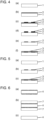
- Fig. 4 shows a method for producing a transfer layered body.
- the transfer layered body is obtained by forming a plating seed layer (B) on a surface of a temporary support (A), forming an electrically conductive pattern using a patterned resist by etching, removing the patterned resist, and then forming a resin (C) over the entire surface of the temporary support (A).
- Fig. 5 shows a method for producing a transfer layered body.
- the transfer layered body is obtained by forming a pattered plating seed layer (B) on a surface of a temporary support (A) using a printing method and then forming a resin (C) over the entire surface of the temporary support (A).
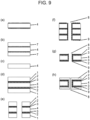
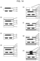
- Fig. 9 shows a method for producing electrically conductive patterns using transfer layered bodies obtained in the manner shown in Fig. 3 , and electrical continuity is provided between the front and back sides of the support (D) using a through hole.
- transfer layered bodies each having a patterned plating seed layer (B) formed thereon and obtained in the manner shown in Fig. 4 or 5 may also be used.
- the transfer layered bodies are laminated to both sides of the support (D).
- a transfer layered body may be laminated to only one side, and another electrically conductive pattern such as a copper foil may be laminated to the other side.
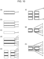
- Fig. 10 shows a method for producing electrically conductive patterns using transfer layered bodies obtained in the manner shown in Fig. 3 , and electrical continuity is provided between the front and back sides of a support (D) via a through hole.
- an irregular support (D) is laminated with a smooth metal foil or a smooth heat resistant film using a hot press etc. such that its smooth surface faces the support (D), and the laminated metal foil or heat resistant film is removed to smoothen the support (D).
- the transfer layered bodies each having a plating seed layer (B) and a resin layer (C) formed over the entire surface of a temporary support (A) are laminated to the support (D) such that the surfaces of the transfer layered bodies that are formed by the resin layers (C) face the smoothed surfaces of the support (D).
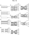
- Fig. 11 shows a method for producing electrically conductive patterns using transfer layered bodies obtained in the manner shown in Fig. 3 , and electrical continuity is provided between the front and back sides of a support (D) via a through hole.
- an irregular support (D) is laminated with a smooth metal foil or a smooth heat resistant film using a hot press etc. such that its smooth surface faces the support (D), and the laminated metal foil or heat resistant film is removed to smoothen the support (D).
- the transfer layered bodies each having a plating seed layer (B) and a resin layer (C) formed over the entire surface of a temporary support (A) are laminated to the support (D) such that the surfaces of the transfer layered bodies that are formed by the resin layers (C) face the smoothed surfaces of the support (D).
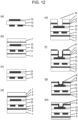
- a through hole passing through the temporary supports (A) of the transfer layered bodies on both sides is formed.
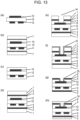
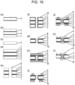
- a support (D) and a smooth metal foil or heat resistant film are sequentially stacked on at least one side of the substrate with the electrically conductive patterns formed thereon and are laminated together by thermocompression bonding, and the metal foil or heat resistant film is removed to smoothen the support (D).
- the transfer layered bodies each having a plating seed layer (B) and a resin layer (C) formed on the entire surface of a temporary support (A) are laminated to the surfaces of the supports (D) such that the surfaces of the transfer layered bodies that are formed by the resin layers (C) face the smoothened surfaces of the supports (D).
- a blind hole extending from the temporary support (A) of one of the transfer layered bodies to one of the electrically conductive patterns on the substrate is formed.
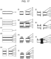
- palladium, an electrically conductive polymer, an electrically conductive paste, or carbon is applied to the one of the transfer layered bodies and the surface of the blind hole to impart electrical conductivity to the surface of the blind hole.
- the temporary supports (A) are removed, and a metal plating layer (E) is formed on the plating seed layers (B) and in the blind hole.
- the supports (D) are subjected to the smoothing treatment. However, when the surfaces of the supports (D) are sufficiently smooth, it is not always necessary to perform the smoothing treatment. In the example in Fig.
- the transfer layered bodies obtained in the manner shown in Fig. 3 are used.
- transfer layered bodies each having a patterned plating seed layer (B) formed thereon and obtained in the manner shown in Fig. 4 or 5 may be used.
- the supports (D) are laminated to both sides of the substrate with the electrically conductive patterns formed thereon, and the transfer layered bodies are further laminated thereto.
- a support (D) and a transfer layered body may be laminated only to one side, and a support (D) and another electrically conductive pattern such as a copper foil may be laminated to the other side.
- a support (D) and a smooth metal foil or heat resistant film are sequentially stacked on at least one side of the substrate with the electrically conductive patterns formed thereon and are laminated together by thermocompression bonding, and the metal foil or heat resistant film is removed to smoothen the support (D).
- the transfer layered bodies each having a plating seed layer (B) and a resin layer (C) formed on the entire surface of a temporary support (A) are laminated to the surfaces of the support (D) such that the surfaces of the transfer layered bodies that are formed by the resin layers (C) face the smoothened surfaces of the supports (D).
- a support (D) and a smooth metal foil or heat resistant film are sequentially stacked on at least one side of the substrate with the electrically conductive patterns formed thereon and are laminated together by thermocompression bonding, and the metal foil or heat resistant film is removed to smoothen the support (D).
- the transfer layered bodies each having a plating seed layer (B) and a resin layer (C) formed on the entire surface of a temporary support (A) are laminated to the surfaces of the support (D) such that the surfaces of the transfer layered bodies that are formed by the resin layers (C) face the smoothened surfaces of the supports (D).
- a blind hole extending from the temporary support (A) of one of the transfer layered bodies to one of the electrically conductive patterns on the substrate is formed.
- the temporary supports (A) are removed, and a metal plating layer (E) is formed on the surfaces of the plating seed layers (B).
- the blind hole is filled with an electrically conductive paste to impart electrical conductivity to the blind hole.
- the supports (D) are subjected to the smoothing treatment. However, when the surfaces of the supports (D) are sufficiently smooth, it is not always necessary to perform the smoothing treatment.
- the transfer layered bodies obtained in the manner shown in Fig. 3 are used.
- an irregular support (D) is laminated with a smooth metal foil or a smooth heat resistant film using a hot press etc. such that its smooth surface faces the support (D), and the laminated metal foil or heat resistant film is removed to smoothen the support (D).
- the transfer layered bodies each having a plating seed layer (B) and a resin layer (C) formed over the entire surface of a temporary support (A) are laminated to the support (D) such that the surfaces of the transfer layered bodies that are formed by the resin layers (C) face the smoothed surfaces of the support (D).
- a through hole passing through the temporary supports (A) of the transfer layered bodies on both sides is formed.
- Fig. 17 shows a method for producing electrically conductive patterns by a semi-additive process using transfer layered bodies obtained in the manner shown in Fig. 3 , and electrical continuity is provided between the front and back sides of a support (D) via a through hole.
- an irregular support (D) is laminated with a smooth metal foil or a smooth heat resistant film using a hot press etc. such that its smooth surface faces the support (D), and the laminated metal foil or heat resistant film is removed to smoothen the support (D).
- the transfer layered bodies each having a plating seed layer (B) and a resin layer (C) formed over the entire surface of a temporary support (A) are laminated to the support (D) such that the surfaces of the transfer layered bodies that are formed by the resin layers (C) face the smoothed surfaces of the support (D).
- a through hole passing through the temporary supports (A) of the transfer layered bodies on both sides is formed.
- Fig. 18 shows a method for producing electrically conductive patterns by a semi-additive process using transfer layered bodies obtained in the manner shown in Fig. 3 , and electrical continuity is provided between the front and back sides of a support (D) via a through hole.
- Fig. 19 shows a method for producing electrically conductive patterns by a semi-additive process using transfer layered bodies obtained in the manner shown in Fig. 3 .
- supports (D) are laminated to a substrate having electrically conductive patterns formed thereon, and the surfaces of the supports (D) are subjected to smoothing treatment. Electrical continuity is provided between the surface of one of the supports (D) and one of the electrically conductive patterns on the substrate via a blind hole.
- a support (D) and a smooth metal foil or heat resistant film are sequentially stacked on at least one side of the substrate with the electrically conductive patterns formed thereon and are laminated together by thermocompression bonding, and the metal foil or heat resistant film is removed to smoothen the support (D).
- the transfer layered bodies each having a plating seed layer (B) and a resin layer (C) formed on the entire surface of a temporary support (A) are laminated to the surfaces of the support (D) such that the surfaces of the transfer layered bodies that are formed by the resin layers (C) face the smoothened surfaces of the supports (D).
- a blind hole extending from the temporary support (A) of one of the transfer layered bodies to one of the electrically conductive patterns on the substrate is formed.
- palladium, an electrically conductive polymer, carbon, or an electrically conductive paste is applied to the one of the transfer layered bodies and the surface of the blind hole to impart electrical conductivity to the surface of the blind hole.
- the temporary supports (A) are removed.
- a patterned resist is formed on the surfaces of the plating seed layers (B), and a metal plating layer (E) is formed on the plating seed layers (B) and in the blind hole.
- Fig. 20 shows a method for producing electrically conductive patterns by a semi-additive process using transfer layered bodies obtained in the manner shown in Fig. 3 .
- supports (D) are laminated to a substrate having electrically conductive patterns formed thereon, and the surfaces of the supports (D) are subjected to smoothing treatment. Electrical continuity is provided between the surface of one of the supports (D) and one of the electrically conductive patterns on the substrate via a blind hole.
- a support (D) and a smooth metal foil or heat resistant film are sequentially stacked on at least one side of the substrate with the electrically conductive patterns formed thereon and are laminated together by thermocompression bonding, and the metal foil or heat resistant film is removed to smoothen the surface of the support (D).
- the transfer layered bodies each having a plating seed layer (B) and a resin layer (C) formed on the entire surface of a temporary support (A) are laminated to the surfaces of the supports (D) such that the surfaces of the transfer layered bodies that are formed by the resin layers (C) face the smoothened surfaces of the supports (D).
- a support (D) and a smooth metal foil or heat resistant film are sequentially stacked on at least one side of the substrate with the electrically conductive patterns formed thereon and are laminated together by thermocompression bonding, and the metal foil or heat resistant film is removed to smoothen the support (D).
- the transfer layered bodies each having a plating seed layer (B) and a resin layer (C) formed on the entire surface of a temporary support (A) are laminated to the surfaces of the supports (D) such that the surfaces of the transfer layered bodies that are formed by the resin layers (C) face the smoothened surfaces of the supports (D).
- a blind hole extending from the temporary support (A) of one of the transfer layered bodies to one of the electrically conductive patterns on the substrate is formed.
- the temporary supports (A) are removed, and a patterned resist is formed on the surfaces of the plating seed layers (B).
- a metal plating layer (E) is formed on the plating seed layers (B).
- the patterned resist is removed, and an etching solution is used to remove the plating seed layers (B) from portions other than portions in which the metal plating layer (E) serving as electrically conductive patterns is formed.
- the blind hole is filled with an electrically conductive paste to impart electrical conductivity to the blind hole.
- the supports (D) are subjected to the smoothing treatment.
- substrates for high-density high-performance printed wiring boards having various shapes and sizes and these printed wiring boards can be preferably provided at low cost, and the industrial applicability in the field of printed wiring boards is high.
- the powder of the obtained silver particles having a basic nitrogen atom-containing group was dispersed in a solvent mixture of 45 parts by mass of ethanol and 55 parts by mass of ion exchanged water to prepare a 5% by mass coating solution (1) for forming a plating seed layer (B).
- the ratio of the dispersant in the obtained silver particles was computed using ashes obtained by heating the silver particles at 500°C for 1 hour in an electric furnace and was found to be 5% by mass with respect to 100% by mass of the solid silver.
- a reaction vessel equipped with a stirrer, a reflux condenser tube, a nitrogen introduction tube, a thermometer, a dropping funnel for dropwise addition of a monomer, and a dropping funnel for dropwise addition of a polymer was charged with 140 parts by mass of deionized water and 100 parts by mass of the above-obtained water dispersion of the urethane resin, and the mixture was heated to 80°C while nitrogen was blown into the mixture.
- the coating solution (1) used to form a resin layer (C) and obtained in Preparation Example 3 was applied using a desktop compact coater ("K Printing Proofer” manufactured by RK Print Coat Instruments) and dried at 180°C for 3 minutes such that the dry thickness of a layer corresponding to the resin layer (C) was 0.3 ⁇ m.
- the plating seed layer (B) and the resin layer (C) were thereby formed on the surface of the release film corresponding to the temporary support (A), and a transfer layered body (1) was obtained. Cuts were made on the surface with the resin layer (C) formed thereon using a cutter to form 100 squares with a side of 1 mm, and a cross-cut peel test using an adhesive tape was performed.
- the plating seed layer (B) on the copper foil was analyzed using a glow discharge optical emission spectrometer.
- the signal intensity of carbon atoms present at the interface between air and the plating seed layer (B) was 0.5, and the signal intensity of carbon atoms present at the interface between the plating seed layer (B) and the release film was 0.1.
- the coating solution (1) used to form a resin layer (C) and obtained in Preparation Example 3 was applied using a desktop compact coater ("K Printing Proofer” manufactured by RK Print Coat Instruments) and dried at 180°C for 3 minutes such that the dry thickness of the layer corresponding to the resin layer (C) was 0.3 ⁇ m.
- the plating seed layer (B) and the resin layer (C) were formed on the surface of the release film corresponding to the support(A), and a transfer layered body (3) was obtained. Cuts were made on the surface with the resin layer (C) formed thereon using a cutter to form 100 squares with a side of 1 mm, and a cross-cut peel test using an adhesive tape was performed.
- the mixture was cooled to room temperature, and 40 parts by mass of an active ester compound ("HPC-8000-65T” manufactured by DIC Corporation, a toluene solution with an active group equivalent of about 223 and a non-volatile content of 65% by mass), 3 parts by mass of a curing accelerator (4-dimethylaminopyridine, an MEK solution with a solid content of 5% by mass), and 140 parts by mass of spherical silica ("SO-C1" manufactured by Admatechs Company Limited, average particle diameter: 0.25 ⁇ m, the amount of carbon per unit surface area: 0.36 mg/m 2 ) subjected to surface treatment with a phenylaminosilane-based coupling agent ("KBM573" manufactured by Shin-Etsu Chemical Co., Ltd.) were mixed into the cooled mixture and uniformly dispersed using a high-speed rotary mixer to thereby produce a resin varnish.
- an active ester compound (“HPC-8000-65T” manufactured by DIC Corporation
- Both sides of a polyimide film were subjected to corona treatment ("Corona surface modification test equipment TEC-4AX” manufactured by KASUGA DENKI, INC., electrode-substrate distance: 0.5 mm, 100 W).
- corona treatment (“Corona surface modification test equipment TEC-4AX” manufactured by KASUGA DENKI, INC., electrode-substrate distance: 0.5 mm, 100 W).
- the transfer layered bodies (1) obtained in Preparation Example 5 were laminated to the polyimide film such that the surfaces of the transfer layered bodies that were formed by the resin layers (C) faced the respective sides of the polyimide film, and a laminator ("compact desktop test laminator” manufactured by TESTER SANGYO CO., LTD.) was used to thermocompression-bond them using metal-metal rolls under the laminating conditions of a roll temperature of 160°C, an air input pressure of 0.4 MPa, and a roll speed of 1 m/minute.
- a laminator compact desktop test laminator manufactured by TESTER SANGYO CO., LTD.
- an electroplating solution containing copper sulfate was used to perform electroplating for 27 minutes at a current density of 2 A/dm 2 with the above-obtained plating seed layers (B) used as a cathode and phosphorus-containing copper used as an anode, and a copper plating layer (thickness: 12 ⁇ m) corresponding to the metal plating layer (E) was thereby formed on the plating seed layers (B).
- the electroplating solution used was 70 g/L of copper sulfate, 200 g/L of sulfuric acid, 50 mg/L of chlorine ions, and 5 mL/L of an additive (TOP LUCINA SF-M manufactured by OKUNO CHEMICAL INDUSTRIES CO., LTD.).
- Glossy surfaces (non-roughened surfaces) of copper foils (F2-WS manufactured by Furukawa Electric Co., Ltd., thickness: 18 ⁇ m) were laminated to both sides of a prepreg (R-5670KG containing glass fibers and manufactured by Panasonic Corporation, thickness: 0.1 mm, surface roughness Sz: 20.815 ⁇ m), and the copper foils and the prepreg were thermocompression-bonded at 195°C for 90 minutes using a hand press ("Mini Test Press” manufactured by Toyo Seiki Seisaku-sho, Ltd.).
- the copper foils corresponding to the temporary supports (A) with carbon adhering thereto were removed, and a laminate with the resin layers (C) and the plating seed layers (B) formed on the surfaces of the rigid substrate and with carbon adhering to the through hole was thereby produced.
- the plating seed layers (B) on the front and back sides of the rigid substrate were inspected using a tester. It was found that electrical connection was established between the front and back sides to provide electrical continuity.
- the surface resistances of the plating seed layers (B) on the front and back sides were each 10 ⁇ / ⁇ .
- an electroplating solution containing copper sulfate was used to perform electroplating for 27 minutes at a current density of 2 A/dm 2 with the above-obtained plating seed layers (B) used as a cathode and phosphorus-containing copper used as an anode, and a copper plating layer (thickness: 12 ⁇ m) corresponding to a metal plating layer (E) was thereby formed on the plating seed layers (B) and in the through hole.
- the electroplating solution used was 70 g/L of copper sulfate, 200 g/L of sulfuric acid, 50 mg/L of chlorine ions, and 5 mL/L of an additive (TOP LUCINA SF-M manufactured by OKUNO CHEMICAL INDUSTRIES CO., LTD.).
- Example 4 The same procedure as in Example 4 was repeated except that a sputtering method was used instead of the black hole process (conditioning-carbon adsorption treatment-etching) by MacDermid used to impart electrical conductivity to the through hole in Example 4.
- the through hole substrate was placed in a sputtering apparatus, and copper used as a sputtering target was attached. Then the chamber was evacuated until the pressure inside the chamber reached 1.0 ⁇ 10 -3 Pa or lower, and argon gas used as a sputtering gas was supplied to the chamber at a flow rate of 200 sccm to adjust the chamber pressure to 0.3 Pa.
- the copper target was sputtered to deposit a 100 nm-thick metal layer formed of copper.
- the surface resistances of the plating seed layers (B) on the front and back sides after the thermocompression bonding of the transfer layered bodies and removal of the temporary supports (A) were each 10 ⁇ / ⁇ .
- a laminate (5) was obtained in which electrical conductivity was imparted to the through hole and the resin layers (C), the plating seed layers (B), and the metal plating layers (E) were sequentially stacked on both sides of the support (D) .
- Glossy surfaces (non-roughened surfaces) of copper foils (F2-WS manufactured by Furukawa Electric Co., Ltd., thickness: 18 ⁇ m) were laminated to both sides of a prepreg (R-5670KG containing glass fibers and manufactured by Panasonic Corporation, thickness: 0.1 mm, surface roughness Sz: 20.815 ⁇ m), and the copper foils and the prepreg were thermocompression-bonded at 195°C for 90 minutes using a hand press ("Mini Test Press” manufactured by Toyo Seiki Seisaku-sho, Ltd.).
- the transfer layered bodies (1) obtained in Preparation Example 5 were laminated to both sides of the rigid substrate such that the surfaces of the transfer layered bodies that were formed by the resin layers (C) faced the rigid substrate, and they were compression-bonded at 175°C for 1 minute using a hand press ("Mini Test Press” manufactured by Toyo Seiki Seisaku-sho, Ltd.).
- an electrically conductive paste (“LS-411MK” manufactured by Asahi Chemical Research Laboratory Co., Ltd.) was used to fill the through hole by printing using a screen printing method and was dried at 150°C for 30 minutes.
- Decompression was performed for 30 seconds to reduce the pressure to 13 hPa or less, and the resulting laminate was compression-bonded at 100°C and 0.7 MPa for 30 seconds. Then the laminate was heated at 170°C for 15 minutes, and the release PET films were removed. The surface roughness Sz was 8.010 ⁇ m.
- a laser was used to form the blind via hole having a diameter of 100 ⁇ m.
- plasma treatment was performed for desmearing.
- the thus-obtained substrate with the blind hole was subjected to a shadow process (conditioning-carbon adsorption treatment-etching) by MacDermid to cause carbon to adhere to the surface of the blind hole, and the film was dried.
- the copper foils corresponding to the temporary supports (A) and having the carbon adhering thereto were removed, and a laminate was thereby produced in which the carbon adhered to the blind hole and the resin layers (C) and the plating seed layers (B) were formed on the surfaces of the build-up films.
- the plating seed layers (B) on the build-up films and the electrically conductive patterns on the inner layer plate were inspected using a tester. It was found that electrical connection was established between the surface of one of the plating seed layers (B) and the inner layer plate to provide electrical continuity.
- the surface resistance of the plating seed layers (B) was 10 ⁇ / ⁇ .
- an electroplating solution containing copper sulfate was used to perform electroplating for 27 minutes at a current density of 2 A/dm 2 with the above-obtained plating seed layers (B) used as a cathode and phosphorus-containing copper used as an anode, and a copper plating layer (thickness: 12 ⁇ m) corresponding to a metal plating layer (E) was thereby formed on the plating seed layers (B) and on the surface of the blind hole.
- the electroplating solution used was 70 g/L of copper sulfate, 200 g/L of sulfuric acid, 50 mg/L of chlorine ions, and 5 mL/L of an additive (TOP LUCINA SF-M manufactured by OKUNO CHEMICAL INDUSTRIES CO., LTD.) .
- Example 7 The same procedure as in Example 7 was repeated except that a sputtering method was used instead of the shadow process (conditioning-carbon adsorption treatment-etching) by MacDermid used in Example 7.
- a sputtering method was used instead of the shadow process (conditioning-carbon adsorption treatment-etching) by MacDermid used in Example 7.
- the substrate with the blind hole was placed in a sputtering apparatus, and copper used as a sputtering target was attached. Then the chamber was evacuated until the pressure inside the chamber reached 1.0 ⁇ 10 -3 Pa or lower, and argon gas used as a sputtering gas was supplied to the chamber at a flow rate of 200 sccm to adjust the chamber pressure to 0.3 Pa.
- the copper target was sputtered to deposit a 100 nm-thick metal layer formed of copper.
- the temporary supports (A) were removed, and the surface resistance of the plating seed layers (B) before the formation of the metal plating layer (E) was measured and found to be 10 ⁇ / ⁇ . In this manner, a laminate (8) was obtained in which electrical conductivity was imparted to the through hole and the supports (D), the resin layers (C), the plating seed layers (B), and the metal plating layers (E) were sequentially stacked.
- a core material (“R-5775KH” manufactured by Panasonic Corporation, substrate thickness: 0.1 mm, copper foils: 18 ⁇ m) with copper foils laminated on both sides was prepared, and an inner layer plate with electrically conductive patterns formed thereon was produced. Then prepregs ("R-5670KG” containing glass fibers and manufactured by Panasonic Corporation, thickness: 0.1 mm, surface roughness Sz: 20.815 ⁇ m) and glossy surfaces (non-roughen surfaces) of copper foils (F2-WS manufactured by Furukawa Electric Co., Ltd., thickness: 18 ⁇ m) were sequentially laminated to the surfaces the inner layer plate, and they were thermocompression-bonded at 195°C for 90 minutes using a hand press ("Mini Test Press” manufactured by Toyo Seiki Seisaku-sho, Ltd.).
- the resulting laminate was immersed in a ferric chloride etching solution (content: 40% by mass) at 40°C for 3 minutes to etch the entire surfaces of the copper foils, and a rigid substrate including the cured prepregs corresponding to supports (D) was thereby obtained.
- the surface roughness Sz of the rigid substrate was 4.215 ⁇ m, and the rigid substrate was found to be smoothened.
- both sides of the rigid substrate were subjected to corona treatment ("Corona surface modification test equipment TEC-4AX" manufactured by KASUGA DENKI, INC., electrode-substrate distance: 0.5 mm, 100 W).
- a blind via hole having a diameter of 100 ⁇ m was formed using a laser so as to extend from the surface of the copper foil corresponding to the temporary support (A) of one of the transfer layered bodies (2) to one of the electrically conductive patterns on the inner layer plate.
- plasma treatment was performed for desmearing. Then only the copper foils corresponding to the temporary supports (A) were removed from the substrate with the blind hole to form the resin layers (C) and the plating seed layers (B) on the surfaces of the rigid substrate.
- the plating seed layers (B) and the electrically conductive patterns on the inner layer plate were inspected using a tester. It was found that electrical connection was established between the surface of one of the plating seed layers (B) and the inner layer plate to provide electrical continuity.
- the surface resistance of the plating seed layers (B) was 10 ⁇ / ⁇ .
- an electroplating solution containing copper sulfate was used to perform electroplating for 40 minutes at a current density of 2 A/dm 2 with the above-obtained plating seed layers (B) used as a cathode and phosphorus-containing copper used as an anode, and a copper plating layer (thickness: 18 ⁇ m) corresponding to a metal plating layer (E) was thereby formed on the plating seed layers (B).
- an electrically conductive paste (“LS-411MK” manufactured by Asahi Chemical Research Laboratory Co., Ltd.) was used to fill the blind hole by printing using a screen printing method and was dried at 150°C for 30 minutes.
- Glossy surfaces (non-roughened surfaces) of copper foils (F2-WS manufactured by Furukawa Electric Co., Ltd., thickness: 18 ⁇ m) were laminated to both sides of a prepreg (R-5670KG containing glass fibers and manufactured by Panasonic Corporation, thickness: 0.1 mm, surface roughness Sz: 20.815 ⁇ m), and the copper foils and the prepreg were thermocompression-bonded at 195°C for 90 minutes using a hand press ("Mini Test Press” manufactured by Toyo Seiki Seisaku-sho, Ltd.).
- the resulting laminate was immersed in a ferric chloride etching solution (content: 40% by mass) at 40°C for 5 minutes to etch the entire surfaces of the copper foils, and a rigid substrate including the cured prepreg corresponding to a support (D) was thereby obtained.
- the surface roughness Sz of the rigid substrate was 4.215 ⁇ m, and the rigid substrate was found to be smoothened.
- both sides of the rigid substrate were subjected to corona treatment ("Corona surface modification test equipment TEC-4AX" manufactured by KASUGA DENKI, INC., electrode-substrate distance: 0.5 mm, 100 W).
- the transfer layered bodies (1) obtained in Preparation Example 5 were laminated to both sides of the rigid substrate such that the surfaces of the transfer layered bodies that were formed by the resin layers (C) faced the rigid substrate, and they were compression-bonded at 175°C for 1 minute using a hand press ("Mini Test Press” manufactured by Toyo Seiki Seisaku-sho, Ltd.).
- the electroplating solution used was 70 g/L of copper sulfate, 200 g/L of sulfuric acid, 50 mg/L of chlorine ions, and 5 mL/L of an additive (TOP LUCINA SF-M manufactured by OKUNO CHEMICAL INDUSTRIES CO., LTD.).
- the resulting substrate was immersed in 3% by mass sodium hydroxide for 3 minutes to remove the plating resist. Then the substrate was immersed in the etching solution (1) for silver obtained in Preparation Example 9 at 25°C for 30 seconds to remove the plating seed layers from portions other than portions in which the metal plating layer serving as the electrically conductive patterns was formed, and a printed wiring board was thereby obtained. Circuit-forming portions of the produced printed wiring board had a rectangular cross-sectional shape with no reduction in wiring height, no reduction in wiring width, and no undercut, and the electrically conductive patterns each had a smooth surface. In this manner, a laminate (10) was obtained in which electrical conductivity was imparted to the through hole and the resin layers (C), the plating seed layers (B), and the metal plating layers (E) were sequentially stacked on both sides of the support (D).
- Example 10 The same procedure as in Example 10 was repeated except that a sputtering method was used instead of the palladium method in Example 10.
- the through hole substrate was placed in a sputtering apparatus, and copper used as a sputtering target was attached. Then the chamber was evacuated until the pressure inside the chamber reached 1.0 ⁇ 10 -3 Pa or lower, and argon gas used as a sputtering gas was supplied to the chamber at a flow rate of 200 sccm to adjust the chamber pressure to 0.3 Pa. While the temperature of the substrate with the blind hole was maintained at 75°C, the copper target was sputtered to deposit a 100 nm-thick metal layer formed of copper. Then the temporary supports (A) were removed, and the surface resistances of the plating seed layers (B) on the front and back sides were each 20 ⁇ / ⁇ .
- Glossy surfaces (non-roughened surfaces) of copper foils (F2-WS manufactured by Furukawa Electric Co., Ltd., thickness: 18 ⁇ m) were laminated to both sides of a prepreg (R-5670KG containing glass fibers and manufactured by Panasonic Corporation, thickness: 0.1 mm, surface roughness Sz: 20.815 ⁇ m), and the copper foils and the prepreg were thermocompression-bonded at 195°C for 90 minutes using a hand press ("Mini Test Press” manufactured by Toyo Seiki Seisaku-sho, Ltd.).
- the resulting laminate was immersed in a ferric chloride etching solution (content: 40% by mass) at 40°C for 3 minutes to etch the entire surfaces of the copper foils, and a rigid substrate including the cured prepreg corresponding to a support (D) was thereby obtained.
- the surface roughness Sz of the rigid substrate was 4.215 ⁇ m, and the rigid substrate was found to be smoothened.
- both sides of the rigid substrate were subjected to corona treatment ("Corona surface modification test equipment TEC-4AX" manufactured by KASUGA DENKI, INC., electrode-substrate distance: 0.5 mm, 100 W).
- the transfer layered bodies (1) obtained in Preparation Example 5 were laminated to both sides of the rigid substrate such that the surfaces of the transfer layered bodies that were formed by the resin layers (C) faced the rigid substrate, and they were compression-bonded at 175°C for 1 minute using a hand press ("Mini Test Press” manufactured by Toyo Seiki Seisaku-sho, Ltd.).
- a through hole having a diameter of 100 ⁇ m was formed using a drill so as to extend from the surface of the release film corresponding to the temporary support (A) of the transfer layered body (1) on one side to the release film corresponding to the temporary support (A) on the other side.
- plasma treatment was performed for desmearing in order to remove dust (smears) generated by drilling.
- the release films corresponding to the temporary supports (A) were removed to thereby produce a laminate including the resin layers (C) and the plating seed layers (B) formed on the support (D).
- the surface resistances of the plating seed layers (B) on the front and back sides after removal of the temporary supports (A) were each 20 ⁇ / ⁇ .
- electrically conductive patterns were formed by a semi-additive process.
- a plating resist ("RY-5125” manufactured by Showa Denko Materials Co., Ltd., thickness: 25 ⁇ m) was applied to the surface of each plating seed layer (B) at 110°C, 0.4 MPa, and 1 m/minute, and exposure treatment (316 mJ/cm 2 ) was performed using an exposure machine ("BOX-W10" manufactured by Sunhayato Corp.) for 2 minutes. Then the resulting substrate was immersed in a developer (a 1% by mass aqueous sodium carbonate solution) for 5 minutes to perform developing treatment, and a patterned resist was thereby formed.
- a developer a 1% by mass aqueous sodium carbonate solution
- plating seed layers (B) each having the patterned resist formed thereon were subjected to copper plating treatment.
- An electroplating solution containing copper sulfate was used to perform electroplating for 40 minutes at a current density of 2 A/dm 2 with the plating seed layers (B) with the patterned resist formed thereon used as a cathode and phosphorus-containing copper used as an anode, and a copper plating layer (thickness: 18 ⁇ m) corresponding to a metal plating layer (E) was thereby formed on the plating seed layers (B).
- the electroplating solution used was 70 g/L of copper sulfate, 200 g/L of sulfuric acid, 50 mg/L of chlorine ions, and 5 mL/L of an additive (TOP LUCINA SF-M manufactured by OKUNO CHEMICAL INDUSTRIES CO., LTD.).
- the resulting substrate was immersed in 3% by mass sodium hydroxide for 3 minutes to remove the plating resist. Then the substrate was immersed in the etching solution (1) for silver obtained in Preparation Example 9 at 25°C for 30 seconds to remove the plating seed layers from portions other than portions in which the metal plating layer serving as the electrically conductive patterns was formed, and a printed wiring board was thereby obtained.
- Circuit-forming portions of the produced printed wiring board had a rectangular cross-sectional shape with no reduction in wiring height, no reduction in wiring width, and no undercut, and the electrically conductive patterns each had a smooth surface.
- the resulting laminate was immersed in a ferric chloride etching solution (content: 40% by mass) at 40°C for 3 minutes to etch the entire surfaces of the copper foils, and a rigid substrate including the cured prepreg corresponding to a support (D) was thereby obtained.
- the surface roughness Sz of the rigid substrate was 4.215 ⁇ m, and the rigid substrate was found to be smoothened.
- both sides of the rigid substrate were subjected to corona treatment ("Corona surface modification test equipment TEC-4AX" manufactured by KASUGA DENKI, INC., electrode-substrate distance: 0.5 mm, 100 W).
- electrically conductive patterns were formed by a semi-additive process.
- a plating resist ("RY-5125” manufactured by Showa Denko Materials Co., Ltd., thickness: 25 ⁇ m) was applied to the surface of each plating seed layer (B) at 110°C, 0.4 MPa, and 1 m/minute, and exposure treatment (316 mJ/cm 2 ) was performed using an exposure machine ("BOX-W10" manufactured by Sunhayato Corp.) for 2 minutes. Then the resulting substrate was immersed in a developer (a 1% by mass aqueous sodium carbonate solution) for 5 minutes to perform developing treatment, and a patterned resist was thereby formed.
- a developer a 1% by mass aqueous sodium carbonate solution
- the electroplating solution used was 70 g/L of copper sulfate, 200 g/L of sulfuric acid, 50 mg/L of chlorine ions, and 5 mL/L of an additive (TOP LUCINA SF-M manufactured by OKUNO CHEMICAL INDUSTRIES CO., LTD.).
- a through hole having a diameter of 100 ⁇ m was formed using a laser so as to extend from the surface of the electrically conductive pattern of the metal plating layer (E) on one side obtained by the pattern etching described above to the electrically conductive pattern on the other side.
- plasma treatment was performed for desmearing.
- an electrically conductive paste (“LS-411MK” manufactured by Asahi Chemical Research Laboratory Co., Ltd.) was used to fill the through hole by printing using a screen printing method and was dried at 160°C for 30 minutes.
- the resulting laminate was immersed in a ferric chloride etching solution (content: 40% by mass) at 40°C for 3 minutes to etch the entire surfaces of the copper foils, and a rigid substrate including the cured prepregs corresponding to supports (D) was thereby obtained.
- the surface roughness Sz of the rigid substrate was 4.215 ⁇ m, and the rigid substrate was found to be smoothened.
- both sides of the rigid substrate were subjected to corona treatment ("Corona surface modification test equipment TEC-4AX" manufactured by KASUGA DENKI, INC., electrode-substrate distance: 0.5 mm, 100 W).
- the carbon-adhering release films corresponding to the temporary supports (A) were removed to form the resin layers (C) and the plating seed layers (B) on the surfaces of the rigid substrate, and a laminate with carbon adhering to the blind hole was thereby produced.
- the plating seed layers (B) on the rigid substrate and the electrically conductive patterns on the inner layer plate were inspected using a tester. It was found that electrical connection was established between the surface of one of the plating seed layers (B) and the inner layer plate to provide electrical continuity. After removal of the temporary supports (A), the surface resistances of the plating seed layers (B) were each 20 ⁇ / ⁇ .
- plating seed layers (B) on which the patterned resist was formed and the blind hole were subjected to copper plating treatment.
- An electroplating solution containing copper sulfate was used to perform electroplating for 40 minutes at a current density of 2 A/dm 2 with the above-obtained plating seed layers (B) with the patterned resist formed thereon used as a cathode and phosphorus-containing copper used as an anode, and a copper plating layer (thickness: 18 ⁇ m) corresponding to a metal plating layer (E) was thereby formed on the plating seed layers (B).
- the electroplating solution used was 70 g/L of copper sulfate, 200 g/L of sulfuric acid, 50 mg/L of chlorine ions, and 5 mL/L of an additive (TOP LUCINA SF-M manufactured by OKUNO CHEMICAL INDUSTRIES CO., LTD.).
- Example 14 The same procedure as in Example 14 was repeated except that a sputtering method was used instead of the shadow process (conditioning-carbon adsorption treatment-etching) in Example 14.
- the substrate with the blind hole was placed in a sputtering apparatus, and copper used as a sputtering target was attached. Then the chamber was evacuated until the pressure inside the chamber reached 1.0 ⁇ 10 -3 Pa or lower, and argon gas used as a sputtering gas was supplied to the chamber at a flow rate of 200 sccm to adjust the chamber pressure to 0.3 Pa.
- the transfer layered bodies (2) obtained in Preparation Example 6 were laminated to both sides of the rigid substrate such that the surfaces of the transfer layered bodies that were formed by the resin layers (C) faced the rigid substrate, and they were compression-bonded at 175°C for 1 minute using a hand press ("Mini Test Press” manufactured by Toyo Seiki Seisaku-sho, Ltd.).
- blind via hole extending from the surface of the copper foil corresponding to the temporary support (A) of one of the transfer layered bodies (2) to one of the electrically conductive patterns on the inner layer plate
- a laser was used to form a blind via hole having a diameter of 100 ⁇ m.
- plasma treatment was performed for desmearing.
- the copper foils corresponding to the temporary supports (A) were removed to produce a laminate having the resin layers (C) and the plating seed layers (B) on the surfaces of the rigid substrate. After removal of the temporary supports (A), the surface resistances of the plating seed layers (B) were 10 ⁇ / ⁇ .
- plating seed layers (B) each having the patterned resist formed thereon were subjected to copper plating treatment.
- An electroplating solution containing copper sulfate was used to perform electroplating for 40 minutes at a current density of 2 A/dm 2 with the plating seed layers (B) with the patterned resist formed thereon used as a cathode and phosphorus-containing copper used as an anode, and a copper plating layer (thickness: 18 ⁇ m) corresponding to a metal plating layer (E) was thereby formed on the plating seed layers (B).
- the electroplating solution used was 70 g/L of copper sulfate, 200 g/L of sulfuric acid, 50 mg/L of chlorine ions, and 5 mL/L of an additive (TOP LUCINA SF-M manufactured by OKUNO CHEMICAL INDUSTRIES CO., LTD.).
- an electrically conductive paste (“LS-411MK” manufactured by Asahi Chemical Research Laboratory Co., Ltd.) was used to fill the blind hole by printing using a screen printing method and dried at 160°C for 30 minutes.
- a core material (“R-5775KH” manufactured by Panasonic Corporation, substrate thickness: 0.1 mm, copper foils: 18 ⁇ m) with copper foils laminated on both sides was prepared, and an inner layer plate with electrically conductive patterns formed thereon was produced. Then prepregs ("R-5670KG” containing glass fibers and manufactured by Panasonic Corporation, thickness: 0.1 mm, surface roughness Sz: 20.815 ⁇ m) and glossy surfaces (non-roughened surfaces) of copper foils (F2-WS manufactured by Furukawa Electric Co., Ltd., thickness: 18 ⁇ m) were sequentially laminated to the surfaces of the inner layer plate, and they were thermocompression-bonded at 195°C for 90 minutes using a hand press ("Mini Test Press” manufactured by Toyo Seiki Seisaku-sho, Ltd.).
- the resulting laminate was immersed in a ferric chloride etching solution (content: 40% by mass) at 40°C for 5 minutes to etch the entire surfaces of the copper foils, and a rigid substrate including the cured prepregs corresponding to supports (D) was obtained.
- the surface roughness Sz of the rigid substrate was 4.215 ⁇ m, and the rigid substrate was found to be smoothened.
- both sides of the rigid substrate were subjected to corona treatment ("Corona surface modification test equipment TEC-4AX" manufactured by KASUGA DENKI, INC., electrode-substrate distance: 0.5 mm, 100 W).
- the transfer layered bodies (2) obtained in Preparation Example 6 were laminated to both sides of the rigid substrate such that the surfaces of the transfer layered bodies that were formed by the resin layers (C) faced the rigid substrate, and they were compression-bonded at 175°C for 1 minute using a hand press ("Mini Test Press” manufactured by Toyo Seiki Seisaku-sho, Ltd.).
- the copper foils corresponding to the temporary supports (A) were removed to produce a laminate having the resin layers (C) and the plating seed layers (B) on the surfaces of the rigid substrate. After removal of the temporary supports (A), the surface resistances of the plating seed layers (B) were 10 ⁇ / ⁇ .
- the electroplating solution used was 70 g/L of copper sulfate, 200 g/L of sulfuric acid, 50 mg/L of chlorine ions, and 5 mL/L of an additive (TOP LUCINA SF-M manufactured by OKUNO CHEMICAL INDUSTRIES CO., LTD.).
- the resulting substrate was immersed in 3% by mass sodium hydroxide for 3 minutes to remove the plating resist. Then the substrate was immersed in the etching solution (1) for silver obtained in Preparation Example 9 at 25°C for 30 seconds to remove the plating seed layers (B) from portions other than portions in which the metal plating layer serving as the electrically conductive patterns was formed, and a printed wiring board was thereby obtained.
- Circuit-forming portions of the produced printed wiring board had a rectangular cross-sectional shape with no reduction in wiring height, no reduction in wiring width, and no undercut, and the electrically conductive patterns each had a smooth surface.
- an electrically conductive paste (“LS-411MK” manufactured by Asahi Chemical Research Laboratory Co., Ltd.) was used to fill the blind hole by printing using a screen printing method and was dried at 150°C for 30 minutes.
- the coating solution (1) used to form a resin layer (C) and obtained in Preparation Example 3 was applied to one side (the first coated side is referred to side A) of a polyimide film ("Kapton 150EN-A” manufactured by DU PONT-TORAY CO., LTD., thickness 38 ⁇ m) using a desktop compact coater ("K Printing Proofer” manufactured by RK Print Coat Instruments) and dried at 180°C for 3 minutes. In this manner, a layer corresponding to a resin layer (C) was formed by application on the polyimide film such that the dry thickness of the layer was 0.3 ⁇ m.
- the polyimide film was turned over, and the coating solution (1) used to form a plating seed layer (B) and obtained in Preparation Example 1 was applied to the side A using the desktop compact coater ("K Printing Proofer" manufactured by RK Print Coat Instruments) and dried at 180°C for 3 minutes. In this manner, a silver layer corresponding to a plating seed layer (B) was formed by application such that the dry thickness of the silver layer was 0.1 ⁇ m.
- the side A was coated with the coating solution (1) used to form a plating seed layer (B) and obtained in Preparation Example 1
- the side B came into contact with the coating apparatus, and the coating film was scratched.
- plating seed layers (B) were subjected to copper plating treatment.
- An electroplating solution containing copper sulfate was used to perform electroplating for 40 minutes at a current density of 2 A/dm 2 with the plating seed layers (B) used as a cathode and phosphorus-containing copper used as an anode, and a copper plating layer (thickness: 18 ⁇ m) corresponding to a metal plating layer (E) was thereby formed on the plating seed layers (B).
- Scratches on the surface of a plating support layer (B) and on the surface of a resin layer (C) were evaluated by visual inspection using the following criteria.
- Comparative Example 1 the front side (side A) and the back side (side B) were coated alternatively, and the thermal history of the side A differs from that of the side B. Therefore, the surface resistance on the side A differs significantly from that on the side B, and the surface resistances are relatively high. Moreover, since the coated surfaces came into contact with the coating apparatus, many scratches were formed on the coated surfaces. Since the sides A and B having different surface resistances were subjected to copper electroplating simultaneously, copper plating was concentrated on the side with the lower surface resistance, and the plating film on this side was thicker. Since the coated surfaces had scratches, the scratches caused breaks when the electrically conductive patterns were formed by pattern etching, resulting in a reduction in quality.
Landscapes
- Engineering & Computer Science (AREA)
- Microelectronics & Electronic Packaging (AREA)
- Manufacturing & Machinery (AREA)
- Chemical & Material Sciences (AREA)
- Mechanical Engineering (AREA)
- Materials Engineering (AREA)
- Chemical Kinetics & Catalysis (AREA)
- Metallurgy (AREA)
- Organic Chemistry (AREA)
- Dispersion Chemistry (AREA)
- Manufacturing Of Printed Wiring (AREA)
- Printing Elements For Providing Electric Connections Between Printed Circuits (AREA)
- Laminated Bodies (AREA)
Applications Claiming Priority (2)
| Application Number | Priority Date | Filing Date | Title |
|---|---|---|---|
| JP2022092146 | 2022-06-07 | ||
| PCT/JP2023/017673 WO2023238592A1 (ja) | 2022-06-07 | 2023-05-11 | 転写用積層体およびその製造方法 |
Publications (2)
| Publication Number | Publication Date |
|---|---|
| EP4539617A1 true EP4539617A1 (de) | 2025-04-16 |
| EP4539617A4 EP4539617A4 (de) | 2026-06-03 |
Family
ID=89118223
Family Applications (1)
| Application Number | Title | Priority Date | Filing Date |
|---|---|---|---|
| EP23819576.2A Pending EP4539617A4 (de) | 2022-06-07 | 2023-05-11 | Transferlaminat und herstellungsverfahren dafür |
Country Status (7)
| Country | Link |
|---|---|
| US (1) | US20250365870A1 (de) |
| EP (1) | EP4539617A4 (de) |
| JP (1) | JP7453632B1 (de) |
| KR (1) | KR20250021432A (de) |
| CN (1) | CN119174293A (de) |
| TW (1) | TW202408797A (de) |
| WO (1) | WO2023238592A1 (de) |
Families Citing this family (2)
| Publication number | Priority date | Publication date | Assignee | Title |
|---|---|---|---|---|
| CN119676977B (zh) * | 2024-12-25 | 2025-07-15 | 衢州顺络电路板有限公司 | 一种印制线路板金手指镀层加工方法 |
| CN120261296B (zh) * | 2025-04-07 | 2025-11-18 | 江苏富乐华功率半导体研究院有限公司 | 一种基于amb工艺的双层陶瓷基板的制备方法 |
Family Cites Families (20)
| Publication number | Priority date | Publication date | Assignee | Title |
|---|---|---|---|---|
| JP3199208B2 (ja) | 1994-03-24 | 2001-08-13 | 三井金属鉱業株式会社 | 有機防錆処理銅箔およびその製造方法 |
| JP2000286546A (ja) | 1999-03-31 | 2000-10-13 | Matsushita Electric Works Ltd | プリント配線板の製造方法 |
| JP2002363189A (ja) | 2001-06-01 | 2002-12-18 | Yokohama Rubber Co Ltd:The | シランカップリング剤およびそれを含むポリマー組成物 |
| JP2010028107A (ja) * | 2008-06-16 | 2010-02-04 | Panasonic Corp | プリント配線基板、及びその製造方法 |
| JP5232893B2 (ja) * | 2011-04-19 | 2013-07-10 | 株式会社フジクラ | 配線板の製造方法 |
| KR101489159B1 (ko) * | 2011-12-23 | 2015-02-05 | 주식회사 잉크테크 | 금속 인쇄회로기판의 제조방법 |
| JP5382279B1 (ja) * | 2012-03-28 | 2014-01-08 | Dic株式会社 | 導電性パターン、電気回路、電磁波シールド、及び、導電性パターンの製造方法 |
| KR101569128B1 (ko) | 2012-06-11 | 2015-11-13 | 가부시키가이샤 이오가가쿠켄큐쇼 | 표면 처리 방법, 표면 처리제, 및 신규 화합물 |
| WO2014067578A1 (en) * | 2012-10-31 | 2014-05-08 | Hewlett-Packard Indigo B.V. | Method and apparatus for forming on a substrate a pattern of a material |
| TW201515016A (zh) * | 2013-09-10 | 2015-04-16 | Dainippon Ink & Chemicals | 導電性圖案及電子電路 |
| EP3327175B1 (de) | 2013-10-22 | 2019-12-18 | Okuno Chemical Industries Co., Ltd. | Zusammensetzung zur ätzbehandlung eines harzmaterials |
| JP2015214743A (ja) | 2014-04-24 | 2015-12-03 | 四国化成工業株式会社 | 金属の表面処理剤 |
| JP2016134454A (ja) | 2015-01-16 | 2016-07-25 | 四国化成工業株式会社 | レジスト層と、基材または金属層を接着する為の表面処理液、表面処理方法およびレジスト層用樹脂組成物 |
| KR101942621B1 (ko) * | 2015-02-06 | 2019-01-25 | 제이엑스금속주식회사 | 캐리어 부착 동박, 적층체, 프린트 배선판, 전자 기기 및 프린트 배선판의 제조 방법 |
| JP6232605B2 (ja) | 2016-05-10 | 2017-11-22 | メック株式会社 | 被膜形成用組成物、表面処理金属部材の製造方法、および金属‐樹脂複合体の製造方法 |
| JP6561019B2 (ja) | 2016-07-29 | 2019-08-14 | 四国化成工業株式会社 | 表面処理剤、樹脂組成物及びそれらの利用 |
| KR102372638B1 (ko) | 2017-07-10 | 2022-03-10 | 디아이씨 가부시끼가이샤 | 적층체, 그것을 사용한 프린트 배선판, 플렉서블 프린트 배선판 및 성형품 |
| KR102707316B1 (ko) * | 2018-06-26 | 2024-09-19 | 디아이씨 가부시끼가이샤 | 금속 패턴을 갖는 성형체의 제조 방법 |
| JP6750766B2 (ja) * | 2018-06-26 | 2020-09-02 | Dic株式会社 | プリント配線板の製造方法 |
| JP7310599B2 (ja) * | 2019-12-26 | 2023-07-19 | トヨタ自動車株式会社 | 配線基板の製造方法および配線基板 |
-
2023
- 2023-05-11 EP EP23819576.2A patent/EP4539617A4/de active Pending
- 2023-05-11 WO PCT/JP2023/017673 patent/WO2023238592A1/ja not_active Ceased
- 2023-05-11 KR KR1020247036828A patent/KR20250021432A/ko active Pending
- 2023-05-11 US US18/867,956 patent/US20250365870A1/en active Pending
- 2023-05-11 CN CN202380039023.0A patent/CN119174293A/zh active Pending
- 2023-05-11 JP JP2023549889A patent/JP7453632B1/ja active Active
- 2023-05-31 TW TW112120254A patent/TW202408797A/zh unknown
Also Published As
| Publication number | Publication date |
|---|---|
| JP7453632B1 (ja) | 2024-03-21 |
| CN119174293A (zh) | 2024-12-20 |
| WO2023238592A1 (ja) | 2023-12-14 |
| JPWO2023238592A1 (de) | 2023-12-14 |
| KR20250021432A (ko) | 2025-02-13 |
| TW202408797A (zh) | 2024-03-01 |
| EP4539617A4 (de) | 2026-06-03 |
| US20250365870A1 (en) | 2025-11-27 |
Similar Documents
| Publication | Publication Date | Title |
|---|---|---|
| JP6427861B2 (ja) | 回路基板の製造方法 | |
| US20250365870A1 (en) | Transfer laminate and manufacturing method therefor | |
| TW202007240A (zh) | 印刷配線板之製造方法 | |
| KR20210023791A (ko) | 프린트 배선판용 적층체 및 그것을 사용한 프린트 배선판 | |
| CN112205088B (zh) | 印刷配线板的制造方法 | |
| TWI912401B (zh) | 印刷配線板之製造方法 | |
| KR20240155773A (ko) | 적층체 및 그 제조 방법 | |
| KR20240100269A (ko) | 적층체의 제조 방법 | |
| TWI915445B (zh) | 半加成工法用積層體及使用其之印刷配線板、以及印刷配線板之製造方法 | |
| JP2026005513A (ja) | 積層体の製造方法 | |
| WO2022097484A1 (ja) | セミアディティブ工法用積層体及びそれを用いたプリント配線板 | |
| JP2025043544A (ja) | 積層体及びその製造方法 | |
| TWI914436B (zh) | 半加成工法用積層體及其製造方法、以及使用該半加成工法用積層體之印刷配線板及其製造方法 | |
| TWI914435B (zh) | 半加成工法用積層體及其製造方法、以及印刷配線板及其製造方法 | |
| JP7332049B2 (ja) | セミアディティブ工法用積層体及びそれを用いたプリント配線板 | |
| TW202547227A (zh) | 半加成工法用積層體、印刷配線板、半加成工法用積層體之製造方法及製造印刷配線板之方法 | |
| JP2026082390A (ja) | 処理銅箔、およびその製造方法 | |
| TW202233414A (zh) | 印刷配線板之製造方法 |
Legal Events
| Date | Code | Title | Description |
|---|---|---|---|
| STAA | Information on the status of an ep patent application or granted ep patent |
Free format text: STATUS: THE INTERNATIONAL PUBLICATION HAS BEEN MADE |
|
| PUAI | Public reference made under article 153(3) epc to a published international application that has entered the european phase |
Free format text: ORIGINAL CODE: 0009012 |
|
| STAA | Information on the status of an ep patent application or granted ep patent |
Free format text: STATUS: REQUEST FOR EXAMINATION WAS MADE |
|
| 17P | Request for examination filed |
Effective date: 20241220 |
|
| AK | Designated contracting states |
Kind code of ref document: A1 Designated state(s): AL AT BE BG CH CY CZ DE DK EE ES FI FR GB GR HR HU IE IS IT LI LT LU LV MC ME MK MT NL NO PL PT RO RS SE SI SK SM TR |
|
| DAV | Request for validation of the european patent (deleted) | ||
| DAX | Request for extension of the european patent (deleted) | ||
| REG | Reference to a national code |
Ref country code: DE Ref legal event code: R079 Free format text: PREVIOUS MAIN CLASS: H05K0003200000 Ipc: H05K0003020000 |
|
| A4 | Supplementary search report drawn up and despatched |
Effective date: 20260508 |
|
| RIC1 | Information provided on ipc code assigned before grant |
Ipc: H05K 3/02 20060101AFI20260430BHEP Ipc: H05K 3/20 20060101ALI20260430BHEP Ipc: B32B 15/08 20060101ALI20260430BHEP Ipc: H05K 1/03 20060101ALI20260430BHEP Ipc: H05K 1/11 20060101ALI20260430BHEP Ipc: H05K 3/18 20060101ALI20260430BHEP Ipc: H05K 3/40 20060101ALI20260430BHEP Ipc: H05K 3/42 20060101ALI20260430BHEP Ipc: H05K 3/38 20060101ALI20260430BHEP Ipc: H05K 1/09 20060101ALI20260430BHEP |