EP4543177A1 - Dispositif d'affichage et procédé de fabrication associé - Google Patents
Dispositif d'affichage et procédé de fabrication associé Download PDFInfo
- Publication number
- EP4543177A1 EP4543177A1 EP23827369.2A EP23827369A EP4543177A1 EP 4543177 A1 EP4543177 A1 EP 4543177A1 EP 23827369 A EP23827369 A EP 23827369A EP 4543177 A1 EP4543177 A1 EP 4543177A1
- Authority
- EP
- European Patent Office
- Prior art keywords
- layer
- alloy
- metal
- titanium
- thickness
- Prior art date
- Legal status (The legal status is an assumption and is not a legal conclusion. Google has not performed a legal analysis and makes no representation as to the accuracy of the status listed.)
- Pending
Links
Images


Classifications
-
- H—ELECTRICITY
- H10—SEMICONDUCTOR DEVICES; ELECTRIC SOLID-STATE DEVICES NOT OTHERWISE PROVIDED FOR
- H10K—ORGANIC ELECTRIC SOLID-STATE DEVICES
- H10K59/00—Integrated devices, or assemblies of multiple devices, comprising at least one organic light-emitting element covered by group H10K50/00
- H10K59/10—OLED displays
- H10K59/12—Active-matrix OLED [AMOLED] displays
- H10K59/131—Interconnections, e.g. wiring lines or terminals
- H10K59/1315—Interconnections, e.g. wiring lines or terminals comprising structures specially adapted for lowering the resistance
-
- H—ELECTRICITY
- H10—SEMICONDUCTOR DEVICES; ELECTRIC SOLID-STATE DEVICES NOT OTHERWISE PROVIDED FOR
- H10K—ORGANIC ELECTRIC SOLID-STATE DEVICES
- H10K59/00—Integrated devices, or assemblies of multiple devices, comprising at least one organic light-emitting element covered by group H10K50/00
- H10K59/10—OLED displays
- H10K59/12—Active-matrix OLED [AMOLED] displays
- H10K59/126—Shielding, e.g. light-blocking means over the TFTs
-
- H—ELECTRICITY
- H10—SEMICONDUCTOR DEVICES; ELECTRIC SOLID-STATE DEVICES NOT OTHERWISE PROVIDED FOR
- H10D—INORGANIC ELECTRIC SEMICONDUCTOR DEVICES
- H10D30/00—Field-effect transistors [FET]
- H10D30/60—Insulated-gate field-effect transistors [IGFET]
- H10D30/67—Thin-film transistors [TFT]
- H10D30/6729—Thin-film transistors [TFT] characterised by the electrodes
- H10D30/6737—Thin-film transistors [TFT] characterised by the electrodes characterised by the electrode materials
- H10D30/6739—Conductor-insulator-semiconductor electrodes
-
- H—ELECTRICITY
- H10—SEMICONDUCTOR DEVICES; ELECTRIC SOLID-STATE DEVICES NOT OTHERWISE PROVIDED FOR
- H10D—INORGANIC ELECTRIC SEMICONDUCTOR DEVICES
- H10D30/00—Field-effect transistors [FET]
- H10D30/60—Insulated-gate field-effect transistors [IGFET]
- H10D30/67—Thin-film transistors [TFT]
- H10D30/674—Thin-film transistors [TFT] characterised by the active materials
- H10D30/6755—Oxide semiconductors, e.g. zinc oxide, copper aluminium oxide or cadmium stannate
-
- H—ELECTRICITY
- H10—SEMICONDUCTOR DEVICES; ELECTRIC SOLID-STATE DEVICES NOT OTHERWISE PROVIDED FOR
- H10D—INORGANIC ELECTRIC SEMICONDUCTOR DEVICES
- H10D64/00—Electrodes of devices having potential barriers
- H10D64/20—Electrodes characterised by their shapes, relative sizes or dispositions
- H10D64/27—Electrodes not carrying the current to be rectified, amplified, oscillated or switched, e.g. gates
- H10D64/311—Gate electrodes for field-effect devices
- H10D64/411—Gate electrodes for field-effect devices for FETs
- H10D64/511—Gate electrodes for field-effect devices for FETs for IGFETs
- H10D64/517—Gate electrodes for field-effect devices for FETs for IGFETs characterised by the conducting layers
-
- H—ELECTRICITY
- H10—SEMICONDUCTOR DEVICES; ELECTRIC SOLID-STATE DEVICES NOT OTHERWISE PROVIDED FOR
- H10D—INORGANIC ELECTRIC SEMICONDUCTOR DEVICES
- H10D64/00—Electrodes of devices having potential barriers
- H10D64/60—Electrodes characterised by their materials
- H10D64/66—Electrodes having a conductor capacitively coupled to a semiconductor by an insulator, e.g. MIS electrodes
-
- H—ELECTRICITY
- H10—SEMICONDUCTOR DEVICES; ELECTRIC SOLID-STATE DEVICES NOT OTHERWISE PROVIDED FOR
- H10D—INORGANIC ELECTRIC SEMICONDUCTOR DEVICES
- H10D86/00—Integrated devices formed in or on insulating or conducting substrates, e.g. formed in silicon-on-insulator [SOI] substrates or on stainless steel or glass substrates
- H10D86/40—Integrated devices formed in or on insulating or conducting substrates, e.g. formed in silicon-on-insulator [SOI] substrates or on stainless steel or glass substrates characterised by multiple TFTs
- H10D86/421—Integrated devices formed in or on insulating or conducting substrates, e.g. formed in silicon-on-insulator [SOI] substrates or on stainless steel or glass substrates characterised by multiple TFTs having a particular composition, shape or crystalline structure of the active layer
- H10D86/423—Integrated devices formed in or on insulating or conducting substrates, e.g. formed in silicon-on-insulator [SOI] substrates or on stainless steel or glass substrates characterised by multiple TFTs having a particular composition, shape or crystalline structure of the active layer comprising semiconductor materials not belonging to the Group IV, e.g. InGaZnO
-
- H—ELECTRICITY
- H10—SEMICONDUCTOR DEVICES; ELECTRIC SOLID-STATE DEVICES NOT OTHERWISE PROVIDED FOR
- H10D—INORGANIC ELECTRIC SEMICONDUCTOR DEVICES
- H10D86/00—Integrated devices formed in or on insulating or conducting substrates, e.g. formed in silicon-on-insulator [SOI] substrates or on stainless steel or glass substrates
- H10D86/40—Integrated devices formed in or on insulating or conducting substrates, e.g. formed in silicon-on-insulator [SOI] substrates or on stainless steel or glass substrates characterised by multiple TFTs
- H10D86/441—Interconnections, e.g. scanning lines
-
- H—ELECTRICITY
- H10—SEMICONDUCTOR DEVICES; ELECTRIC SOLID-STATE DEVICES NOT OTHERWISE PROVIDED FOR
- H10D—INORGANIC ELECTRIC SEMICONDUCTOR DEVICES
- H10D86/00—Integrated devices formed in or on insulating or conducting substrates, e.g. formed in silicon-on-insulator [SOI] substrates or on stainless steel or glass substrates
- H10D86/40—Integrated devices formed in or on insulating or conducting substrates, e.g. formed in silicon-on-insulator [SOI] substrates or on stainless steel or glass substrates characterised by multiple TFTs
- H10D86/60—Integrated devices formed in or on insulating or conducting substrates, e.g. formed in silicon-on-insulator [SOI] substrates or on stainless steel or glass substrates characterised by multiple TFTs wherein the TFTs are in active matrices
-
- H—ELECTRICITY
- H10—SEMICONDUCTOR DEVICES; ELECTRIC SOLID-STATE DEVICES NOT OTHERWISE PROVIDED FOR
- H10K—ORGANIC ELECTRIC SOLID-STATE DEVICES
- H10K59/00—Integrated devices, or assemblies of multiple devices, comprising at least one organic light-emitting element covered by group H10K50/00
- H10K59/10—OLED displays
- H10K59/12—Active-matrix OLED [AMOLED] displays
- H10K59/1201—Manufacture or treatment
-
- H—ELECTRICITY
- H10—SEMICONDUCTOR DEVICES; ELECTRIC SOLID-STATE DEVICES NOT OTHERWISE PROVIDED FOR
- H10K—ORGANIC ELECTRIC SOLID-STATE DEVICES
- H10K59/00—Integrated devices, or assemblies of multiple devices, comprising at least one organic light-emitting element covered by group H10K50/00
- H10K59/10—OLED displays
- H10K59/12—Active-matrix OLED [AMOLED] displays
- H10K59/121—Active-matrix OLED [AMOLED] displays characterised by the geometry or disposition of pixel elements
- H10K59/1213—Active-matrix OLED [AMOLED] displays characterised by the geometry or disposition of pixel elements the pixel elements being TFTs
-
- H—ELECTRICITY
- H10—SEMICONDUCTOR DEVICES; ELECTRIC SOLID-STATE DEVICES NOT OTHERWISE PROVIDED FOR
- H10K—ORGANIC ELECTRIC SOLID-STATE DEVICES
- H10K59/00—Integrated devices, or assemblies of multiple devices, comprising at least one organic light-emitting element covered by group H10K50/00
- H10K59/10—OLED displays
- H10K59/12—Active-matrix OLED [AMOLED] displays
- H10K59/131—Interconnections, e.g. wiring lines or terminals
-
- H—ELECTRICITY
- H10—SEMICONDUCTOR DEVICES; ELECTRIC SOLID-STATE DEVICES NOT OTHERWISE PROVIDED FOR
- H10K—ORGANIC ELECTRIC SOLID-STATE DEVICES
- H10K71/00—Manufacture or treatment specially adapted for the organic devices covered by this subclass
Definitions
- the present invention generally relates to a display device. More specifically, the present invention relates to a display device and a method of manufacturing the display device.
- a display device is a device that displays an image for providing visual information to a user.
- organic light emitting diode displays have recently attracted attention.
- Organic light-emitting display devices have a self-emission characteristic and do not require a separate light source, unlike liquid crystal display devices, so that the thickness and weight may be reduced.
- organic light emitting diode displays exhibit high quality characteristics such as low power consumption, high luminance, and high reaction speed.
- An object of the present invention is to provide a display device having a high resolution.
- Another object of the present invention is to provide a method of manufacturing the display device.
- a display device may include a substrate, a metal pattern on the substrate, the metal pattern including a first alloy layer and a first metal layer, wherein the first alloy layer includes a titanium alloy including at least one of copper or zinc and the first metal layer is on the first alloy layer, an active layer on the metal pattern and a gate electrode on the active layer, the gate electrode including a second alloy layer and a second metal layer, wherein the second alloy layer includes a titanium alloy including at least one of copper or zinc and the second metal layer is on the second alloy layer.
- each of the first metal layer and the second metal layer may include copper.
- the active layer may include an oxide semiconductor.
- the first alloy layer and the second alloy layer may include the same material.
- a content of titanium in the titanium alloy may be about 10 at% to about 80 at%, and a content of copper or zinc in the titanium alloy may be about 20 at% to about 90 at%.
- the content of titanium in the titanium alloy may be about 20 at% to about 50 at%, and the content of copper or zinc in the titanium alloy may be about 50 at% to about 80 at%.
- each of the first alloy layer and the second alloy layer may include a titanium alloy including titanium, copper, and zinc.
- a thickness of each of the first alloy layer and the second alloy layer may be between about 30 ⁇ to about 100 ⁇ .
- a thickness of each of the first metal layer and the second metal layer may be between about 1500 ⁇ to about 4500 ⁇ .
- a thickness of the metal pattern may be the same as a thickness of the gate electrode.
- a method of manufacturing a display device may include forming a first alloy layer including a titanium alloy including at least one of copper or zinc on a substrate, forming a first metal layer on the first alloy layer, forming a metal pattern by patterning the first alloy layer and the first metal layer, forming an active layer on the first metal layer, forming a second alloy layer including a titanium alloy including at least one of copper or zinc on the active layer, forming a second metal layer on the second alloy layer and forming a gate electrode by patterning the second alloy layer and the second metal layer.
- the active layer may be formed of an oxide semiconductor.
- the forming of the metal pattern may include etching the first alloy layer and the first metal layer utilizing a wet etching technique.
- the forming of the gate electrode may include etching the second alloy layer and the second metal layer utilizing a wet etching technique.
- a thickness of the metal pattern and a thickness of the gate electrode may be the same (e.g., the metal pattern and the gate electrode are the same in thickness).
- the first alloy layer and the second alloy layer may be formed of the titanium alloy, a content of titanium forming the titanium alloy may be about 10 at% to about 80 at%, and a content of copper or zinc forming the titanium alloy may be about 20 at% to about 90 at%.
- a thickness of each of the first alloy layer and the second alloy layer may be between about 30 ⁇ to about 100 ⁇ .
- a thickness of each of the first metal layer and the second metal layer may be between about 1500 ⁇ to about 4500 ⁇ .
- the electrode or wiring included in the display device includes the alloy layer including the titanium alloy
- the width of the electrode or wiring may be easily controlled or selected. Accordingly, a fine line width of the electrode or wiring included in the display device may be realized.
- the electrode or wiring may prevent or substantially prevent hydrogen from diffusing into the active layer, thereby improving the performance of the transistor. Accordingly, a high resolution may be realized in the display device including the electrode or wiring.
- the metal layer disposed on the alloy layer may include copper. Accordingly, a resistance of the electrode and the wiring may be reduced.
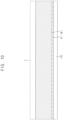
- Figure 1 is a plan view of a display device according to an embodiment of the present invention.
- a display device 10 may include a display area DA and a non-display area NDA.
- the display area DA may be an area for displaying an image.
- a planar shape of the display area DA may be a rectangular shape or a rectangular shape with rounded corners as shown in Figure 1 .
- the planar shape of the display area DA is not limited thereto, and the display area DA may have one or more suitable planar shapes such as a circle, an ellipse, and/or a polygon.
- the non-display area NDA may be disposed around the display area DA.
- the non-display area NDA may surround the display area DA.
- the non-display area NDA may be an area that does not display an image.
- drivers for displaying an image in the display area DA may be disposed in the non-display area NDA.
- Pixels PX may be arranged in a matrix in the display area DA.
- Signal lines such as a gate line GL and a data line DL may be disposed in the display area DA.
- the signal lines such as the gate line GL and the data line DL may be connected to each of the pixels PX.
- Each of the pixels PX may receive a gate signal, a data signal, and/or the like from the signal lines.
- the display device 10 may include a substrate 100, a display element layer 200, and an encapsulation layer 300.
- the display element layer 200 may include a circuit element layer 210 and a light emitting element layer 220.
- the circuit element layer 210 may be disposed on the substrate 100, and include a metal pattern BML, a buffer layer BFR, at least one transistor TR, a gate line, a connection electrode CP, and a first insulation layer IL1, a second insulation layer IL2, a third insulation layer IL3, and a fourth insulation layer IL4.
- the transistor TR may include an active layer ACT, a gate electrode GE, a source electrode SE, and a drain electrode DE.
- the light emitting element layer 220 may be disposed on the circuit element layer 210, and may include a fifth insulation layer IL5, a spacer SPC, and a light emitting diode LD.
- the light emitting diode LD may include a first electrode E1, a light emitting layer LEL, and a second electrode E2.
- the substrate 100 may support the display element layer 200.
- the substrate 100 may be a base substrate or a base member, and may be made of an insulating material such as a polymer resin.
- the substrate 100 may be a flexible substrate capable of bending, folding, rolling, and/or the like.
- the substrate 100 may include a flexible material and a rigid material.
- the metal pattern BML may be disposed on the substrate 100.
- the buffer layer BFR may be disposed on the substrate 100.
- the buffer layer BFR may cover the metal pattern BML.
- the metal pattern BML and the buffer layer BFR may prevent or reduce the diffusion of metal atoms or impurities from the substrate 100 into the active layer ACT.
- the active layer ACT may be disposed on the substrate 100.
- the active layer ACT may overlap the metal pattern BML.
- the active layer ACT may be divided into a source region and a drain region doped with impurities, and a channel region between the source region and the drain region.
- the active layer ACT may include an oxide semiconductor.
- the oxide semiconductor a single metal oxide such as indium (In) oxide, tin (Sn) oxide, or zinc (Zn) oxide, a binary metal oxide such as an In-Zn-based oxide, a Sn-Zn-based oxide, an Al-Zn-based oxide, a Zn-Mg-based oxide, a Sn-Mg-based oxide, an In-Mg-based oxide or In-Ga-based oxide, a ternary metal oxide such as an In-Ga-Zn-based oxide, an In-Al-Zn-based oxide, an In-Sn-Zn oxide, a Sn-Ga-Zn oxide, an Al-Ga-Zn oxide, a Sn-Al-Zn oxide, an In-Hf-Zn oxide, an In-La-Zn oxide, an In-Ce-Zn oxide, an In-Pr-Zn-based oxide, an In-Nd-Zn-based oxide,
- the first insulation layer IL1 may be disposed on the active layer ACT.
- the first insulation layer IL1 may overlap the active layer ACT and have an island shape.
- the present invention is not limited thereto.
- the first insulation layer IL1 may include an inorganic material.
- a gate layer including the gate line and the gate electrode GE may be disposed on the first insulation layer IL1.
- the gate electrode GE may overlap the channel region of the active layer ACT.
- the present invention is not limited thereto, and the gate electrode GE may be a portion of the gate line. Accordingly, the material forming the gate electrode GE and the thickness of the gate electrode GE may be the same as those of the gate line.
- the second insulation layer IL2 may be disposed on the buffer layer BFR and the active layer ACT.
- the second insulation layer IL2 may cover the active layer ACT, the first insulation layer IL1, and the gate electrode GE, and may be disposed to have substantially the same thickness along a profile of the active layer ACT, the first insulation layer IL1 and the gate electrode GE.
- the present invention is not limited thereto.
- the source electrode SE and the drain electrode DE may be disposed on the second insulation layer IL2.
- the source electrode SE may contact the metal pattern BML through a first contact hole formed in the buffer layer BFR and second insulation layer IL2.
- the source electrode SE may contact the source region of the active layer ACT through a second contact hole formed in the second insulation layer IL2.
- the drain electrode DE may contact the drain region of the active layer ACT through a third contact hole formed in the second insulation layer IL2.
- the present invention is not limited thereto.
- the drain electrode DE may contact the metal pattern BML through a first contact hole formed in the first and second insulation layer IL1 and IL2, and contact the active layer ACT through a second contact hole formed in the insulation layer IL2.
- the source electrode SE may contact the active layer ACT through a third contact hole formed in the second insulation layer IL2.
- the third insulation layer IL3 may be disposed on the second insulation layer IL2.
- the third insulation layer IL3 may cover the source and drain electrodes SE and DE, and have a substantially flat top surface without creating a step around the source and drain electrodes SE and DE.
- the third insulation layer IL3 may include an organic material.
- connection electrode CP may be disposed on the third insulation layer IL3.
- the connection electrode CP may contact the source electrode SE or the drain electrode DE through a fourth contact hole formed in the third insulation layer IL3.
- the fourth insulation layer IL4 may be disposed on the third insulation layer IL3.
- the fourth insulation layer IL4 may cover the connection electrode CP, and may have a substantially flat top surface without creating a step difference around the source and drain electrodes SE and DE.
- the fourth insulation layer IL4 may include an organic material.
- the first electrode E1 may be disposed on the fourth insulation layer IL4.
- the first electrode E1 may have reflective or transmissive properties.
- the first electrode E1 may include a metal.
- the first electrode E1 may contact the connection electrode CP through a fifth contact hole formed in the fourth insulation layer IL4. Through this, the first electrode E1 may be connected to the transistor TR.
- the fifth insulation layer IL5 may be disposed on the fourth insulation layer IL4, and an opening exposing the top surface of the first electrode E1 may be defined in the fifth insulation layer IL5.
- the fifth insulation layer IL5 may include an organic material or an inorganic material.
- the spacer SPC may be disposed on the fifth insulation layer IL5.
- the spacer SPC may include an organic material or an inorganic material.
- the spacer SPC may maintain a gap between the encapsulation layer 300 and the substrate 100.
- the spacer SPC may include a material different from that of the fifth insulation layer IL5.
- the spacer SPC may be formed after the fifth insulation layer IL5 is formed.
- the present invention is not limited thereto, and the spacer SPC may include the same material as the fifth insulation layer IL5.
- the fifth insulation layer IL5 and the spacer SPC may be concurrently (e.g., simultaneously) formed utilizing a halftone mask.
- the light emitting layer LEL may be disposed on the first electrode E1.
- the light emitting layer LEL may be disposed in the opening formed in the fifth insulation layer IL5.
- the light emitting layer LEL may have a multilayer structure including a hole injection layer, a hole transport layer, an organic emission layer, an electron transport layer, and an electron injection layer.
- the organic light emitting layer may include a light emitting material.
- the second electrode E2 may cover the light emitting layer LEL and may be disposed on the fifth insulation layer IL5 and the spacer SPC.
- the second electrode E2 may have a plate shape.
- the second electrode E2 may have transmissive or reflective properties.
- the second electrode E2 may include a metal.
- the encapsulation layer 300 may prevent or substantially prevent moisture and oxygen from penetrating into the light emitting diode LD from the outside.
- the encapsulation layer 300 may include a first inorganic encapsulation layer IEL1, an organic encapsulation layer OEL, and a second inorganic encapsulation layer IEL2.
- the first inorganic encapsulation layer IEL1 may be disposed on the second electrode E2 to have substantially the same thickness along a profile of the second electrode E2.
- the organic encapsulation layer OEL may be disposed on the first inorganic encapsulation layer IEL1, and may have a substantially flat top surface without creating a step around the first inorganic encapsulation layer IEL1.
- the second inorganic encapsulation layer IEL2 may be disposed on the organic encapsulation layer OEL.
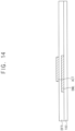
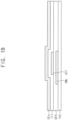
- Figure 3 is an enlarged cross-sectional view of area A of Figure 2 .
- Figure 4 is an enlarged cross-sectional view of area B of Figure 2 .
- Figure 3 is a cross-sectional view illustrating the metal pattern BML
- Figure 4 is a cross-sectional view illustrating the gate electrode GE.
- the metal pattern BML may include a first alloy layer AL1 and a first metal layer ML1.
- the first alloy layer AL1 may be disposed on the substrate 100, and the first metal layer ML1 may be disposed on the first alloy layer AL1.
- Each of the gate electrode GE and the gate line GL may include a second alloy layer AL2 and a second metal layer ML2.
- the second alloy layer AL2 may be disposed on the first insulation layer IL1, and the second metal layer ML2 may be disposed on the second alloy layer AL2.
- the gate electrode GE may be mainly described.
- the first metal layer ML1 and the second metal layer ML2 may include copper.
- the first metal layer ML1 and the second metal layer ML2 may include the same material.
- the first alloy layer AL1 may include a titanium alloy.
- the titanium alloy may include titanium (Ti), and at least one of copper (Cu) and/or zinc (Zn).
- the second alloy layer AL2 may include a titanium alloy.
- the titanium alloy may include titanium and may include at least one of copper and/or zinc.
- each of the first alloy layer AL1 and the second alloy layer AL2 may include a titanium alloy including titanium and copper.
- the present invention is not limited thereto, and each of the first alloy layer AL1 and the second alloy layer AL2 may include a titanium alloy including titanium and zinc.
- the first alloy layer AL1 and the second alloy layer AL2 may include the same material. However, the present invention is not limited thereto, and the first alloy layer AL1 and the second alloy layer AL2 may include different materials.
- the first alloy layer AL1 and the second alloy layer AL2 may include the same titanium alloy.
- the titanium alloy may include titanium and copper.
- a content of titanium included in the titanium alloy may be about 10 at% to about 80 at%.
- a content of copper included in the titanium alloy may be about 20 at% to about 90 at%.
- the second alloy layer AL2 including titanium may prevent or substantially prevent hydrogen from diffusing from the second insulation layer IL2 to the active layer ACT.
- the first alloy layer AL1 including titanium may prevent or substantially prevent hydrogen from diffusing from the substrate 100 to the active layer ACT.
- each of the first alloy layer AL1 and the second alloy layer AL2 may serve as a hydrogen barrier.
- a skew (e.g., skew SK1 of Figure 13 ) may increase when etching the first alloy layer AL1 and the first metal layer ML1.
- the skew refers to a distance between the end of the photoresist pattern (see, e.g., Figure 13 ) and the end of the metal pattern BML. Accordingly, it may be difficult to control a width of the metal pattern BML when the first alloy layer AL1 and the first metal layer ML1 are etched.
- a skew (e.g., skew SK2 of Figure 21 ) may increase, when the second alloy layer AL2 and the second metal layer ML2 are etched.
- the skew refers to a distance between the end of the photoresist pattern (see, e.g., Figure 21 ) and the end of the gate electrode GE. Accordingly, it may be difficult to control a width of the gate electrode GE when the second alloy layer AL2 and the second metal layer ML2 are etched.
- the content of titanium included in the titanium alloy may be about 20 at% to about 50 at%, and the content of copper included in the titanium alloy may be about 50 at% to about 80 at%.
- each of the first alloy layer AL1 and the second alloy layer AL2 may properly function as the hydrogen barrier. Also, because the difference between the etching rate of the titanium alloy and the etching rate of copper is reduced, the skew may be reduced when the first alloy layer AL1 and the first metal layer ML1 are etched. For example, when the first alloy layer AL1 and the first metal layer ML1 are etched, the width of the metal pattern BML may be controlled or selected (e.g., easily controlled or selected).
- the skew may be reduced.
- the width of the gate electrode GE may be controlled or selected (e.g., easily controlled or selected).
- each of the first alloy layer AL1 and the second alloy layer AL2 may include a titanium alloy including titanium, copper, and zinc.
- the titanium alloy may include all of titanium, copper, and zinc.
- the titanium alloy may include titanium and copper, but the present invention is not limited thereto. The same description may be applied to when the titanium alloy includes titanium and zinc, or the titanium alloy include titanium, copper, and zinc.
- each of a thickness T1 of the first alloy layer AL1 and a thickness T2 of the second alloy layer AL2 may be between about 30 ⁇ and about 100 ⁇ .
- the first alloy layer AL1 and the second alloy layer AL2 may have substantially the same thickness.
- the present invention is not limited thereto, and the first alloy layer AL1 and the second alloy layer AL2 may have different thicknesses.
- each of the thickness T1 of the first alloy layer AL1 and the thickness T2 of the second alloy layer AL2 is less than about 30 ⁇ , during the manufacturing process it may be difficult to control each of the thickness T1 of the first alloy layer AL1 and the thickness T2 of the second alloy layer AL2. Accordingly, the reliability of the display device 10 may be deteriorated.
- each of the thickness T1 of the first alloy layer AL1 and the thickness T2 of the second alloy layer AL2 is more than about 100 ⁇ , during the manufacturing process when each of the first alloy layer AL1 and the second alloy layer AL2 is etched, it may take a long time to etch. Accordingly, because manufacturing time of the display device 10 increases, manufacturing efficiency may decrease.
- each of the thickness T1 of the first alloy layer AL1 and the thickness T2 of the second alloy layer AL2 is about 100 ⁇ or more, during heat treatment in high temperatures, thermal diffusion between titanium of each of the first and second alloy layers AL1 and AL2 and copper of each of the first and second metal layers ML1 and ML2 may occur. Accordingly, a diffusion layer due to thermal diffusion between titanium and copper may be formed between the first alloy layer AL1 and the first metal layer ML1 and between the second alloy layer AL2 and the second metal layer ML2. As each of the thickness T1 of the first alloy layer AL1 and the thickness T2 of the second alloy layer AL2 increases, the diffusion layer due to the thermal diffusion may become thicker. In addition, as the diffusion layer becomes thicker, the resistance of each of the metal pattern BML and the gate electrode GE may increase.
- each of a thickness T3 of the first metal layer ML1 and a thickness T4 of the second metal layer ML2 may be between about 1500 ⁇ and about 4500 ⁇ .
- the first metal layer ML1 and the second metal layer ML2 may have substantially the same thickness.
- the present invention is not limited thereto, and the first metal layer ML1 and the second metal layer ML2 may have different thicknesses.
- each of the thickness T3 of the first metal layer ML1 and the thickness T4 of the second metal layer ML2 is less than about 1500 ⁇ , resistance of the first metal layer ML1 and the second metal layer ML2, respectively, may increase.
- each of the thickness T3 of the first metal layer ML1 and the thickness T4 of the second metal layer ML2 is more than about 4500 ⁇
- each of the first metal layer ML1 and the second metal layer ML2 may affect layers disposed on each of the first metal layer ML1 and the second metal layer ML2 in the stacked structure of the display device 10. Accordingly, due to this, a defect may occur in the display device 10.
- the first alloy layer AL1 and the second alloy layer AL2 include the same material, and the first metal layer ML1 and the second metal layer ML2 include the same material, thus the metal pattern BML may include substantially the same material as the gate electrode GE.
- a thickness T5 of the metal pattern BML may be substantially the same as a thickness T6 of the gate electrode GE.
- the metal pattern BML and the gate electrode GE may be connected to the gate line GL.
- the metal pattern BML includes substantially the same material as the gate electrode GE and the gate line GL, and the thickness T5 of the metal pattern BML, the thickness T6 of the gate electrode GE, and a thickness of the gate line GL are substantially the same, the metal pattern BML, the gate electrode GE, and the gate line GL may have substantially the same resistance. Accordingly, signal transmission through the gate line may be facilitated. Also, because the metal pattern BML, the gate electrode GE, and the gate line are formed of the same material and the same thickness, compatibility may be improved. Accordingly, it may be easy to manufacture the metal pattern BML, the gate electrode GE, and the gate line during the manufacturing process of the display device 10.
- the width of each of the metal pattern BML and the gate electrode GE may be controlled or selected (e.g., easily controlled or selected). Accordingly, a fine line width of each of the metal pattern BML and the gate electrode GE included in the display device 10 may be realized.
- the metal pattern BML and the gate electrode GE prevent or substantially prevent hydrogen from diffusing into the active layer ACT, thereby improving the performance of the transistor TR. Accordingly, a high resolution may be realized and display quality may be improved in the display device 10 including the metal pattern BML and the gate electrode GE.
- each of the first metal layer ML1 and the second metal layer ML2 includes copper, the resistance of the electrode and the wiring including the first metal layer ML1 and the second metal layer ML2 may be reduced.
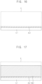
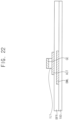
- Figure 5(a) is a graph illustrating bottom skew according to a thickness of the wiring for the wiring according to Examples and Comparative Examples.
- Figure 5(b) is a graph illustrating top skew according to the thickness of the wiring for the wiring according to Examples and Comparative Examples.
- a first layer e.g., the first alloy layer AL1 of Figure 3 or the second alloy layer AL2 of Figure 4 ) including about 50 at% titanium and about 50 at% copper and a second layer (e.g., the first metal layer ML1 of Figure 3 or the second metal layer ML2 of Figure 4 ) including copper on the first layer were prepared, and then the first layer and the second layer were wet-etched to prepare wiring.
- a first layer including titanium and a second layer including copper were prepared, and then the first layer and the second layer were wet-etched to prepare wiring.
- a thickness of the first layer and a thickness of the second layer according to each of the Examples and Comparative Examples are shown in Table 1. Table 1 Thickness of first layer ( ⁇ ) Thickness of second layer ( ⁇ ) Example 1 50 2500 Example 2 100 2500 Comparative Example 1 50 2500 Comparative Example 2 100 2500
- skew refers to a distance between an end of a photoresist pattern and an end of a bottom surface of the second layer in Figure 5(a) , and refers to a distance (e.g., the skew SK1 of Figure 13 and the skew SK2 of Figure 21 ) between an end of the photoresist pattern and an end of a top surface of the second layer in Figure 5(b) .
- the display device includes the first layer including the titanium-copper alloy, the skew of the second layer is reduced. Accordingly, it can be seen that it is relatively easy to control the width of the wiring of Examples 1 and 2 compared to the wiring of Comparative Examples 1 and 2.
- a first layer including about 50 at% titanium and about 50 at% copper and a second layer including copper on the first layer are prepared, and then the first layer and the second layer were wet-etched to prepare a wiring.
- the thickness of the first layer, the thickness of the second layer, and the width of the top surface of the second layer according to each of the Examples and the Comparative Examples are shown in Table 2.
- Table 2 A thickness of a first layer ( ⁇ ) A thickness of a second layer ( ⁇ ) A width of a top surface of a second layer ( ⁇ m)
- the width of the top surface of the second layer decreases relatively less.
- the skew decreases as the thickness of the first layer decreases. Accordingly, it can be seen that it is relatively easy to control the width of the wiring of Examples 1 and 2 compared to the wiring of Comparative Examples 3 and 4.
- Figure 6 is a graph illustrating sheet resistance values of wirings based on the thickness of the wiring according to Examples and Comparative Examples.
- a first layer including about 50 at% titanium and about 50 at% copper and a second layer including copper on the first layer were prepared, and then the first layer and the second layer were heat-treated at 400°C for 1 hour to prepare a wiring.
- the thickness of the first layer and the thickness of the second layer according to each of the Examples and Comparative Examples are shown in Table 3.
- Table 3 A thickness of a first layer ( ⁇ ) A thickness of a second layer ( ⁇ ) Example 3 30 2200
- the sheet resistance value after the heat treatment of the wiring satisfying each of Examples 3 to 6 is less than or substantially the same as the sheet resistance value before the heat treatment of the wiring.
- the sheet resistance value after heat treatment of the wiring of Comparative Examples 5 and 6 is greater than the sheet resistance value before the heat treatment of the wiring.
- Figure 7 is a graph illustrating driving currents (IDS) according to gate-source voltages (VGS) of transistors according to Examples and Comparative Examples.
- a first layer including about 50 at% titanium and about 50 at% copper and a second layer including copper on the first layer were prepared, and then the first layer and the second layer were wet-etched to prepare a gate electrode, and a transistor including the gate electrode was prepared.
- a first layer including titanium and a second layer including molybdenum (Mo) on the first layer were prepared, and then the first layer and the second layer were wet-etched to form a gate electrode and a transistor including the gate electrode was prepared.
- Mo molybdenum
- a first layer including titanium and a second layer including copper on the first layer were prepared, and then the first layer and the second layer were wet-etched to form a gate electrode and a transistor including the gate electrode was prepared.
- the first layer was formed to a thickness of about 100 ⁇ .
- Example 7 In the driving current of Example 7, it can be seen that a dispersion is smaller than the driving current satisfying Comparative Examples 7 and 8. Through these results, it can be seen that the gate electrode of Example 7 of the present invention has improved transistor performance compared to the gate electrode of Comparative Examples 7 and 8.
- Figures 8 to 26 are cross-sectional views illustrating a method of manufacturing a display device according to an embodiment of the present invention.
- Figures 8 to 26 may be views for explaining a method of manufacturing the display device described with reference to Figures 1 to 4 . Therefore, the overlapping description may not be provided.
- Figures 9 and 10 are cross-sectional views illustrating a stacking sequence by enlarging area C of Figure 8 .
- a first alloy layer AL1 may be formed on the substrate 100, and a first metal layer ML1 may be formed on the first alloy layer AL1.
- the first alloy layer AL1 and the first metal layer ML1 may form a raw metal layer BMLa.
- the first alloy layer AL1 may be formed of a titanium alloy including at least one of copper and/or zinc.
- the first metal layer ML1 may be formed of copper.
- the titanium alloy may be formed of titanium and at least one of copper and/or zinc.
- the titanium alloy may be formed of titanium and copper.
- the content of titanium forming the titanium alloy may be about 10 at% to about 80 at%.
- the content of copper forming the titanium alloy may be about 20 at% to about 90 at%.
- the content of titanium forming the titanium alloy may be about 20 at% to about 50 at%, and the content of copper forming the titanium alloy may be about 50 at% to about 80 at%.
- a first photoresist pattern PR1 may be formed on the raw metal layer BMLa.
- the first alloy layer AL1 and the first metal layer ML1 may be patterned utilizing the first photoresist pattern PR1.
- the raw metal layer BMLa may be patterned to form a metal pattern BML.
- the first alloy layer AL1 and the first metal layer ML1 may be etched utilizing a wet etching technique.
- Figure 13 is an enlarged cross-sectional view of area D of Figure 12 .
- the thickness T1 of the first alloy layer AL1 may be between about 30 ⁇ and about 100 ⁇ .
- the width of the metal pattern BML may be controlled or selected (e.g., easily controlled or selected) during a manufacturing process, and an etching time of the first alloy layer AL1 is reduced, so that the manufacturing time of the display device 10 is reduced, and thus manufacturing efficiency may be increased.
- the thickness T3 of the first metal layer ML1 may be between about 1500 ⁇ and about 4500 ⁇ .
- the first metal layer ML1 may have little influence on the layers disposed on the first metal layer ML 1.
- the resistance of the first metal layer ML1 may be relatively small.
- etching rates of the first metal layer ML1 and the first alloy layer AL1 may be similar to each other. Accordingly, a skew SK1, which is a distance between the end of the first photoresist pattern PR1 and the end of the gate electrode GE (or the gate line), may decrease.
- the first photoresist pattern PR1 may be removed.
- a buffer layer BFR may be formed on the metal pattern BML.
- the buffer layer BFR may be formed to cover the metal pattern BML.
- An active layer ACT may be formed on the buffer layer BFR.
- the active layer ACT may be formed of an oxide semiconductor.
- the active layer ACT may be formed of Indium-Gallium-Zinc Oxide (IGZO).
- IGZO Indium-Gallium-Zinc Oxide
- a first insulation layer IL1 may be formed on the active layer ACT.
- the first insulation layer IL1 may be formed to cover the active layer ACT.
- Figures 16 and 17 are cross-sectional views illustrating a stacking sequence by enlarging area E of Figure 15 .
- a second alloy layer AL2 may be formed on the active layer ACT, and a second metal layer ML2 may be formed on the second alloy layer AL2.
- the second alloy layer AL2 may be formed of a titanium alloy including at least one of copper and/or zinc.
- the second metal layer ML2 may be formed of copper.
- the second alloy layer AL2 and the second metal layer ML2 may form a gate layer GEa.
- the titanium alloy may be formed of titanium and at least one of copper and/or zinc.
- the titanium alloy may be formed of titanium and copper.
- the content of titanium forming the titanium alloy may be about 10 at% to about 80 at%.
- the content of copper forming the titanium alloy may be about 20 at% to about 90 at%.
- the content of titanium forming the titanium alloy may be about 20 at% to about 50 at%, and the content of copper forming the titanium alloy may be about 50 at% to about 80 at%.
- a second photoresist pattern PR2 may be formed on the gate layer GEa.
- the second alloy layer AL2 and the second metal layer ML2 may be patterned utilizing the second photoresist pattern PR2.
- the gate layer GEa may be patterned to form a gate electrode GE and a gate line GL.
- the second alloy layer AL2 and the second metal layer ML2 may be etched utilizing a wet etching technique.
- Figure 21 is an enlarged cross-sectional view of area F of Figure 20 .
- the thickness T2 of the second alloy layer AL2 may be between about 30 ⁇ and about 100 ⁇ .
- the width of each of the gate electrode GE and the gate line GL may be controlled or selected (e.g., easily controlled or selected) during a manufacturing process, and the width of the second alloy layer AL2 may be controlled or selected (e.g., easily controlled or selected). Because the etching time of the second alloy layer AL2 is reduced, the manufacturing time of the display device 10 is decreased, and thus manufacturing efficiency may be increased.
- the thickness T4 of the second metal layer ML2 may be between about 1500 ⁇ and about 4500 ⁇ .
- the second metal layer ML2 may have little effect on the layers disposed on the second metal layer ML2.
- the resistance of the second metal layer ML2 may be relatively small.
- etching rates of the second metal layer ML2 and the second alloy layer AL2 may be similar to each other. Accordingly, a skew SK2 that is a distance between the end of the second photoresist pattern PR2 and the end of the gate electrode GE (or the gate line GL) may be reduced.
- the thickness T5 of the metal pattern BML and the thickness T6 of the gate electrode GE may be substantially the same as each other. Because the thickness T5 of the metal pattern BML and the thickness T6 of the gate electrode GE are substantially the same, the metal pattern BML and the gate electrode GE may have substantially the same resistance.
- the second photoresist pattern PR2 may be removed.
- the first insulation layer IL1 may be patterned. A portion of the first insulation layer IL1 that does not overlap the gate electrode GE and the gate line GL may be etched. Accordingly, the first insulation layer IL1 may overlap the gate electrode GE and the gate line GL.
- the present invention is not limited thereto, and the first insulation layer IL1 may be entirely formed on the buffer layer BFR.
- a second insulation layer IL2 may be formed on the buffer layer BFR and the active layer ACT.
- the second insulation layer IL2 may be formed to cover the active layer ACT, the first insulation layer IL1, and the gate electrode GE.
- a first contact hole may be formed in the buffer layer BFR and the second insulation layer IL2, and a second contact hole and a third contact hole may be formed in the second insulation layer IL2.
- a source electrode SE and a drain electrode DE may be formed on the second insulation layer IL2.
- the source electrode SE may contact the metal pattern BML through the first contact hole, and may contact the source region of the active layer ACT through the second contact hole.
- the drain electrode DE may contact the drain region of the active layer ACT through the third contact hole.
- the active layer ACT, the gate electrode GE, the source electrode SE, and the drain electrode DE may form a transistor TR.
- a third insulation layer IL3 may be formed on the second insulation layer IL2 to cover the source electrode SE and the drain electrode DE.
- a fourth contact hole may be formed in the third insulation layer IL3.
- a connection electrode CP may be formed on the third insulation layer IL3, and the connection electrode CP may contact the drain electrode DE through the fourth contact hole.
- a fourth insulation layer IL4 may be formed on the third insulation layer IL3 to cover the connection electrode CP. Accordingly, a circuit element layer 210 may be formed.
- a light emitting element layer 220 may be formed on the fourth insulation layer IL4.
- the circuit element layer 210 and the light emitting element layer 220 may form the display element layer 200.
- An encapsulation layer 300 may be formed on the light emitting element layer 220. Accordingly, the display device 10 including the substrate 100, the display element layer 200, and the encapsulation layer 300 may be formed.
- the first alloy layer AL1 includes the titanium alloy
- etching rates of the first metal layer ML1 and the first alloy layer AL1 may be similar to each other. Accordingly, the skew SK1, which is the distance between the end of the first photoresist pattern PR1 and the end of the metal pattern BML may be reduced, and the width of the metal pattern BML may be controlled or selected (e.g., easily controlled or selected).
- etching rates of the second metal layer ML2 and the second alloy layer AL2 may be similar to each other.
- the skew SK2 which is the distance between the end of the second photoresist pattern PR2 and the end of the gate electrode GE (or the gate line), may be reduced, and the width of the gate electrode GE may be controlled or selected (e.g., easily controlled or selected). Accordingly, a high resolution may be realized in the display device 10.
- the first alloy layer AL1 and the second alloy layer AL2 include the titanium alloy
- the first alloy layer AL1 and the second alloy layer AL2 may prevent or substantially prevent hydrogen from diffusing into the active layer ACT. Accordingly, the performance of the transistor TR may be improved.
- the display devices according to the embodiments may be applied to a display device included in a computer, a notebook, a mobile phone, a smartphone, a smart pad, a PMP, a PDA, an MP3 player, and/or the like.
Landscapes
- Engineering & Computer Science (AREA)
- Microelectronics & Electronic Packaging (AREA)
- Manufacturing & Machinery (AREA)
- Physics & Mathematics (AREA)
- Geometry (AREA)
- Devices For Indicating Variable Information By Combining Individual Elements (AREA)
- Thin Film Transistor (AREA)
- Electroluminescent Light Sources (AREA)
- Laminated Bodies (AREA)
Applications Claiming Priority (2)
| Application Number | Priority Date | Filing Date | Title |
|---|---|---|---|
| KR1020220074866A KR20230174346A (ko) | 2022-06-20 | 2022-06-20 | 표시 장치 및 이의 제조 방법 |
| PCT/KR2023/006279 WO2023249249A1 (fr) | 2022-06-20 | 2023-05-09 | Dispositif d'affichage et procédé de fabrication associé |
Publications (1)
| Publication Number | Publication Date |
|---|---|
| EP4543177A1 true EP4543177A1 (fr) | 2025-04-23 |
Family
ID=89054576
Family Applications (1)
| Application Number | Title | Priority Date | Filing Date |
|---|---|---|---|
| EP23827369.2A Pending EP4543177A1 (fr) | 2022-06-20 | 2023-05-09 | Dispositif d'affichage et procédé de fabrication associé |
Country Status (6)
| Country | Link |
|---|---|
| US (1) | US12453264B2 (fr) |
| EP (1) | EP4543177A1 (fr) |
| JP (1) | JP2025523415A (fr) |
| KR (1) | KR20230174346A (fr) |
| CN (2) | CN117279436A (fr) |
| WO (1) | WO2023249249A1 (fr) |
Families Citing this family (1)
| Publication number | Priority date | Publication date | Assignee | Title |
|---|---|---|---|---|
| CN113966551A (zh) * | 2020-03-25 | 2022-01-21 | 京东方科技集团股份有限公司 | 显示基板和显示装置 |
Family Cites Families (20)
| Publication number | Priority date | Publication date | Assignee | Title |
|---|---|---|---|---|
| JP3974305B2 (ja) | 1999-06-18 | 2007-09-12 | エルジー フィリップス エルシーディー カンパニー リミテッド | エッチング剤及びこれを用いた電子機器用基板の製造方法と電子機器 |
| US7973319B2 (en) | 2003-09-19 | 2011-07-05 | Sony Corporation | Display unit, method of manufacturing same, organic light emitting unit, and method of manufacturing same |
| KR20060012764A (ko) | 2004-08-04 | 2006-02-09 | 삼성전자주식회사 | 박막 표시판 및 그 제조 방법 |
| KR101716471B1 (ko) | 2010-06-07 | 2017-03-28 | 삼성디스플레이 주식회사 | 유기 발광 표시 장치 및 그 제조 방법 |
| KR101895421B1 (ko) * | 2011-02-24 | 2018-09-07 | 삼성디스플레이 주식회사 | 배선, 박막 트랜지스터, 및 박막 트랜지스터 표시판과 이들을 제조하는 방법들 |
| WO2013046606A1 (fr) | 2011-09-27 | 2013-04-04 | 凸版印刷株式会社 | Transistor à couche mince et appareil d'affichage d'image |
| KR102165616B1 (ko) | 2013-08-29 | 2020-10-15 | 엘지디스플레이 주식회사 | 평판 표시장치 |
| KR102251840B1 (ko) | 2014-08-14 | 2021-05-13 | 엘지디스플레이 주식회사 | 저반사 패널을 포함하는 유기발광 표시장치 |
| KR102224029B1 (ko) | 2014-08-22 | 2021-03-09 | 엘지디스플레이 주식회사 | 유기발광표시패널 및 표시장치 |
| KR102132393B1 (ko) | 2014-08-22 | 2020-07-10 | 엘지디스플레이 주식회사 | 유기발광 표시장치 |
| KR20170064606A (ko) | 2015-12-01 | 2017-06-12 | 엘지디스플레이 주식회사 | 유기발광 표시패널 및 이를 포함하는 유기발광 표시장치 |
| KR102567323B1 (ko) | 2016-10-06 | 2023-08-16 | 엘지디스플레이 주식회사 | 차광 패턴을 포함하는 디스플레이 장치 |
| KR102753554B1 (ko) | 2016-12-28 | 2025-01-10 | 엘지디스플레이 주식회사 | 불규칙한 박막층을 포함하는 표시장치 |
| KR102297897B1 (ko) | 2017-04-25 | 2021-09-03 | 엘지디스플레이 주식회사 | 다중층의 패드부를 포함하는 기판, 기판을 포함하는 표시패널 및 이를 제조하는 방법 |
| KR102365029B1 (ko) | 2017-07-28 | 2022-02-17 | 엘지디스플레이 주식회사 | 전계 발광 표시장치 |
| KR20210004356A (ko) | 2019-07-04 | 2021-01-13 | 엘지디스플레이 주식회사 | 산화물 반도체 패턴을 포함하는 디스플레이 장치 |
| KR102662200B1 (ko) | 2019-07-15 | 2024-04-29 | 엘지디스플레이 주식회사 | 유기발광표시장치 |
| KR102839061B1 (ko) * | 2020-06-25 | 2025-07-28 | 삼성디스플레이 주식회사 | 표시 장치와 그의 제조 방법 |
| KR102698618B1 (ko) | 2020-10-20 | 2024-08-27 | 엘지디스플레이 주식회사 | 박막 트랜지스터 어레이 기판 및 이를 포함하는 전자장치 |
| JP7682665B2 (ja) * | 2021-03-29 | 2025-05-26 | キヤノン株式会社 | 発光装置、表示装置、撮像装置、及び、電子機器 |
-
2022
- 2022-06-20 KR KR1020220074866A patent/KR20230174346A/ko active Pending
-
2023
- 2023-02-10 US US18/108,518 patent/US12453264B2/en active Active
- 2023-05-09 WO PCT/KR2023/006279 patent/WO2023249249A1/fr not_active Ceased
- 2023-05-09 JP JP2024572502A patent/JP2025523415A/ja active Pending
- 2023-05-09 EP EP23827369.2A patent/EP4543177A1/fr active Pending
- 2023-06-16 CN CN202310720647.0A patent/CN117279436A/zh active Pending
- 2023-06-16 CN CN202321539460.2U patent/CN220173711U/zh active Active
Also Published As
| Publication number | Publication date |
|---|---|
| JP2025523415A (ja) | 2025-07-23 |
| WO2023249249A1 (fr) | 2023-12-28 |
| US12453264B2 (en) | 2025-10-21 |
| CN220173711U (zh) | 2023-12-12 |
| KR20230174346A (ko) | 2023-12-28 |
| US20230413631A1 (en) | 2023-12-21 |
| CN117279436A (zh) | 2023-12-22 |
Similar Documents
| Publication | Publication Date | Title |
|---|---|---|
| US11271015B2 (en) | Display device | |
| US11227875B2 (en) | Display device | |
| US11462602B2 (en) | Array substrate, manufacturing method thereof, and display device | |
| US11823628B2 (en) | Display device | |
| US12069918B2 (en) | Display device and method for fabricating the same | |
| KR102740671B1 (ko) | 표시 장치 및 그 제조 방법 | |
| US20250040194A1 (en) | Thin Film Transistor Array Substrate and Display Device | |
| KR20210021218A (ko) | 표시 장치 | |
| US7170225B2 (en) | Flat panel display for displaying screens at both sides | |
| KR20210040202A (ko) | 표시 장치 | |
| US20200052053A1 (en) | Display Substrate, Fabricating Method Thereof, and Display Device | |
| KR20210010696A (ko) | 표시 장치 | |
| KR102407538B1 (ko) | 유기발광다이오드 표시장치 및 그 제조 방법 | |
| EP4543177A1 (fr) | Dispositif d'affichage et procédé de fabrication associé | |
| KR20220149879A (ko) | 표시 장치 | |
| CN112714960B (zh) | 显示装置 | |
| US12588380B2 (en) | Display device | |
| US20240341132A1 (en) | Display device | |
| KR20110097121A (ko) | 어레이 기판 | |
| CN113345916A (zh) | 显示面板及其制备方法 | |
| US12550566B2 (en) | Display panel with auxiliary layer, method for preparing same, and display device | |
| US20260006990A1 (en) | Display device, method of fabricating display device, and electronic device including the same | |
| KR102940197B1 (ko) | 표시 장치 및 표시 장치의 제조 방법 | |
| US20250228076A1 (en) | Display Device | |
| US20250254995A1 (en) | Thin-film transistor array substrate and display device including same |
Legal Events
| Date | Code | Title | Description |
|---|---|---|---|
| STAA | Information on the status of an ep patent application or granted ep patent |
Free format text: STATUS: THE INTERNATIONAL PUBLICATION HAS BEEN MADE |
|
| PUAI | Public reference made under article 153(3) epc to a published international application that has entered the european phase |
Free format text: ORIGINAL CODE: 0009012 |
|
| STAA | Information on the status of an ep patent application or granted ep patent |
Free format text: STATUS: REQUEST FOR EXAMINATION WAS MADE |
|
| 17P | Request for examination filed |
Effective date: 20241206 |
|
| AK | Designated contracting states |
Kind code of ref document: A1 Designated state(s): AL AT BE BG CH CY CZ DE DK EE ES FI FR GB GR HR HU IE IS IT LI LT LU LV MC ME MK MT NL NO PL PT RO RS SE SI SK SM TR |
|
| DAV | Request for validation of the european patent (deleted) | ||
| DAX | Request for extension of the european patent (deleted) | ||
| P01 | Opt-out of the competence of the unified patent court (upc) registered |
Free format text: CASE NUMBER: UPC_APP_0007588_4543177/2026 Effective date: 20260226 |