EP4546175A2 - Chip, verfahren zur erzeugung privater schlüssel und vertrauenswürdiges zertifizierungsverfahren - Google Patents
Chip, verfahren zur erzeugung privater schlüssel und vertrauenswürdiges zertifizierungsverfahren Download PDFInfo
- Publication number
- EP4546175A2 EP4546175A2 EP24220444.4A EP24220444A EP4546175A2 EP 4546175 A2 EP4546175 A2 EP 4546175A2 EP 24220444 A EP24220444 A EP 24220444A EP 4546175 A2 EP4546175 A2 EP 4546175A2
- Authority
- EP
- European Patent Office
- Prior art keywords
- layer
- firmware
- security core
- chip
- memory
- Prior art date
- Legal status (The legal status is an assumption and is not a legal conclusion. Google has not performed a legal analysis and makes no representation as to the accuracy of the status listed.)
- Pending
Links
Images




Classifications
-
- H—ELECTRICITY
- H04—ELECTRIC COMMUNICATION TECHNIQUE
- H04L—TRANSMISSION OF DIGITAL INFORMATION, e.g. TELEGRAPHIC COMMUNICATION
- H04L9/00—Cryptographic mechanisms or cryptographic arrangements for secret or secure communications; Network security protocols
- H04L9/32—Cryptographic mechanisms or cryptographic arrangements for secret or secure communications; Network security protocols including means for verifying the identity or authority of a user of the system or for message authentication, e.g. authorization, entity authentication, data integrity or data verification, non-repudiation, key authentication or verification of credentials
- H04L9/3263—Cryptographic mechanisms or cryptographic arrangements for secret or secure communications; Network security protocols including means for verifying the identity or authority of a user of the system or for message authentication, e.g. authorization, entity authentication, data integrity or data verification, non-repudiation, key authentication or verification of credentials involving certificates, e.g. public key certificate [PKC] or attribute certificate [AC]; Public key infrastructure [PKI] arrangements
- H04L9/3265—Cryptographic mechanisms or cryptographic arrangements for secret or secure communications; Network security protocols including means for verifying the identity or authority of a user of the system or for message authentication, e.g. authorization, entity authentication, data integrity or data verification, non-repudiation, key authentication or verification of credentials involving certificates, e.g. public key certificate [PKC] or attribute certificate [AC]; Public key infrastructure [PKI] arrangements using certificate chains, trees or paths; Hierarchical trust model
-
- H—ELECTRICITY
- H04—ELECTRIC COMMUNICATION TECHNIQUE
- H04L—TRANSMISSION OF DIGITAL INFORMATION, e.g. TELEGRAPHIC COMMUNICATION
- H04L9/00—Cryptographic mechanisms or cryptographic arrangements for secret or secure communications; Network security protocols
- H04L9/08—Key distribution or management, e.g. generation, sharing or updating, of cryptographic keys or passwords
- H04L9/0894—Escrow, recovery or storing of secret information, e.g. secret key escrow or cryptographic key storage
- H04L9/0897—Escrow, recovery or storing of secret information, e.g. secret key escrow or cryptographic key storage involving additional devices, e.g. trusted platform module [TPM], smartcard or USB
-
- G—PHYSICS
- G06—COMPUTING OR CALCULATING; COUNTING
- G06F—ELECTRIC DIGITAL DATA PROCESSING
- G06F21/00—Security arrangements for protecting computers, components thereof, programs or data against unauthorised activity
- G06F21/50—Monitoring users, programs or devices to maintain the integrity of platforms, e.g. of processors, firmware or operating systems
- G06F21/57—Certifying or maintaining trusted computer platforms, e.g. secure boots or power-downs, version controls, system software checks, secure updates or assessing vulnerabilities
-
- G—PHYSICS
- G06—COMPUTING OR CALCULATING; COUNTING
- G06F—ELECTRIC DIGITAL DATA PROCESSING
- G06F21/00—Security arrangements for protecting computers, components thereof, programs or data against unauthorised activity
- G06F21/70—Protecting specific internal or peripheral components, in which the protection of a component leads to protection of the entire computer
- G06F21/71—Protecting specific internal or peripheral components, in which the protection of a component leads to protection of the entire computer to assure secure computing or processing of information
- G06F21/72—Protecting specific internal or peripheral components, in which the protection of a component leads to protection of the entire computer to assure secure computing or processing of information in cryptographic circuits
-
- H—ELECTRICITY
- H04—ELECTRIC COMMUNICATION TECHNIQUE
- H04L—TRANSMISSION OF DIGITAL INFORMATION, e.g. TELEGRAPHIC COMMUNICATION
- H04L9/00—Cryptographic mechanisms or cryptographic arrangements for secret or secure communications; Network security protocols
- H04L9/08—Key distribution or management, e.g. generation, sharing or updating, of cryptographic keys or passwords
- H04L9/0816—Key establishment, i.e. cryptographic processes or cryptographic protocols whereby a shared secret becomes available to two or more parties, for subsequent use
- H04L9/0819—Key transport or distribution, i.e. key establishment techniques where one party creates or otherwise obtains a secret value, and securely transfers it to the other(s)
- H04L9/0825—Key transport or distribution, i.e. key establishment techniques where one party creates or otherwise obtains a secret value, and securely transfers it to the other(s) using asymmetric-key encryption or public key infrastructure [PKI], e.g. key signature or public key certificates
-
- H—ELECTRICITY
- H04—ELECTRIC COMMUNICATION TECHNIQUE
- H04L—TRANSMISSION OF DIGITAL INFORMATION, e.g. TELEGRAPHIC COMMUNICATION
- H04L9/00—Cryptographic mechanisms or cryptographic arrangements for secret or secure communications; Network security protocols
- H04L9/08—Key distribution or management, e.g. generation, sharing or updating, of cryptographic keys or passwords
- H04L9/0861—Generation of secret information including derivation or calculation of cryptographic keys or passwords
- H04L9/0877—Generation of secret information including derivation or calculation of cryptographic keys or passwords using additional device, e.g. trusted platform module [TPM], smartcard, USB or hardware security module [HSM]
-
- H—ELECTRICITY
- H04—ELECTRIC COMMUNICATION TECHNIQUE
- H04L—TRANSMISSION OF DIGITAL INFORMATION, e.g. TELEGRAPHIC COMMUNICATION
- H04L9/00—Cryptographic mechanisms or cryptographic arrangements for secret or secure communications; Network security protocols
- H04L9/08—Key distribution or management, e.g. generation, sharing or updating, of cryptographic keys or passwords
- H04L9/0891—Revocation or update of secret information, e.g. encryption key update or rekeying
-
- H—ELECTRICITY
- H04—ELECTRIC COMMUNICATION TECHNIQUE
- H04L—TRANSMISSION OF DIGITAL INFORMATION, e.g. TELEGRAPHIC COMMUNICATION
- H04L9/00—Cryptographic mechanisms or cryptographic arrangements for secret or secure communications; Network security protocols
- H04L9/32—Cryptographic mechanisms or cryptographic arrangements for secret or secure communications; Network security protocols including means for verifying the identity or authority of a user of the system or for message authentication, e.g. authorization, entity authentication, data integrity or data verification, non-repudiation, key authentication or verification of credentials
- H04L9/3236—Cryptographic mechanisms or cryptographic arrangements for secret or secure communications; Network security protocols including means for verifying the identity or authority of a user of the system or for message authentication, e.g. authorization, entity authentication, data integrity or data verification, non-repudiation, key authentication or verification of credentials using cryptographic hash functions
- H04L9/3242—Cryptographic mechanisms or cryptographic arrangements for secret or secure communications; Network security protocols including means for verifying the identity or authority of a user of the system or for message authentication, e.g. authorization, entity authentication, data integrity or data verification, non-repudiation, key authentication or verification of credentials using cryptographic hash functions involving keyed hash functions, e.g. message authentication codes [MACs], CBC-MAC or HMAC
-
- H—ELECTRICITY
- H04—ELECTRIC COMMUNICATION TECHNIQUE
- H04L—TRANSMISSION OF DIGITAL INFORMATION, e.g. TELEGRAPHIC COMMUNICATION
- H04L9/00—Cryptographic mechanisms or cryptographic arrangements for secret or secure communications; Network security protocols
- H04L9/32—Cryptographic mechanisms or cryptographic arrangements for secret or secure communications; Network security protocols including means for verifying the identity or authority of a user of the system or for message authentication, e.g. authorization, entity authentication, data integrity or data verification, non-repudiation, key authentication or verification of credentials
- H04L9/3247—Cryptographic mechanisms or cryptographic arrangements for secret or secure communications; Network security protocols including means for verifying the identity or authority of a user of the system or for message authentication, e.g. authorization, entity authentication, data integrity or data verification, non-repudiation, key authentication or verification of credentials involving digital signatures
-
- H—ELECTRICITY
- H04—ELECTRIC COMMUNICATION TECHNIQUE
- H04L—TRANSMISSION OF DIGITAL INFORMATION, e.g. TELEGRAPHIC COMMUNICATION
- H04L9/00—Cryptographic mechanisms or cryptographic arrangements for secret or secure communications; Network security protocols
- H04L9/32—Cryptographic mechanisms or cryptographic arrangements for secret or secure communications; Network security protocols including means for verifying the identity or authority of a user of the system or for message authentication, e.g. authorization, entity authentication, data integrity or data verification, non-repudiation, key authentication or verification of credentials
- H04L9/3263—Cryptographic mechanisms or cryptographic arrangements for secret or secure communications; Network security protocols including means for verifying the identity or authority of a user of the system or for message authentication, e.g. authorization, entity authentication, data integrity or data verification, non-repudiation, key authentication or verification of credentials involving certificates, e.g. public key certificate [PKC] or attribute certificate [AC]; Public key infrastructure [PKI] arrangements
-
- H—ELECTRICITY
- H04—ELECTRIC COMMUNICATION TECHNIQUE
- H04L—TRANSMISSION OF DIGITAL INFORMATION, e.g. TELEGRAPHIC COMMUNICATION
- H04L9/00—Cryptographic mechanisms or cryptographic arrangements for secret or secure communications; Network security protocols
- H04L9/32—Cryptographic mechanisms or cryptographic arrangements for secret or secure communications; Network security protocols including means for verifying the identity or authority of a user of the system or for message authentication, e.g. authorization, entity authentication, data integrity or data verification, non-repudiation, key authentication or verification of credentials
- H04L9/3271—Cryptographic mechanisms or cryptographic arrangements for secret or secure communications; Network security protocols including means for verifying the identity or authority of a user of the system or for message authentication, e.g. authorization, entity authentication, data integrity or data verification, non-repudiation, key authentication or verification of credentials using challenge-response
-
- H—ELECTRICITY
- H04—ELECTRIC COMMUNICATION TECHNIQUE
- H04L—TRANSMISSION OF DIGITAL INFORMATION, e.g. TELEGRAPHIC COMMUNICATION
- H04L2209/00—Additional information or applications relating to cryptographic mechanisms or cryptographic arrangements for secret or secure communication H04L9/00
- H04L2209/12—Details relating to cryptographic hardware or logic circuitry
Definitions
- This application relates to the field of information technologies, and more specifically, to a chip, a private key generation method, and a trusted certification method.
- Some chips in a computer device impose a relatively high requirement on security. Once malicious code is implanted into operating systems and/or applications (application, APP) that are run by these chips, an attacker can easily obtain control over the computer device or obtain data in the computer device.
- application application
- a baseboard management controller (baseboard management controller, BMC) in a server is such a chip that imposes a relatively high requirement on security.
- the BMC uses a network interface to implement functions, such as providing remote maintenance of the server and monitoring a running status of the server.
- the BMC may further obtain running status information of a central processing unit (central processing unit, CPU) inside the server.
- the BMC may further manage a basic input/output system (basic input output system, BIOS) inside the server.
- BIOS basic input output system
- a challenge device verifies certificates of firmware at all layers that is run by a chip, to ensure that the firmware run by the chip is trustworthy.
- a trusted certification process currently used in the industry has the following disadvantage: If a private key is leaked, an attacker can use the private key to sign firmware containing malicious code. Therefore, a method for ensuring private key security is needed.
- This application provides a chip, a private key generation method, and a trusted certification method, to reduce a probability that an attacker obtains a private key and performs trusted certification on tampered firmware or information by using the private key.
- an embodiment of this application provides a chip.
- the chip includes a security core module, the security core module includes a security core and a memory, the security core module prevents access of an external module that is inside the chip and that is other than the security core module, and the security core module prevents access of an external device outside the chip;
- the memory is configured to store a hash of a first root public key and a unique device secret UDS of the chip; the security core is configured to generate a layer 1 public key and a layer 1 private key based on the hash of the first root public key and the UDS; and the memory is configured to store the layer 1 private key.
- the layer 1 private key is stored in the memory in the security core module, and the security core module prevents external access, a component outside the security core module cannot access the memory that stores the layer 1 private key. This can reduce a possibility that an attacker obtains the layer 1 private key and performs trusted certification on tampered firmware or information by using the layer 1 private key.
- the security core module is integrated into the chip, production costs of the chip are relatively low, and there is a relatively low requirement on layout space of a circuit board in which the chip is disposed.
- an address of the security core module is beyond an address range that is accessible by the external module and the external device. According to the foregoing technical solution, a component inside the security core module cannot be accessed by the component outside the security core module.
- the memory is further configured to store a hash of a second root public key; the security core is further configured to generate a layer 2 public key and a layer 2 private key based on the hash of the second root public key and the UDS; the memory is further configured to store the layer 2 private key; and the security core is further configured to sign a layer 2 certificate by using the layer 1 private key, where the layer 2 certificate includes the layer 2 public key.
- security core firmware includes only layer 1 firmware and layer 2 firmware and has a simple running environment, but can still implement a trusted certification process for firmware or data.
- the security core is further configured to delete the layer 1 private key after signing the layer 2 certificate by using the layer 1 private key. This can avoid forging the layer 2 certificate due to leakage of the layer 1 private key.
- the security core is further configured to: run secure firmware when receiving verification request information that is specific to target data and that is sent by a challenge device, to sign the target data based on the layer 2 private key; and send the signed target data to the challenge device, so that the challenge device verifies the signed target data based on the layer 2 public key.
- trusted certification can be implemented by using the security core.
- the security core is further configured to: run secure firmware when receiving verification request information that is specific to target data and that is sent by a challenge device, to sign the target data based on the layer 1 private key; and send the signed target data to the challenge device, so that the challenge device verifies the signed target data based on the layer 1 public key.
- trusted certification can be implemented by using the security core.
- the chip further includes a service core, configured to run service core firmware.
- a service core configured to run service core firmware.
- the chip further includes a first input/output interface and a second input/output interface, the first input/output interface is coupled to the security core module, and the second input/output interface is coupled to the service core.
- the security core module and the service core do not have common communications interfaces, and the security core can be further isolated from the service core.
- an embodiment of this application provides a private key generation method, where the method is performed by a security core in a chip.
- the security core is located in a security core module inside the chip, the security core module further includes a memory configured to store a hash of a first root public key and a unique device secret UDS of the chip, the security core module prevents access of an external module that is inside the chip and that is other than the security core module, and the security core module prevents access of an external device outside the chip.
- the method includes: obtaining, by the security core, the hash of the first root public key and the UDS from the memory; generating, by the security core, a layer 1 public key and a layer 1 private key based on the hash of the first root public key and the UDS; and writing, by the security core, the layer 1 private key into the memory.
- the layer 1 private key is stored in the memory in the security core module, and the security core module prevents external access, a component outside the security core module cannot access the memory that stores the layer 1 private key. This can reduce a possibility that an attacker obtains the layer 1 private key and performs trusted certification on tampered firmware or information by using the layer 1 private key.
- the memory is further configured to store a hash of a second root public key
- the method further includes: obtaining, by the security core, the hash of the second root public key from the memory; generating, by the security core, a layer 2 public key and a layer 2 private key based on the hash of the second root public key and the UDS; writing, by the security core, the layer 2 private key into the memory; and signing, by the security core, a layer 2 certificate by using the layer 1 private key, where the layer 2 certificate includes the layer 2 public key.
- security core firmware includes only layer 1 firmware and layer 2 firmware and has a simple running environment, but can still implement a trusted certification process for firmware or data.
- the method further includes: deleting, by the security core, the layer 1 private key after signing the layer 2 certificate by using the layer 1 private key. This can avoid forging the layer 2 certificate due to leakage of the layer 1 private key.
- the method further includes: obtaining, by the security core, verification request information that is specific to target data and that is sent by a challenge device; signing, by the security core, the target data based on the layer 2 private key; and sending, by the security core, the signed target data to the challenge device, so that the challenge device verifies the signed target data based on the layer 2 public key.
- trusted certification can be implemented by using the private key generated by the security core.
- the method further includes: obtaining, by the security core, verification request information that is specific to target data and that is sent by a challenge device; signing, by the security core, the target data based on the layer 1 private key; and sending, by the security core, the signed target data to the challenge device, so that the challenge device verifies the signed target data based on the layer 1 public key.
- trusted certification can be implemented by using the private key generated by the security core.
- an embodiment of this application provides a trusted certification method, where the method includes: obtaining, by a security core in a security core module inside a chip, verification request information that is specific to target data and that is sent by a challenge device, where the security core module prevents access of an external module that is inside the chip and that is other than the security core module, and the security core module prevents access of an external device outside the chip; signing, by the security core, the target data based on a private key stored in a memory in the security core module; and sending, by the security core, the signed target data to the challenge device.
- trusted certification can be performed by using the private key stored in the security core module.
- the private key used for trusted certification is stored in the memory in the security core module, and the security core module prevents external access, a component outside the security core module cannot access the memory that stores the private key. This can reduce a possibility that an attacker obtains the private key and performs trusted certification on tampered firmware or information by using the private key.
- the obtaining, by a security core in a security core module inside a chip, verification request information sent by a challenge device includes: reading, by the security core, the verification request information stored in specific storage space of the memory in the chip.
- the method before the reading, by the security core, the verification request information stored in the memory in the chip, the method further includes: receiving, by the security core, indication information sent by a service core inside the chip, where the indication information is used to instruct the security core to read the specific storage space of the memory in the chip.
- a type of the target data includes firmware run by hardware in a target device, a hash of the firmware run by the hardware in the target device, data generated in a running process of the target device, and data stored in the target device, where the target device is a device in which the chip is disposed.
- At least one means one or more, and "a plurality of" means at least two.
- the term “and/or” describes an association relationship between associated objects, and indicates that three relationships may exist.
- a and/or B may indicate the following: Only A exists, both A and B exist, and only B exists, where A and/or B may indicate a singular or plural form.
- the character “/” generally indicates an "or” relationship between the associated objects.
- At least one of the following” or a similar expression thereof indicates any combination of the following, and includes any combination of one or more of the following.
- At least one of a, b, or c may indicate: a, b, c, a-b, a-c, b-c, or a-b-c, where at least one of a, b, or c may indicate a singular or plural form.
- the terms such as “first” and “second” are not intended to limit a quantity or an execution sequence.
- a “core” mentioned in the embodiments of this application is, for example, a central processing unit (central processing unit, CPU) core, that is, an arithmetic logic unit (arithmetic logic unit, ALU).
- CPU central processing unit
- ALU arithmetic logic unit
- Firmware may have different definitions, and all appropriate interpretations in the computer field are applicable to this application. For example, there may be the following interpretations. The following interpretations are merely examples for description, but should not be construed as any limitation on the technical solutions in this application.
- the firmware may be interpreted as a program that is pre-installed in a read-only memory inside a hardware product and that is adapted to the hardware product.
- a basic input/output system basic input output system, BIOS
- BIOS basic input output system
- the firmware may alternatively be interpreted as a program running in a "non-control processor".
- the "non-control processor” is a processor that indirectly runs an operating system, for example, a processor in a peripheral device.
- the “non-control processor” may refer to some cores inside a processor that are used for a bare metal (bare metal) virtual machine system.
- the firmware may alternatively be interpreted as special computer software.
- the firmware may provide low-level control for specific hardware in a computer device.
- the firmware may provide a running environment for more complex software in the computer device.
- the firmware may act as a complete operating system of the computer device, to perform all control, monitoring, and data operation functions.
- Different functions of the computer device may be implemented by different firmware.
- operating system firmware may be used to run an operating system
- u-boot firmware may be used to boot running of the operating system firmware.
- APP firmware is used to run an APP running in the operating system, and different APPs may be implemented by different APP firmware.
- a core inside the computer device runs the firmware by running firmware code.
- a security chip is a chip that can perform a trusted certification process to verify security of external firmware
- the external firmware is firmware stored outside a security core module inside the security chip.
- the external firmware may be stored in a memory in the chip, or may be stored in a memory outside the chip. Chips shown in FIG. 1 and FIG. 7 in the embodiments of this application may be considered as security chips.
- Firmware run by a security core may be referred to as security core firmware.
- Layer 1 firmware and layer 2 firmware mentioned in embodiments in FIG. 1 to FIG. 7 in the embodiments of this application are both security core firmware.
- Firmware run by a service core may be referred to as service core firmware.
- service core firmware Compared with the service core firmware, the security core firmware is simpler and has a single function. Therefore, the security core firmware is more secure.
- a unique device secret (unique device secret, UDS) is secret information of a device, and is a random number. Once the UDS is initialized, the UDS is unalterable within a lifecycle of the device. Access permission for the unique device secret is controlled (mandatory), and the unique device secret supports DICE access only. A value of the unique device secret cannot be read by using upgradable code.
- a device identity composition engine (device identifier composition engine, DICE) is a software and hardware engine that complies with the DICE specification released by the trusted computing group (trusted computing group, TCG) and used to compute a compound device identifier (compound device identifier, CDI).
- Layer 1 firmware (Layer1 Firmware) may also be referred to as first mutable code or layer 1 code, and is first immutable software code that a core (core) starts to execute. Storage medium content of the code can be rewritten. It should be noted that layer 0 firmware is defined as the first immutable code in some scenarios. The layer 1 firmware is defined as the first immutable code in the embodiments of this application.
- a one-way function is an injective function having the following characteristic: For each input, a function value is easily calculated (polynomial time), but it is relatively difficult to calculate an original input by using a given function value of a random input.
- trusted certification in this application may be performed based on a quantity of layers of firmware. For example, assuming that four layers of firmware are run by a chip, after the chip is started, a layer 1 private key, a layer 2 private key, a layer 3 private key, and a layer 4 private key are generated.
- a certificate of layer 2 firmware (a layer 2 certificate for short below) is signed by using the layer 1 private key, to obtain the signed layer 2 certificate; a certificate of layer 3 firmware (a layer 3 certificate for short below) is signed by using the layer 2 private key, to obtain the signed layer 3 certificate; a certificate of layer 4 firmware (a layer 4 certificate for short below) is signed by using the layer 3 private key, to obtain the signed layer 4 certificate; and signed layer 1 certificate to the signed layer 4 certificate constitute a certificate chain, where each layer of certificate in the certificate chain includes a hash of firmware at each layer and a public key at each layer.
- the layer 1 certificate includes a hash of the layer 1 firmware and a layer 1 public key
- the layer 2 certificate includes a hash of the layer 2 firmware and a layer 2 public key.
- the rest may be deduced by analogy.
- the layer 1 certificate is signed by a certificate authority (Certificate Authority, CA) center by using a CA private key.
- CA Certificate Authority
- the chip After receiving a random number (nonce) sent by a challenge device, the chip signs the certificate chain (that is, the layer 1 certificate to the layer 4 certificate) and the random number by using the layer 4 private key, and sends the signed data to the challenge device.
- the challenge device may calculate or store the hashes of the layer 1 firmware to the layer 4 firmware.
- the challenge device may further store a CA public key and a layer 4 public key.
- the challenge device After receiving the signed data, the challenge device decrypts the signed data by using the layer 4 public key, to obtain the signed layer 1 certificate, the signed layer 2 certificate, the signed layer 3 certificate, and the signed layer 4 certificate; decrypts the signed layer 1 certificate by using the CA public key, to obtain a hash of the layer 1 firmware and the layer 1 public key; and decrypts the signed layer 2 certificate by using the layer 1 public key, to obtain a hash of the layer 2 firmware and the layer 2 public key.
- the rest may be deduced by analogy. If the challenge device cannot use a public key at a layer to decrypt a signed certificate at a next layer, it indicates that the certificate chain is tampered with.
- the challenge device compares the hashes of the firmware that are obtained through decryption with the hashes of the firmware that are stored in the challenge device. If the hashes obtained through decryption are the same as the hashes stored in the challenge device, it is proved that none of the firmware run by the chip is tampered with; or if the hashes obtained through decryption are different from the hashes stored in the challenge device, it indicates that firmware run by the chip is tampered with.
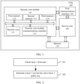
- FIG. 1 is a structural block diagram of a chip according to an embodiment of this application.
- the chip 100 includes a security core module 110, a service core 120, a memory 130, and a first communications interface 140.
- the chip 100 may further include components other than the foregoing components. These modules are not enumerated one by one herein. For ease of description, the following assumes that the chip 100 is a chip disposed in a server.
- the chip 100 may alternatively not include the service core 120.
- a function of the service core 120 may be provided by a chip configured in a same computing device as the chip 100 (specifically provided by a core that is inside the chip and that can run service firmware).
- a function of the service core 120 may be provided by a computing device that is jointly used with a computing device in which the chip 100 is configured (specifically provided by a core that is inside the computing device and that can run service firmware).
- the chip 100 may include a plurality of service cores or a plurality of memories. Different service cores may execute different service core firmware, to implement corresponding functions.
- the chip shown in FIG. 1 is a chip that imposes a relatively high requirement on security, for example, a BMC in a server, a system-on-a-chip (System-on-a-Chip, SoC) in a terminal device, or an SoC chip in a network device.
- SoC System-on-a-Chip
- the service core 120 may execute service core firmware, to implement corresponding functions of the chip.
- the service core 120 may execute the service core firmware, to implement functions that the BMC can implement, such as providing remote maintenance of the server, monitoring a running status of the server, obtaining running status information of a CPU, and other functions.
- the service core 120 may execute service core firmware, to implement functions that the SoC chip in the terminal device can implement, such as processing a communication protocol and communications data, controlling the entire terminal device, executing a software program, processing data of the software program, and other functions.
- the service core 120 may execute service core firmware, to implement functions that can be implemented by the SoC chip in the network device.
- the service core 120 may execute the service core firmware, to provide secure boot assurance for a baseband unit (baseband unit, BBU) (which may also be referred to as a digital unit (digital unit, DU)) when the BBU is started.
- BBU baseband unit
- DU digital unit
- the security core module 110 communicates with the memory 130 communicate through an internal connection path, to transfer a control and/or data signal.
- the service core 120 communicates with the memory 130 communicate through an internal connection path, to transfer a control and/or data signal.
- the memory 130 is a non-volatile memory that is writable and erasable for a plurality of times, for example, an electrically erasable programmable read-only memory (Electrically-Erasable Programmable Read-Only Memory, EEPROM) or a flash memory (Flash memory).
- EEPROM Electrically erasable programmable read-only memory
- flash memory Flash memory
- the security core module 110 includes a security core 111, a first memory 112, a second memory 113, a third memory 114, and a security core module communications interface 115.
- the security core 111 may communicate with the first memory 112, the second memory 113, and the third memory 114 through an internal connection path.
- the security core 111 may read information stored in the first memory 112, the second memory 113, and the third memory 114; or send information to the second memory 113 and the third memory 114, and the second memory 113 and the third memory 114 may store the received information.
- the security core 111 may also communicate with the security core module communications interface 115 through an internal connection path.
- the security core 111 may send information to another component, device, or apparatus through the security core module communications interface 115; or receive, through the security core module communications interface 115, information sent by another component, device, or apparatus.
- the security core module 110 may be connected to the service core 120 through an internal connection path.
- the security core 111 can access a component outside the security core module 110.
- the security core module 110 prevents external access. Specifically, the security core module 110 prevents access of an external module that is inside the chip 100 and that is other than the security core module 110, and the security core module 110 prevents access of an external device outside the chip 100.
- That the security core module 110 prevents access of an external module that is inside the chip 100 and that is other than the security core module 110 means that a module that is inside the chip 100 and that is other than the security core module 110 cannot access a component inside the security core module 110.
- the service core 120 cannot access the component inside the security core module 110.
- the service core 120 cannot access the first memory 112, the second memory 113, or the fourth memory 114 in the security core module 110.
- That the security core module 110 prevents access of an external device outside the chip 100 means that the external device outside the chip 100 cannot access the component inside the security core module 110.
- a CPU inside the server cannot access the component inside the security core module 110.
- the CPU inside the server cannot access the first memory 112, the second memory 113, or the fourth memory 114 in the security core module 110.
- the security core 111 can access the component outside the security core module 110.
- the security core 111 can access storage space of the service core 120, to obtain firmware run by the service core 120.
- the security core 111 can access the memory 130, to obtain data stored in the memory 130, or send, to the memory 130, data to be stored to the memory 130.
- the security core 111 can access a memory outside the chip 100, for example, a memory in the server, to obtain data stored in the memory, or send, to the memory, data desired to be stored to the memory.
- the security core module 110 prevents access of the service core 120.
- the service core 120 can access the component inside the security core module 110.
- the service core runs some limited code, and the code is verified secure code.
- the service core accesses the component inside the security core module 110, data stored in the security core module 110 is not tampered with, and the data stored in the security core module 110 is not leaked to an attacker. Therefore, accessing the component inside the security core module 110 by the service core when the service core is in the security mode is secure.
- the security core module 110 prevents access of the component outside the security core module 110 at any time. This can ensure that the service core 120 is completely isolated from the security core module 110, and avoid using the service core 120 to access the first memory 112, the second memory 113, and the third memory 114.
- the components (that is, the security core 111, the first memory 112, the second memory 113, the third memory 114, and the like) inside the security core module 110 include a master component, a slave component, and a master/slave component. All slave components are accessible by only a master component inside the security core, and are inaccessible by external components (that is, the external device and the external module). Addresses of the slave components inside the security core module 110 are beyond an address range that is accessible by the external components.
- the security core module communications interface 115 that is in the security core module 110 and that communicates with another component inside the chip 100 has only a master (master) interface, and has no slave (slave) interface. Therefore, the security core module 110 can externally initiate master access, but the component outside the security core module 110, such as the service core 120, cannot initiate master access to the component inside the security core module 110.
- an address of the component outside the security core module 110 is within the address space range that is accessible by the security core module 110, whereas addresses of the components (such as the security core 111 and the first memory 112) inside the security core module 110 are beyond an address space range that is accessible by the component outside the security core module 110.
- the security core module 110 may communicate with the component outside the security core module 110 through the security core module communications interface 115, whereas the component (such as the service core 120 or a component outside the chip 100) outside the security core module 110 cannot access the components inside the security core module 110, such as the memories in the security core module 110.
- the slave components inside the security core module 110 may be the memories in the security core module 110, such as the first memory 112, the second memory 113, and the third memory 114.
- the master component inside the security core module 110 may be the security core 111.
- the first memory 112 is configured to store a UDS of the chip 100.
- the UDS stored in the first memory 112 cannot be deleted or modified.
- the UDS stored in the first memory 112 cannot be deleted or modified at any time. If the UDS stored in the first memory 112 in the chip 100 is expected to be modified, the UDS can be modified only by using a new first memory.
- the UDS is used to generate a layer 1 private key and a layer 1 public key. In this case, if the UDS is tampered with, an error occurs on the layer 1 private key and the layer 1 public key. Therefore, that the UDS stored in the first memory 112 cannot be modified or deleted can improve security of the chip 100.
- the UDS stored in the first memory 112 is unalterable by making the UDS unalterable in a locking manner. In other words, the UDS stored in the first memory 112 is locked to make the UDS unalterable.
- each time after the chip 100 is powered on the UDS stored in the first memory 112 is allowed to be read only once.
- the UDS may be read to the third memory 114.
- the UDS is no longer read unless the chip 100 is reset.
- the UDS may be deleted from the third memory 114.
- the UDS is allowed to be read only once when the layer 1 public key and the layer 1 private key are generated. This can avoid that an attacker may forge the layer 1 private key and the layer 1 public key by using the UDS due to leakage of the UDS.
- the first memory 112 may be a one-time programmable non-volatile memory (One-time programmable non-volatile memory, OTP NVM).
- OTP NVM may also be referred to as a programmable read-only memory (Programmable read-only memory, PROM) or a one-time programmable (One-time programmable, OTP) memory.
- PROM programmable read-only memory
- OTP One-time programmable memory
- eFuse is a typical OTP memory.
- the OTP memory is a special type of non-volatile memory (NVM), and allows data to be written into the memory only once.
- the data written into the OTP memory may be disallowed to be deleted or modified by making the data unalterable in a locking manner.
- the UDS may be written into the first memory 112 in a chip manufacturing phase, and is made to be unalterable in a locking manner. In this way, the UDS written into the first memory 112 cannot be deleted or modified.
- the UDS may be a mutable random number written into the first memory 112 by using a hardware interface or a software interface in a device production process. Different devices have different UDSs. Therefore, the UDS is characterized by randomness.
- the device production process may be a process of fabricating the chip 100 on a circuit board.
- the UDS may be generated by a dedicated device by using a physical unclonable function (physical unclonable function, PUF) technology in a phase of producing the chip 100, and then written into the first memory 112.
- PUF physical unclonable function
- the first memory 112 is configured to store a UDS of the chip 100.
- the UDS stored in the first memory 112 cannot be deleted or modified in a working process of the chip 100.
- the first memory 112 may be a memory in which data stored in the first memory 112 can be deleted or modified only by using a specific device.
- the first memory 112 may be an erasable programmable read-only memory (Erasable Programmable Read Only Memory, EPROM).
- EPROM erasable programmable read-only memory
- a quartz window is included in an EPROM package, and data in the EPROM can be deleted by shining strong ultraviolet light through the quartz window. Usually, the quartz window of the EPROM into which the data is written is covered, to protect against direct sunlight. Therefore, the data in the EPROM cannot be deleted or modified in the working process of the chip 100.
- the first memory 112 may include a secure boot indicator bit.
- the secure boot indicator bit After writing of data in the first memory 112 is completed, the secure boot indicator bit is set to be enabled. For example, if a value of the secure boot indicator bit is 0, it indicates that the secure boot indicator bit is not enabled. In this case, writing of the data in the first memory 112 is not completed. If a value of the secure boot indicator bit is 1, it indicates that the secure boot indicator bit is enabled. In this case, writing of the data in the first memory 112 is completed.
- the first memory 112 may further store first check information.
- the first check information is related information used to check layer 1 firmware.
- the first check information may include a hash (hash) of a first root public key, first revocation identification information, and first security version number information.
- the first memory 112 may store only the hash of the first root public key.
- the first revocation identification information and/or the first security version number information may be stored in the second memory 113.
- all content in the first check information may be stored in the first memory 112.
- the hash of the first root public key that is stored in the first memory 112 is disallowed to be deleted and modified. Specifically, after being written into the first memory 112, the hash of the first root public key is made to be unalterable in a locking manner. In other words, the hash of the first root public key that is written into the first memory 112 is locked to make the hash of the first root public key unalterable. This can avoid that the layer 1 firmware cannot be checked because of modification of the hash of the first root public key.
- the hash of the first root public key that is stored in the first memory 112 is disallowed to be deleted or modified in the working process of the chip 100.
- the first revocation identification information can be modified.
- a modification manner is modifying 0 in the first revocation identification information to 1. However, 1 in the first revocation identification information cannot be modified to 0.
- 10 is a revocation identifier included in the first revocation identification information, and 10 can be modified to 11 but cannot be modified to 00 or 01.
- the first security version number can be modified.
- a modification manner is modifying 0 in the first security version number information to 1. However, 1 in the first security version number information cannot be modified to 0.
- 10 is a security version number included in the first security version number information, and 10 can be modified to 11 but cannot be modified to 00 or 01.
- the first check information may include only the hash of the first root public key.
- the first check information may include the hash of the first root public key, and the first check information may further include either the first revocation identification information or the first security version number information.
- the second memory 113 is configured to store boot (Boot-Rom) code.
- the second memory 113 is a non-volatile memory (non-volatile memory, NVM).
- NVM non-volatile memory
- the second memory 113 may be a read-only memory (read-only memory, ROM), or may be a PROM, an EPROM, an OTP NVM, an EEPROM, a flash memory, or the like.
- the third memory 114 may be a writable/readable memory, that is, a memory that is writable and erasable for a plurality of times.
- the third memory 114 may be a random-access memory (Random-Access Memory), such as a static random-access memory (Static Random-Access Memory, SRAM) or a dynamic random-access memory (Dynamic Random Access Memory, DRAM).
- the third memory may be a memory that is writable and erasable for a plurality of times, such as an EEPROM or a flash memory.
- the NVM includes an OTP NVM. Therefore, in some embodiments, the first memory 112 and the second memory 113 may be implemented by one memory.
- the memory may implement functions of the first memory 112 and the second memory 113. To be specific, the memory may be configured to store the UDS, the first check information, and the boot code.
- the function of the first memory 112 and the function of the second memory 113 may alternatively be implemented respectively by using two OTP NVMs.
- the second memory 113 and the third memory 114 may also be implemented by one memory.
- the memory is an NVM that is writable and erasable for a plurality of times.
- the memory may implement functions of the second memory 113 and the third memory 114.
- the memory may be configured to store the boot code and duplicate layer 1 firmware.
- the function of the second memory 113 and the function of the third memory 114 may alternatively be implemented respectively by using two NVMs that are writable and erasable for a plurality of times.
- the security core 111 may be configured to perform a method shown in FIG. 2 , to complete trusted identity construction for the layer 1 firmware.
- the security core 111 checks the layer 1 firmware.
- step 202 is performed.
- a process of checking the layer 1 firmware by the security core 111 refer to a flowchart shown in FIG. 3 .
- the security core 111 if the security core 111 fails in checking the layer 1 firmware, the security core 111 stops running, sends a check failure indication message, and informs a user that the security core 111 fails in checking the layer 1 firmware.
- the security core 111 may check backup layer 1 firmware. If the security core 111 successfully checks the backup layer 1 firmware, step 202 is performed. If the security core 111 still fails in checking the backup layer 1 firmware, the security core 111 stops running, sends a check failure indication message, and informs a user that the security core 111 fails in checking the layer 1 firmware.
- the security core 111 generates a layer 1 private key and a layer 1 public key.
- FIG. 3 is a schematic flowchart for checking layer 1 firmware according to an embodiment of this application.
- the security core 111 implements a process of checking the layer 1 firmware shown in FIG. 3 by executing the Boot-Rom code stored in the second memory 113.
- the security core 111 checks the layer 1 firmware based on first check information and layer 1 firmware check related information.
- the layer 1 firmware check related information includes a first root public key, a signature result of a secondary public key, the secondary public key, and a signature result of the layer 1 firmware and a layer 1 firmware version number.
- the layer 1 firmware check related information may further include any one or more of the following information: a secondary key identifier (ID) and the layer 1 firmware version number.
- a memory configured to store the layer 1 firmware and the layer 1 firmware check related information is not limited in this embodiment of this application.
- the layer 1 firmware and the layer 1 firmware check related information may be stored in the second memory 113.
- the layer 1 firmware and the layer 1 firmware check related information may be stored in a memory outside the security core module 110.
- the layer 1 firmware and the layer 1 firmware check related information may be stored in the memory 130.
- the layer 1 firmware and the layer 1 firmware check related information may be stored in a memory outside the chip 100, for example, a memory in a server.
- the security core 111 may copy the layer 1 firmware into the third memory 114.
- the security core 111 may directly read the layer 1 firmware from the third memory 114, without reading the layer 1 firmware from the memory outside the security core module 110.
- the security core 111 accesses the third memory 114 faster than accesses the memory outside the security core 110. Therefore, copying the layer 1 firmware into the third memory 114 can increase a speed of checking the layer 1 firmware.
- the security core 111 may also copy the layer 1 firmware check related information into the third memory 114, to increase the speed of checking the layer 1 firmware. In other words, the security core 111 checks the layer 1 firmware stored in the third memory 114.
- the security core 111 may copy the layer 1 firmware into the third memory 114 after successfully checking the layer 1 firmware. In other words, the security core 111 checks the layer 1 firmware stored in the memory outside the security core module 110.
- the security core 111 may determine locations, in the memory, of the layer 1 firmware check related information and the layer 1 firmware based on an information header.
- the information header may indicate an offset location, in the memory, of each piece of information in the layer 1 firmware check related information and a size of each piece of information.
- the information header may indicate an offset location, in the memory, of the first root public key and a size of the first root public key, and indicate an offset location, in the memory, of the signature result of the secondary public key and a size of the signature result of the secondary public key.
- the information header may further indicate an offset location, in the memory, of the layer 1 firmware and a size of the layer 1 firmware.
- the information header is merely used as an example for description, and the information header may alternatively indicate other content.
- a process of checking the layer 1 firmware by the security core 111 based on the first check information and the layer 1 firmware check related information is as follows:
- the first memory 112 includes a secure boot indicator bit
- a process of checking the first root public key in the layer 1 firmware related information by using the hash of the first root public key includes: calculating a hash of the first root public key, and comparing the calculated hash of the first root public key with the hash of the first root public key that is stored in the first memory 112, to determine whether the two hashes are the same. If the two hashes are the same, the first root public key is successfully checked, and step 302 is performed; or if the two hashes are different, the check fails. If the first memory 112 includes no secure boot indicator bit, the first root public key may be checked directly by using the hash of the first root public key that is stored in the first memory 112.
- step 302 is performed after the first root public key is successfully checked, it can be ensured that the first root public key used in step 302 is trustworthy.
- the to-be-checked signature result of the secondary public key is generated in the following manner: performing a hash operation on the secondary public key to obtain a hash of the secondary public key, and encrypting (that is, performing signature processing on) the hash of the secondary public key by using a first root private key, to obtain the signature result of the secondary public key.
- a process of performing the signature check on the signature result of the secondary public key by using the first root public key includes: decrypting the signature result of the secondary public key by using the first root public key, to obtain a hash; performing hash calculation on the secondary public key, to obtain another hash; and comparing the two hashes to determine whether the two hashes are the same, and if the two hashes are the same, the signature check on the signature result of the secondary public key succeeds, or if the two hashes are different, the check fails.
- step 303 Determine, based on the first revocation identification information stored in the first memory 112, whether the secondary key identifier (ID) in the layer 1 firmware check related information has been revoked, and if the secondary key identifier has not been revoked, perform step 304, or if the secondary key identifier has been revoked, the check fails.
- ID secondary key identifier
- the first revocation identification information may include the secondary key identifier that has been revoked. In this case, if the first revocation identification information does not include the secondary key identifier, it is determined that the secondary key identifier has not been revoked; or if the first revocation identification information includes the secondary key identifier, it is determined that the secondary key identifier has been revoked.
- the first revocation identification information may include the secondary key identifier that has not been revoked. In this case, if the first revocation identification information includes the secondary key identifier, it is determined that the secondary key identifier has not been revoked; or if the first revocation identification information does not include the secondary key identifier, it is determined that the secondary key identifier has been revoked.
- step 303 may not be performed.
- whether the secondary key identifier has been revoked does not need to be determined.
- the layer 1 firmware related information does not need to include the secondary key identifier, and correspondingly, the first check information does not need to include the first revocation identification information, either.
- step 304 may be directly performed after the signature check in step 302 succeeds.
- step 304 Perform a signature check on the signature result of the layer 1 firmware and the layer 1 firmware version number by using the secondary public key, and if the signature check succeeds, perform step 305, or if the check fails, return a check failure.
- the to-be-checked signature result of the layer 1 firmware and the layer 1 firmware version number may be generated in the following two manners.
- Manner 1 Performing a hash operation on the layer 1 firmware and the layer 1 firmware version number to obtain a hash; and encrypting (that is, performing signature processing on) the hash by using a secondary private key, to obtain the signature result of the layer 1 firmware and the layer 1 firmware version number.
- Manner 2 Performing a hash operation on the layer 1 firmware to obtain a hash of the layer 1 firmware; performing a hash operation on the hash of the layer 1 firmware and the layer 1 firmware version number to obtain a hash; and encrypting (that is, performing signature processing on) the hash by using a secondary private key, to obtain the signature result of the layer 1 firmware and the layer 1 firmware version number.
- a process of performing the signature check on the signature result of the layer 1 firmware and the layer 1 firmware version number by using the secondary public key includes: decrypting the signature result of the layer 1 firmware and the layer 1 firmware version number by using the secondary public key, to obtain a hash; performing a hash operation on the layer 1 firmware and the layer 1 firmware version number to obtain a hash; and comparing the two hashes to determine whether the two hashes are the same, and if the two hashes are the same, the signature check on the signature result of the layer 1 firmware and the layer 1 firmware version number succeeds, or if the two hashes are different, the check fails.
- a process of performing the signature check on the signature result of the layer 1 firmware and the layer 1 firmware version number by using the secondary public key includes: decrypting the signature result of the layer 1 firmware and the layer 1 firmware version number by using the secondary public key, to obtain a hash; performing a hash operation on the hash of the layer 1 firmware and the layer 1 firmware version number to obtain a hash; and comparing the two hashes to determine whether the two hashes are the same, and if the two hashes are the same, the signature check on the signature result of the layer 1 firmware and the layer 1 firmware version number succeeds, or if the two hashes are different, the check fails.
- step 305 Determine, based on the first security version number information stored in the first memory 112, whether the layer 1 firmware version number is a security version number, and if the layer 1 firmware version number is the security version number, perform step 306, or if the layer 1 firmware version number is not the security version number, the check fails.
- the first security version number information may include the security version number.
- the layer 1 firmware version number is the security version number; or if the first security version number information does not include the layer 1 firmware version number, the layer 1 firmware version number is not the security version number.
- the first security version number information may include a non-security version number. In this case, if the first security version number information does not include the layer 1 firmware version number, the layer 1 firmware version number is the security version number; or if the first security version number information includes the layer 1 firmware version number, the layer 1 firmware version number is not the security version number.
- step 305 may not be performed.
- whether the layer 1 firmware version number is the security version number does not need to be determined.
- the layer 1 firmware related information does not need to include the layer 1 firmware version number, and correspondingly, the first check information does not need to include the first security version number information, either.
- step 306 may be directly performed after the signature check in step 304 succeeds.
- the layer 1 firmware check related information should include a signature result of the layer 1 firmware instead of the signature result of the layer 1 firmware and the layer 1 firmware version number.
- an objected checked in step 304 is the signature result of the layer 1 firmware instead of the signature result of the layer 1 firmware and the layer 1 firmware version number.
- step 306. Perform hash calculation on the layer 1 firmware to obtain a hash of the layer 1 firmware; and compare the hash with the hash of the layer 1 firmware corresponding to the signature check that has been performed in step 304, and if the two hashes of the layer 1 firmware are the same, the check on the layer 1 firmware succeeds, or if the two hashes of the layer 1 firmware are different, the check fails.
- the security core 111 may perform a method shown in FIG. 4 , to generate a layer 1 private key and a layer 1 public key.
- FIG. 4 is a schematic flowchart for generating a layer 1 private key and a layer 1 public key according to an embodiment of this application.
- the security core 111 When successfully checking the layer 1 firmware based on the first check information, the security core 111 continues to execute the Boot-Rom code stored in the second memory 113, to generate a CDI.
- the security core 111 may determine the CDI based on a UDS and a hash of the layer 1 firmware, and transfer the CDI to the layer 1 firmware, so that the layer 1 firmware determines the layer 1 private key and public key based on the CDI.
- a manner of transferring the CDI may be storing the CDI to the third memory 114.
- the security core 111 may be configured to perform one-way calculation based on the UDS and the hash of the layer 1 firmware by using a one-way function, to generate the CDI.
- the one-way function for one-way calculation may be hashed message authentication code (Hash-based message authentication code, HMAC), the secure hash algorithm (Secure Hash Algorithms, SHA)-256, SHA-512, the MD5 message digest algorithm (MD5 Message-Digest Algorithm), or the like.
- the security core 111 may be configured to calculate HMAC(UDS, Hash(Layer1)) to generate the CDI, where UDS represents the UDS stored in the first memory 112, and Hash(Layer1) represents hashing of the layer 1 firmware.
- HMAC(UDS, Hash(Layer1)) means performing an HMAC signature on the hash of the layer 1 firmware by using the UDS as a key, and an obtained signature is the CDI.
- the security core 111 may run the layer 1 firmware to generate the layer 1 private key and the layer 1 public key, and store the generated layer 1 private key to the third memory 114, where the layer 1 public key may be stored in a memory outside the security core module 110 such as the memory 130, or may be stored in a memory outside the chip 100 such as a memory in a server.
- An asymmetric cryptographic algorithm used for generating the layer 1 public key and the layer 1 private key may be a Rivest-Shamir-Adleman (Rivest-Shamir-Adleman, RSA) cryptographic algorithm, such as RSA-2048, RSA-3072, or RSA-4096, or may be an elliptic curve cryptography (elliptic curve cryptography, ECC) algorithm, such as ECC 256, ECC 384, or ECC 512.
- Rivest-Shamir-Adleman Rivest-Shamir-Adleman
- RSA Rivest-Shamir-Adleman
- ECC elliptic curve cryptography
- each time after the chip 100 is powered on the UDS stored in the first memory 112 is allowed to be read only once.
- any other device outside the security core module 110 cannot access a component inside the security core module 110, or can access a component inside security core module 110 only when the service core 120 is in a security mode. In this way, the layer 1 private key stored in the third memory 114 cannot be leaked. This can avoid a risk of forging a layer 2 certificate by using the layer 1 private key.
- the security core 111 may further send layer 1 certificate information to a certificate authority device through the security core module communications interface 115; and receive, through the security core module communications interface 115, the layer 1 certificate information that is signed by using a CA private key (a CA signature layer 1 certificate for short below) and that is sent by the certificate authority device.
- a CA private key a CA signature layer 1 certificate for short below
- the layer 1 certificate information may be a variety of information including the layer 1 public key.
- the layer 1 certificate information may include an identity of the layer 1 firmware.
- the identity of the layer 1 firmware may be the hash of the layer 1 firmware.
- the layer 1 certificate information may be a layer 1 certificate generated by the security core 111.
- the layer 1 certificate includes the layer 1 public key.
- the layer 1 certificate may further include an identity of the layer 1 firmware, and the identity of the layer 1 firmware may be the hash of the layer 1 firmware.
- the layer 1 certificate information may be a self-signed certificate obtained after the security core 111 performs self-signature.
- the security core 111 may generate a layer 1 certificate, and sign the layer 1 certificate by using the layer 1 private key, to obtain the self-signed certificate. Therefore, the self-signed certificate includes the layer 1 public key.
- the self-signed certificate may further include an identity of the layer 1 firmware, and the identity of the layer 1 firmware may be the hash of the layer 1 firmware. Signing the layer 1 certificate by using the layer 1 private key can ensure integrity of the layer 1 certificate. To be specific, if some bytes in the layer 1 certificate are modified in a transfer process, the modifications may also be identified.
- the layer 1 certificate information may be a certificate signing request (certificate signing request, CSR), where the CSR includes a layer 1 certificate generated by the security core 111. Therefore, the CSR includes the layer 1 public key.
- the CSR may further include an identity of the layer 1 firmware, and the identity of the layer 1 firmware may be the hash of the layer 1 firmware.
- the CA signature layer 1 certificate includes the layer 1 public key. If the layer 1 certificate information further includes the identity of the layer 1 firmware, the CA signature layer 1 certificate may further include the identity of the layer 1 firmware.
- the security core 111 may perform the method shown in FIG. 2 , to generate the layer 1 private key and the layer 1 public key and generate the layer 1 certificate information based on the layer 1 public key.
- the chip 100 may be connected to the certificate authority device, to send the layer 1 certificate information to the certificate authority device.
- the certificate authority device sends the layer 1 certificate information to a CA center.
- the CA center signs the layer 1 certificate information by using the CA private key, to obtain the CA signature layer 1 certificate, and sends the CA signature layer 1 certificate to the certificate authority device; and the certificate authority device sends the received CA signature layer 1 certificate to the security core module 110 inside the chip 100.
- the security core module 110 may communicate with the first communications interface 140 through an internal connection path.
- the layer 1 certificate information may be directly sent to the certificate authority device through the first communications interface 140 of the chip 100.
- the security core 111 can access a component outside the security core module 110. Therefore, in some other embodiments, the layer 1 certificate information may be sent to the certificate authority device by using the service core 120. Specifically, the security core 111 may send the layer 1 certificate information to the service core 120 through the security core module communications interface 115, and the service core 120 may send the layer 1 certificate information to the certificate authority device through the first communications interface 140.
- the security core module 110 prevents access of the component outside the security core module 110
- the component outside the security core module 110 may send some information to the security core module 110. Therefore, in some embodiments, the CA signature layer 1 certificate that is sent by the certificate authority device and that is received by the first communications interface 140 may be directly sent to the security core module communications interface 115.
- the security core 111 obtains the CA signature layer 1 certificate received by the security core module communications interface 111.
- the first communications interface 140 may send the received CA signature layer 1 certificate to the service core 120.
- the service core 120 may write the received CA signature layer 1 certificate into specific storage space of the memory 130.
- the specific storage space is storage space shared by the service core 120 with the security core 111.
- both the service core 120 and the security core 111 can access the storage space, and read data stored in the storage space or write data into the storage space.
- the security core 111 may periodically access the specific storage space through the security core module communications interface 115. If determining that the storage space stores the CA signature layer 1 certificate, the security core 111 obtains the CA signature layer 1 certificate through the security core module communications interface 115.
- the service core 120 may send some indication information to the security core 111. Therefore, in some other embodiments, the first communications interface 140 may send the received CA signature layer 1 certificate to the service core 120.
- the service core 120 may write the received CA signature layer 1 certificate into the specific storage space of the memory 130, and then send indication information to the security core 111, where the indication information is used to instruct the security core 111 to read the specific storage space.
- the security core 111 reads the specific storage space through the security core module communications interface 115, to obtain the CA signature layer 1 certificate.
- the chip 100 may further include a second communications interface (not shown in the figure).
- the service core 120 may communicate with the second communications interface through an internal connection path, but the service core 120 cannot communicate with the first communications interface 140.
- the chip 100 may include two communications interfaces used for performing communication with a device outside the chip.
- the security core module 110 may communicate with the device outside the chip through one (for example, the first communications interface) of the two communications interface, and the service core 120 may communicate with the device outside the chip through the other communications interface (for example, the second communications interface).
- the security core 111 may send the CA signature layer 1 certificate to a memory through the security core communications interface 115.
- the memory stores the received CA signature layer 1 certificate.
- the memory is a non-volatile memory, for example, may be the memory 130; or may be a memory that is disposed outside the chip 100 in a process of producing the chip 100 and that can be accessed by the chip 100.
- the security core 111 may further delete the CDI stored in the third memory 114.
- the trusted identity of the layer 1 firmware is successfully constructed.
- the third memory 114 stores the layer 1 private key. The layer 1 private key may be applied to trusted certification.
- a process of obtaining the CA signature layer 1 certificate (including generating the layer 1 certificate information, sending the layer 1 certificate information to the certificate authority device, receiving the CA signature layer 1 certificate, and writing the CA signature layer 1 certificate into a memory) is implemented by running the layer 1 firmware.
- the layer 1 firmware may be further configured to check the layer 2 firmware, and generate a layer 2 private key, a layer 2 certificate, and a layer 2 public key.
- the security core 111 When successfully checking the layer 2 firmware, the security core 111 further determines layer 2 encryption information based on the CDI and a hash of the layer 2 firmware, and stores the layer 2 encryption information to the third memory 114.
- the security core 111 may calculate HMAC(CDI, Hash(Layer2)) to generate the layer 2 encryption information, where CDI may be the CDI stored in the third memory 114 or a value obtained by performing an operation on the CDI stored in the third memory 114 and other data, Hash(Layer2) represents hashing of the layer 2 firmware.
- HMAC(CDI, Hash(Layer2)) means performing an HMAC signature on the hash of the layer 2 firmware by using the CDI as a key, and an obtained signature is the layer 2 encryption information.
- the security core 111 further generates the layer 2 private key and the layer 2 public key based on the layer 2 encryption information by using an asymmetric cryptographic algorithm, and stores the layer 2 private key to the third memory 114; and issues the layer 2 certificate, and signs the layer 2 certificate by using the layer 1 private key.
- the layer 2 certificate includes the layer 2 public key and an identity of the layer 2 firmware, and the identity of the layer 2 firmware may be the hash of the layer 2 firmware.
- the hash of the layer 2 firmware may be obtained by performing a hash operation on the layer 2 firmware.
- the third memory 114 stores the layer 1 private key and the layer 2 private key.
- the layer 2 public key and the signed layer 2 certificate may be stored in a memory outside the security core module 110 such as the memory 130, or may be stored in a memory outside the chip 100 such as a memory in a server.
- any other device outside the security core module 110 cannot access a component inside the security core module 110, or can access a component inside security core module 110 only when the service core 120 is in a security mode. In this way, the layer 1 private key and the layer 2 private key that are stored in the third memory 114 cannot be leaked. This can avoid a risk of forging the layer 2 certificate by using the layer 1 private key and a risk of performing fake trusted certification by using the layer 2 private key.
- the layer 2 public key is used to verify the trusted certification, and therefore the layer 2 public key does not need to be kept confidential.
- the memory that stores the layer 2 public key may be the memory outside the security core module 110, so that another device obtains the layer 2 public key and performs verification by using the layer 2 public key.
- the asymmetric cryptographic algorithm used for generating the layer 2 public key and the layer 2 private key may be an RSA cryptographic algorithm, such as RSA-2048, RSA-3072, or RSA-4096, or may be an ECC algorithm, such as ECC 256, ECC 384, or ECC 512.
- an algorithm used for generating the layer 1 certificate may be the same as an algorithm used for generating the layer 2 certificate.
- an algorithm used for generating the layer 1 certificate may be different from an algorithm used for generating the layer 2 certificate.
- the asymmetric cryptographic algorithm used for generating the layer 2 public key and the layer 2 private key may be the same as the asymmetric cryptographic algorithm used for generating the layer 1 public key and the layer 1 private key.
- the asymmetric cryptographic algorithm used for generating the layer 2 public key and the layer 2 private key may alternatively be different from the asymmetric cryptographic algorithm used for generating the layer 1 public key and the layer 1 private key.
- the security core 111 may further delete the CDI stored in the third memory 114, after determining the layer 2 encryption information; and delete the layer 1 private key stored in the third memory 114, after signing the layer 2 certificate by using the layer 1 private key. This can avoid that an attacker may forge the layer 2 certificate based on the layer 1 private key due to leakage of the layer 1 private key and the CDI.
- the layer 1 firmware may be used to: generate the layer 1 certificate information, and transfer the layer 1 certificate information to the layer 2 firmware.
- the layer 2 firmware is used to: send the layer 1 certificate information to the certificate authority device, receive the CA signature layer 1 certificate, and write the CA signature layer 1 certificate into a memory.
- the security core module 110 stores the layer 1 private key, and the memory stores the CA signature layer 1 certificate.
- the security core 111 may provide, by running the layer 1 firmware, trusted certification for data on which trusted certification needs to be performed. Specifically, the security core 111 may obtain the layer 1 private key, and sign, by using the layer 1 private key, the data on which trusted certification needs to be performed, so as to provide trusted certification. In addition, the security core 111 may further provide trusted certification of the layer 1 firmware (that is, provide the CA signature layer 1 certificate).
- the security core module 110 stores the layer 2 private key, and the memory stores the CA signature layer 1 certificate and the layer 2 certificate that is signed by using the layer 1 private key.
- the security core 111 may provide, by running the layer 2 firmware, trusted certification for data on which trusted certification needs to be performed.
- the security core 111 may provide trusted certification of the layer 1 firmware (that is, provide the CA signature layer 1 certificate), and the security core 111 may further provide trusted certification of the layer 2 firmware (that is, provide the layer 2 certificate that is signed by using the layer 1 private key).
- the security core 111 may further sign, by using the layer 2 private key, the data on which trusted certification needs to be performed, so as to provide trusted certification.
- target data the data on which trusted certification needs to be performed.
- target data the data on which trusted certification needs to be performed.
- a type of the target data may include firmware (or code) run by hardware in a server, a hash of firmware (or code) running in the server, data generated in a running process of the server, and/or data stored in the server.
- the target data may be layer 1 firmware in security core firmware.
- the target data may alternatively be layer 2 firmware in security core firmware.
- the target data may alternatively be non-security core firmware or code, such as universal boot loader (Universal Boot Loader, U-Boot) code run by the service core inside the chip 100, operating system (Operating System, OS) kernel (kernel) firmware, or application (Application, APP) code running in an OS.
- the target data may alternatively be some data generated in a running process of a security core.
- the target data may alternatively be some data generated in a running process of other hardware in the server, for example, some data generated by a CPU inside the server.
- the target data may alternatively be some data stored in a memory in the server.
- the embodiment shown in FIG. 5 is described by using an example in which the security core firmware includes the layer 2 firmware.
- the embodiment shown in FIG. 5 is performed based on completion of trusted identity construction for the layer 2 firmware.
- FIG. 5 is a schematic diagram of a trusted certification process according to an embodiment of this application.
- the challenge device may be a device inside the server.
- the challenge device may be a central processing unit (Central Processing Unit, CPU) inside the server or a basic input/output system (Basic Input Output System, BIOS) inside the server.
- the challenge device may alternatively be a device that is outside the server and that can communicate with the server.
- the challenge device may be a terminal device that can access the server.
- the challenge device may be a device configured to verify whether the server is securely running.
- the verification request message may be used to request to obtain trusted certification of specific firmware.
- the verification request message may be used to request to obtain trusted certification of specific data.
- the specific data may be some critical data generated by a service core inside the chip 100.
- the specific data may be some critical data stored in a memory in the server.
- the specific data may be some critical data generated by a CPU inside the server.
- the server determines the trusted certification of the target data.
- the security core in the chip 100 in the server may be responsible for determining the trusted certification of the target data.
- the trusted certification of the layer 1 firmware in the security core firmware is the CA signature layer 1 certificate.
- the trusted certification of the layer 2 firmware in the security core firmware is the layer 2 certificate signed by using the layer 1 private key.
- the trusted certification of the target data is the firmware or a certificate of the firmware that is signed by using the layer 2 private key.
- the trusted certification of the target data is the specific data or a hash of the specific data that is signed by using the layer 2 private key.
- the server sends verification feedback information to the challenge device, where the verification feedback information includes the trusted certification of the target data.
- the challenge device may verify, based on stored verification data, whether the trusted certification of the target data is trustworthy.
- FIG. 7 is a structural block diagram of a chip according to an embodiment of this application. As shown in FIG. 7 , the chip 700 includes a security core module 710, and the security core module 710 includes a security core 711 and a memory 712.
- the memory 712 is configured to store a hash of a first root public key and a UDS of the chip.
- the security core 711 is configured to generate a layer 1 public key and a layer 1 private key based on the hash of the first root public key and the UDS of the chip.
- the memory 712 is configured to store the layer 1 private key.
- generating the layer 1 public key and the layer 1 private key by the security core 711 refer to the flowchart shown in FIG. 2 .
- the memory 712 refer to the descriptions about the first memory, the second memory, and the third memory in the chip shown in FIG. 1 . Details are not described herein again.
- the memory 712 is further configured to store a hash of a second root public key.
- the security core 711 is further configured to generate a layer 2 public key and a layer 2 private key based on the hash of the second root public key and the UDS.
- the memory 712 is further configured to store the layer 2 private key.
- the memory 712 is further configured to sign a layer 2 certificate by using the layer 1 private key, where the layer 2 certificate includes the layer 2 public key.
- generating the layer 2 public key and the layer 2 private key based on the hash of the second root public key and the UDS may be generating the layer 2 public key and the layer 2 private key based on the hash of the second root public key and a CDI that is generated by using the UDS.
- the second root public key may be the same as or different from the first root public key.
- the security core 711 is further configured to delete the layer 1 private key after signing the layer 2 certificate by using the layer 1 private key.
- the security core 711 is further configured to: run secure firmware when receiving verification request information that is specific to target data and that is sent by a challenge device, to sign the target data based on the layer 2 private key; and send the signed target data to the challenge device, so that the challenge device verifies the signed target data based on the layer 2 public key.
- the secure firmware herein is firmware used to implement a trusted certification process. Because the target data is signed by using the layer 2 private key in the trusted certification process, the secure firmware is layer 2 firmware.
- the security core is further configured to: run secure firmware when receiving verification request information that is specific to target data and that is sent by a challenge device, to sign the target data based on the layer 1 private key; and send the signed target data to the challenge device, so that the challenge device verifies the signed target data based on the layer 1 public key.
- the secure firmware herein is firmware used to implement a trusted certification process. Because the target data is signed by using the layer 1 private key in the trusted certification process, the secure firmware may be layer 1 firmware. Certainly, if the security core 711 does not delete the layer 1 private key after signing the layer 2 certificate by using the layer 1 private key, the trusted certification process may alternatively be implemented by layer 2 firmware.
- the chip further includes a service core (not shown in the figure), configured to run service firmware.
- the chip further includes a first input/output interface and a second input/output interface (which are not shown in the figure), the first input/output interface is coupled to the security core module, and the second input/output interface is coupled to the service core.
- a server serves as a target device in which the chip is disposed is used as an example for description. It can be understood that the chip shown in FIG. 1 or FIG. 7 may be applied to various computer devices, such as a server (for example, a storage server, a database server, or a management server), a terminal device (for example, a mobile terminal or a personal computer), a wearable device, and a network device (for example, a router or a switch).
- a server for example, a storage server, a database server, or a management server
- a terminal device for example, a mobile terminal or a personal computer
- a wearable device for example, a wearable device
- a network device for example, a router or a switch
- FIG. 8 is a schematic structural diagram of a server according to this application.
- the server 800 includes a processor 810 and a baseboard management controller (baseboard management controller, BMC) 820.
- the BMC 820 may be a security chip
- the security chip may be the chip 100 shown in FIG. 1 or the chip 700 shown in FIG. 7
- the processor 810 may be, for example, a CPU.
- the BMC 820 may perform the process shown in FIG. 2 , to complete trusted identity construction for layer 1 firmware or further complete trusted identity construction for layer 2 firmware.
- the BMC 820 may be further connected to other components, for example, connected to a 4th generation double data rate (double data rate, DDR) memory (DDR4 for short), a register, a BMC flash memory, a video interface, and a physical layer chip (for example, a network adapter).
- DDR double data rate
- the DDR4 is configured to provide program or code running space for the BMC 820 or the processor 810.
- the BMC flash memory may be a flash memory that stores firmware in the BMC and related data.
- the video interface is configured to connect to an external device such as a display.
- the physical layer chip is connected to the network adapter, and is configured to provide data receiving and sending services for the server 800.
- Both the BMC 820 and the processor 810 may access a BIOS by using a switch and run the BIOS stored in a BIOS flash memory.
- the processor 810 communicates with the BMC 820 by switching the switch.
- An architecture of the server 800 is merely an example for description, and shall not be construed as any limitation on application of the technical solutions provided in this application.
- the technical solutions provided in this application may be further applied to a server including more or fewer components.
- the server 800 may be a cloud computing server.
- the server 800 may include a plurality of computing units.
- the computing units may be CPUs, graphics processing units (graphics processing unit, GPU), digital signal processors (digital signal processor, DSP), application-specific integrated circuits (application specific integrated circuit, ASIC), field programmable gate arrays (field programmable gate array, FPGA), neural-network processing units (neural-network process unit, NPU), or other types of computing units.
- the plurality of computing units may constitute a homogenous computing (homogenous computing) resource pool and/or a heterogeneous computing (heterogeneous computing) resource pool, to provide services for a user.
- the server 800 may be a storage server.
- the server 800 may include a plurality of storage units.
- the storage units may be hard disk drives (hard disk drive, HDD), solid state disks (solid state disk, SSD), small computer system interface (small computer system interface, SCSI) disks, or other types of non-volatile storage media.
- the server 800 includes a plurality of hard disks, the plurality of hard disks may constitute a disk array (redundant arrays of independent drives, RAID) used as a storage resource pool of the server 800, to provide services for a user.
- RAID redundant arrays of independent drives
- FIG. 9 is a schematic structural diagram of a terminal device according to this application.
- the terminal device may be referred to as an access terminal, user equipment (user equipment, UE), a subscriber unit, a subscriber station, a mobile station, a mobile console, a remote station, a remote terminal, a mobile device, a user terminal, a terminal, a wireless communications device, a user agent, or a user apparatus.
- the access terminal may be a cellular phone, a handheld device having a wireless communication function, a computing device, another processing device connected to a wireless modem, a vehicle-mounted device, a wearable device, or a user device in a 5G communications system.
- the foregoing electronic devices are merely used as examples for describing the terminal device.
- the terminal device may alternatively be another electronic device, for example, a car or unmanned aerial vehicle including an SoC chip 901.
- the SoC chip 901 may be the chip 100 shown in FIG. 1 or the chip 700 shown in FIG. 7 .
- the mobile phone 900 when the terminal device is a mobile phone, the mobile phone 900 includes a security chip 901, a flash memory 902, a control circuit, an antenna, and an input/output apparatus.
- the SoC chip 901 is mainly configured to: process a communication protocol and communications data, and control the entire terminal device, execute a software program, and process data of the software program.
- the flash memory 902 is mainly configured to store the software program and data.
- the SoC chip 901 and the flash memory 902 are configured to provide secure boot assurance for the mobile phone 900 when the mobile phone 900 is powered on.
- the control circuit is mainly configured to convert between a baseband signal and a radio frequency signal and process a radio frequency signal.
- the control circuit together with the antenna may alternatively be referred to as a transceiver, which is mainly configured to receive and send radio frequency signals in an electromagnetic wave form.
- the input/output apparatus such as a touchscreen, a display screen, or a keyboard is mainly configured to receive data entered by a user and output the data to the user.
- the network device may be a base transceiver station (base transceiver station, BTS) in a code division multiple access (code division multiple access, CDMA) system, a NodeB (node B, NB) in a wideband code division multiple access (wideband code division multiple access, WCDMA) system, an evolved NodeB (evolutional node B, eNB) in a long term evolution (long term evolution, LTE) system, or a gNB (gNB) in a 5G communications system.
- the foregoing base stations are merely examples for description.
- the network device may be a relay node, an access point, a vehicle-mounted device, a wearable device, or a car or unmanned aerial vehicle including a security chip 1003.
- the BBU 1002 is mainly configured to perform baseband processing, control the base station 1000, and the like.
- An SoC chip 1003 and a flash memory 1004 are integrated into a board in the BBU 1002.
- the SoC chip 1003 may be the chip 100 shown in FIG. 1 or the chip 700 shown in FIG. 7 .
- the disclosed systems, apparatuses, and methods may be implemented in other manners.
- the described apparatus embodiments are merely examples.
- the unit division is merely logical function division and may be other division during actual implementation.
- a plurality of units or components may be combined or integrated into another system, or some features may be ignored or may not be performed.
- the displayed or discussed mutual couplings or direct couplings or communication connections may be implemented through some interfaces.
- the indirect couplings or communication connections between the apparatuses or units may be implemented in electrical, mechanical, or other forms.
- the units described as separate parts may or may not be physically separate, and parts displayed as units may or may not be physical units, may be located in one position, or may be distributed on a plurality of network units. Some or all of the units may be selected depending on an actual requirement, to achieve the objectives of the solutions in the embodiments.
- Embodiment 1 A chip, wherein the chip comprises a security core module, the security core module comprises a security core and a memory, the security core module prevents access of an external module that is inside the chip and that is other than the security core module, and the security core module prevents access of an external device outside the chip;
- Embodiment 2 The chip according to embodiment 1, wherein an address of the security core module is beyond an address range that is accessible by the external module and the external device.
- Embodiment 3 The chip according to embodiment 1 or 2, wherein the memory is further configured to store a hash of a second root public key;
- Embodiment 4 The chip according to embodiment 3, wherein the security core is further configured to delete the layer 1 private key after signing the layer 2 certificate by using the layer 1 private key.
- Embodiment 5 The chip according to embodiment 3 or 4, wherein the security core is further configured to: run secure firmware when receiving verification request information that is specific to target data and that is sent by a challenge device, to sign the target data based on the layer 2 private key; and send the signed target data to the challenge device, so that the challenge device verifies the signed target data based on the layer 2 public key.
- Embodiment 6 The chip according to any one of embodiments 1 to 3, wherein the security core is further configured to: run secure firmware when receiving verification request information that is specific to target data and that is sent by a challenge device, to sign the target data based on the layer 1 private key; and send the signed target data to the challenge device, so that the challenge device verifies the signed target data based on the layer 1 public key.
- Embodiment 7 The chip according to any one of embodiments 1 to 6, wherein the chip further comprises a service core, configured to run service core firmware.
- Embodiment 8 The chip according to embodiment 7, wherein the chip further comprises a first input/output interface and a second input/output interface, the first input/output interface is coupled to the security core module, and the second input/output interface is coupled to the service core.
- Embodiment 9 A private key generation method, wherein the method is performed by a security core in a chip; the security core is located in a security core module inside the chip, the security core module further comprises a memory configured to store a hash of a first root public key and a unique device secret UDS of the chip, the security core module prevents access of an external module that is inside the chip and that is other than the security core module, and the security core module prevents access of an external device outside the chip; and the method comprises:
- Embodiment 10 The method according to embodiment 9, wherein the memory is further configured to store a hash of a second root public key, and the method further comprises:
- Embodiment 11 The method according to embodiment 10, wherein the method further comprises: deleting, by the security core, the layer 1 private key after signing the layer 2 certificate by using the layer 1 private key.
- Embodiment 12 The method according to embodiment 10 or 11, wherein the method further comprises:
- Embodiment 13 The method according to embodiment 9 or 10, wherein the method further comprises: obtaining, by the security core, verification request information that is specific to target data and that is sent by a challenge device;
- Embodiment 14 A trusted certification method, wherein the method comprises:
- Embodiment 15 The method according to embodiment 14, wherein the obtaining, by a security core in a security core module inside a chip, verification request information sent by a challenge device comprises: reading, by the security core, the verification request information stored in specific storage space of the memory in the chip.
- Embodiment 16 The method according to embodiment 15, wherein before the reading, by the security core, the verification request information stored in the memory in the chip, the method further comprises: receiving, by the security core, indication information sent by a service core inside the chip, wherein the indication information is used to instruct the security core to read the specific storage space of the memory in the chip.
Landscapes
- Engineering & Computer Science (AREA)
- Computer Security & Cryptography (AREA)
- Computer Networks & Wireless Communication (AREA)
- Signal Processing (AREA)
- Theoretical Computer Science (AREA)
- Computer Hardware Design (AREA)
- General Engineering & Computer Science (AREA)
- Software Systems (AREA)
- Physics & Mathematics (AREA)
- General Physics & Mathematics (AREA)
- Mathematical Physics (AREA)
- Power Engineering (AREA)
- Storage Device Security (AREA)
Priority Applications (1)
| Application Number | Priority Date | Filing Date | Title |
|---|---|---|---|
| EP24220444.4A EP4546175A3 (de) | 2018-10-09 | 2018-10-09 | Chip, verfahren zur erzeugung privater schlüssel und vertrauenswürdiges zertifizierungsverfahren |
Applications Claiming Priority (3)
| Application Number | Priority Date | Filing Date | Title |
|---|---|---|---|
| EP24220444.4A EP4546175A3 (de) | 2018-10-09 | 2018-10-09 | Chip, verfahren zur erzeugung privater schlüssel und vertrauenswürdiges zertifizierungsverfahren |
| PCT/CN2018/109537 WO2020073206A1 (zh) | 2018-10-09 | 2018-10-09 | 芯片、生成私钥的方法和可信证明的方法 |
| EP18936726.1A EP3809625B1 (de) | 2018-10-09 | 2018-10-09 | Chip, verfahren zur erzeugung eines privaten schlüssels und verfahren zur vertrauenswürdigen verifizierung |
Related Parent Applications (1)
| Application Number | Title | Priority Date | Filing Date |
|---|---|---|---|
| EP18936726.1A Division EP3809625B1 (de) | 2018-10-09 | 2018-10-09 | Chip, verfahren zur erzeugung eines privaten schlüssels und verfahren zur vertrauenswürdigen verifizierung |
Publications (2)
| Publication Number | Publication Date |
|---|---|
| EP4546175A2 true EP4546175A2 (de) | 2025-04-30 |
| EP4546175A3 EP4546175A3 (de) | 2025-06-18 |
Family
ID=70164436
Family Applications (2)
| Application Number | Title | Priority Date | Filing Date |
|---|---|---|---|
| EP24220444.4A Pending EP4546175A3 (de) | 2018-10-09 | 2018-10-09 | Chip, verfahren zur erzeugung privater schlüssel und vertrauenswürdiges zertifizierungsverfahren |
| EP18936726.1A Active EP3809625B1 (de) | 2018-10-09 | 2018-10-09 | Chip, verfahren zur erzeugung eines privaten schlüssels und verfahren zur vertrauenswürdigen verifizierung |
Family Applications After (1)
| Application Number | Title | Priority Date | Filing Date |
|---|---|---|---|
| EP18936726.1A Active EP3809625B1 (de) | 2018-10-09 | 2018-10-09 | Chip, verfahren zur erzeugung eines privaten schlüssels und verfahren zur vertrauenswürdigen verifizierung |
Country Status (4)
| Country | Link |
|---|---|
| US (3) | US11722300B2 (de) |
| EP (2) | EP4546175A3 (de) |
| CN (1) | CN111264044B (de) |
| WO (1) | WO2020073206A1 (de) |
Families Citing this family (27)
| Publication number | Priority date | Publication date | Assignee | Title |
|---|---|---|---|---|
| EP3656577A1 (de) * | 2018-11-21 | 2020-05-27 | Thales Dis France SA | Reparatur eines betriebssystems vor ort unter verwendung einer erweiterung eines digitalen zertifikats |
| US11128474B2 (en) * | 2019-03-25 | 2021-09-21 | Micron Technology, Inc. | Secure device communication |
| CN114095172A (zh) * | 2020-07-02 | 2022-02-25 | 中国移动通信集团设计院有限公司 | 无线接口前传数据校验方法及装置 |
| CN111917756B (zh) * | 2020-07-27 | 2022-05-27 | 杭州叙简科技股份有限公司 | 一种执法记录仪基于公钥路由的加密系统及加密方法 |
| CN114003915B (zh) * | 2020-07-28 | 2025-10-31 | 华为技术有限公司 | 基于芯片的安全启动方法及装置 |
| CN112367165A (zh) * | 2020-10-19 | 2021-02-12 | 珠海格力电器股份有限公司 | 串口通信方法、装置、电子设备和计算机可读介质 |
| CN112417422B (zh) * | 2020-11-23 | 2024-06-18 | 深圳市中易通安全芯科技有限公司 | 安全芯片升级方法及计算机可读存储介质 |
| GB202020059D0 (en) * | 2020-12-17 | 2021-02-03 | Microsoft Technology Licensing Llc | Attesting update of a firmware layer |
| US12457103B2 (en) * | 2021-01-15 | 2025-10-28 | Micron Technology, Inc. | Server system to control memory devices over computer networks |
| US11522723B2 (en) * | 2021-03-01 | 2022-12-06 | Hewlett Packard Enterprise Development Lp | Secure provisiong of baseboard management controller identity of a platform |
| CN114640461B (zh) * | 2022-02-16 | 2024-11-05 | 深圳市优博讯科技股份有限公司 | 基于安全芯片的固件防篡改方法及系统 |
| CN116702148A (zh) * | 2022-02-28 | 2023-09-05 | 华为技术有限公司 | 一种可信计算方法、芯片以及服务器 |
| EP4479868A1 (de) * | 2022-03-22 | 2024-12-25 | Google LLC | Computersysteme mit zentralisierter beglaubigungsvorrichtung |
| CN115935335B (zh) * | 2022-10-14 | 2025-09-16 | 超聚变数字技术有限公司 | 一种固件的启动方法、芯片及计算设备 |
| US12216765B2 (en) * | 2022-10-26 | 2025-02-04 | Dell Products L.P. | Identity-based verification of software code layers |
| CN115688120B (zh) * | 2022-11-01 | 2026-08-11 | 杭州菲数科技有限公司 | 安全芯片固件导入方法、安全芯片及计算机可读存储介质 |
| CN115934592B (zh) * | 2023-01-20 | 2026-06-16 | 北京奕斯伟计算技术股份有限公司 | 一种数据处理装置和访存请求的处理方法 |
| CN116567624B (zh) * | 2023-07-10 | 2023-09-29 | 南京邮电大学 | 一种5g馈线终端通信安全防护方法、装置及存储介质 |
| KR20250026670A (ko) * | 2023-08-17 | 2025-02-25 | 삼성전자주식회사 | 펌웨어 업데이트 방법 및 장치 |
| KR20250050608A (ko) | 2023-10-06 | 2025-04-15 | 삼성전자주식회사 | 전자 장치의 식별자 생성 시스템 및 그것의 동작 방법 |
| CN117472465A (zh) * | 2023-10-26 | 2024-01-30 | 深圳市紫光同创电子有限公司 | 一种片上系统安全启动方法、装置、电子设备及存储介质 |
| EP4793803A1 (de) * | 2023-11-14 | 2026-08-19 | Huawei Technologies Co., Ltd. | Verfahren und vorrichtung zum schutz vor bmc-eindringung sowie bmc und computervorrichtung |
| CN118260768B (zh) * | 2024-04-11 | 2026-03-20 | 河南昆仑技术有限公司 | Bmc启动、bmc固件编译、bmc固件升级方法、芯片及计算设备 |
| CN118133326B (zh) * | 2024-05-07 | 2024-07-05 | 沐曦科技(北京)有限公司 | 一种基于芯片的数据加密传输系统 |
| CN121456921A (zh) * | 2024-07-31 | 2026-02-03 | 华为技术有限公司 | 一种设备信息保护方法及相关装置 |
| CN119808083B (zh) * | 2024-11-14 | 2025-08-01 | 成都芯盛集成电路有限公司 | 一种基于权限管理的rsic-v cpu安全芯片 |
| CN119210895B (zh) * | 2024-11-25 | 2025-02-25 | 中核控制系统工程有限公司 | 一种基于fpga和soc的可信通信方法 |
Family Cites Families (21)
| Publication number | Priority date | Publication date | Assignee | Title |
|---|---|---|---|---|
| US6760441B1 (en) * | 2000-03-31 | 2004-07-06 | Intel Corporation | Generating a key hieararchy for use in an isolated execution environment |
| CN100447763C (zh) * | 2003-05-29 | 2008-12-31 | 联想(北京)有限公司 | 一种安全芯片及基于该芯片的信息安全处理设备和方法 |
| JPWO2008117556A1 (ja) * | 2007-03-28 | 2010-07-15 | 日本電気株式会社 | ログ取得システム、ログ収集端末、ログ取得端末、それらを用いたログ取得方法及びプログラム |
| US8423789B1 (en) * | 2007-05-22 | 2013-04-16 | Marvell International Ltd. | Key generation techniques |
| CN101430747B (zh) * | 2008-09-26 | 2011-09-07 | 武汉大学 | 基于可信嵌入式平台的移动设备及其安全存储方法 |
| US20110154501A1 (en) * | 2009-12-23 | 2011-06-23 | Banginwar Rajesh P | Hardware attestation techniques |
| KR20140140552A (ko) * | 2012-03-19 | 2014-12-09 | 로얄 캐네디언 민트 | 자산 보관 및 이체 시스템에서의 외부 로그 저장소 |
| CN103514414A (zh) * | 2012-06-26 | 2014-01-15 | 上海盛轩网络科技有限公司 | 一种基于ARM TrustZone的加密方法及加密系统 |
| WO2014055148A2 (en) * | 2012-07-09 | 2014-04-10 | Massachusetts Institute Of Technology | Cryptography and key management device and architecture |
| GB2520489A (en) * | 2013-11-20 | 2015-05-27 | Ibm | Deletion of content in digital storage systems |
| US10148761B2 (en) * | 2015-04-09 | 2018-12-04 | Web Sensing, Llc | System-on-chip data security appliance and methods of operating the same |
| US20170277898A1 (en) * | 2016-03-25 | 2017-09-28 | Advanced Micro Devices, Inc. | Key management for secure memory address spaces |
| US20190199735A1 (en) * | 2016-06-29 | 2019-06-27 | Western Digital Technologies, Inc. | Device and method for verifying integrity of firmware |
| KR101795457B1 (ko) * | 2016-09-27 | 2017-11-10 | 시큐리티플랫폼 주식회사 | 보안 기능이 강화된 디바이스의 초기화 방법 및 디바이스의 펌웨어 업데이트 방법 |
| US20180198620A1 (en) * | 2017-01-11 | 2018-07-12 | Raptor Engineering, LLC | Systems and methods for assuring data on leased computing resources |
| CN108429719B (zh) * | 2017-02-14 | 2020-12-01 | 华为技术有限公司 | 密钥保护方法及装置 |
| CN108460282A (zh) * | 2017-02-22 | 2018-08-28 | 北京大学 | 一种基于异构多核芯片的计算机安全启动方法 |
| US11429592B2 (en) * | 2017-04-26 | 2022-08-30 | Visa International Service Association | Systems and methods for recording data representing multiple interactions |
| CN107908574B (zh) * | 2017-11-22 | 2021-09-10 | 深圳华中科技大学研究院 | 固态盘数据存储的安全保护方法 |
| DE102018208066A1 (de) * | 2018-05-23 | 2019-11-28 | Robert Bosch Gmbh | Datenverarbeitungseinrichtung und Betriebsverfahren hierfür |
| US10797421B2 (en) * | 2018-05-23 | 2020-10-06 | Xerox Corporation | Landing electrical contact |
-
2018
- 2018-10-09 CN CN201880064343.0A patent/CN111264044B/zh active Active
- 2018-10-09 WO PCT/CN2018/109537 patent/WO2020073206A1/zh not_active Ceased
- 2018-10-09 EP EP24220444.4A patent/EP4546175A3/de active Pending
- 2018-10-09 EP EP18936726.1A patent/EP3809625B1/de active Active
-
2021
- 2021-02-22 US US17/181,841 patent/US11722300B2/en active Active
-
2023
- 2023-06-19 US US18/337,062 patent/US12592821B2/en active Active
-
2026
- 2026-03-03 US US19/555,741 patent/US20260197169A1/en active Pending
Also Published As
| Publication number | Publication date |
|---|---|
| WO2020073206A1 (zh) | 2020-04-16 |
| CN111264044A (zh) | 2020-06-09 |
| CN111264044B (zh) | 2021-11-19 |
| US11722300B2 (en) | 2023-08-08 |
| EP3809625A4 (de) | 2021-09-08 |
| EP3809625A1 (de) | 2021-04-21 |
| US12592821B2 (en) | 2026-03-31 |
| US20230403151A1 (en) | 2023-12-14 |
| EP3809625B1 (de) | 2025-01-01 |
| EP4546175A3 (de) | 2025-06-18 |
| US20260197169A1 (en) | 2026-07-09 |
| US20210176056A1 (en) | 2021-06-10 |
Similar Documents
| Publication | Publication Date | Title |
|---|---|---|
| US12592821B2 (en) | Chip, private key generation method, and trusted certification method | |
| US20220292203A1 (en) | Technologies for device attestation | |
| US12348567B2 (en) | Attestation service for enforcing payload security policies in a data center | |
| JP7416775B2 (ja) | 周辺デバイス | |
| US20250211452A1 (en) | System and methods for confidential computing | |
| US11621843B2 (en) | Trusted remote proving method, apparatus and system | |
| CN109492352B (zh) | 一种设备标识组合引擎的实现方法及装置 | |
| EP3497878B1 (de) | Vorrichtung und verfahren zur verteilten zertifikatsregistrierung | |
| CN113656806A (zh) | 区块链一体机的可信启动方法及装置 | |
| US12524579B2 (en) | SRAM physically unclonable function (PUF) memory for generating keys based on device owner | |
| US12373518B2 (en) | Managing ownership of an electronic device | |
| EP3982609B1 (de) | Fernbeglaubigungsverfahren und -vorrichtung | |
| CN106610863A (zh) | 虚拟机可信迁移方法及装置 | |
| US20240152620A1 (en) | Owner revocation emulation container | |
| CN116680687A (zh) | 数据处理方法、装置、设备和存储介质 | |
| US11997192B2 (en) | Technologies for establishing device locality | |
| CN112000935A (zh) | 远程认证方法、装置、系统、存储介质及计算机设备 | |
| CN118591803A (zh) | 使用经授权子密钥进行安全启动的装置和方法 | |
| US20240249002A1 (en) | Storage system including storage device and host provisioning certificate into the storage device, system including the storage system, and method of operating the system | |
| WO2020199177A1 (zh) | 运行智能合约的方法和装置 | |
| CN116226872A (zh) | 安全启动方法、装置及相关器件 | |
| JP2024500822A (ja) | 鍵インストール方法、システム、装置、機器及びコンピュータプログラム | |
| US20250322041A1 (en) | Managing ownership of an electronic device | |
| CN120780367A (zh) | 一种bmc配置管理方法、装置、计算机设备及可读存储介质 |
Legal Events
| Date | Code | Title | Description |
|---|---|---|---|
| PUAI | Public reference made under article 153(3) epc to a published international application that has entered the european phase |
Free format text: ORIGINAL CODE: 0009012 |
|
| STAA | Information on the status of an ep patent application or granted ep patent |
Free format text: STATUS: THE APPLICATION HAS BEEN PUBLISHED |
|
| AC | Divisional application: reference to earlier application |
Ref document number: 3809625 Country of ref document: EP Kind code of ref document: P |
|
| AK | Designated contracting states |
Kind code of ref document: A2 Designated state(s): AL AT BE BG CH CY CZ DE DK EE ES FI FR GB GR HR HU IE IS IT LI LT LU LV MC MK MT NL NO PL PT RO RS SE SI SK SM TR |
|
| REG | Reference to a national code |
Ref country code: DE Ref legal event code: R079 Free format text: PREVIOUS MAIN CLASS: G06F0021000000 Ipc: H04L0009000000 |
|
| PUAL | Search report despatched |
Free format text: ORIGINAL CODE: 0009013 |
|
| AK | Designated contracting states |
Kind code of ref document: A3 Designated state(s): AL AT BE BG CH CY CZ DE DK EE ES FI FR GB GR HR HU IE IS IT LI LT LU LV MC MK MT NL NO PL PT RO RS SE SI SK SM TR |
|
| RIC1 | Information provided on ipc code assigned before grant |
Ipc: H04L 9/32 20060101ALI20250513BHEP Ipc: H04L 9/08 20060101ALI20250513BHEP Ipc: G06F 21/00 20130101ALI20250513BHEP Ipc: H04L 9/00 20220101AFI20250513BHEP |
|
| STAA | Information on the status of an ep patent application or granted ep patent |
Free format text: STATUS: REQUEST FOR EXAMINATION WAS MADE |
|
| 17P | Request for examination filed |
Effective date: 20251218 |