EP4546375A2 - Elément de filtre d'énergie pour implanteur ionique utilisé dans la production de plaquettes - Google Patents
Elément de filtre d'énergie pour implanteur ionique utilisé dans la production de plaquettes Download PDFInfo
- Publication number
- EP4546375A2 EP4546375A2 EP25163764.1A EP25163764A EP4546375A2 EP 4546375 A2 EP4546375 A2 EP 4546375A2 EP 25163764 A EP25163764 A EP 25163764A EP 4546375 A2 EP4546375 A2 EP 4546375A2
- Authority
- EP
- European Patent Office
- Prior art keywords
- filter
- energy
- substrate
- implantation
- ion
- Prior art date
- Legal status (The legal status is an assumption and is not a legal conclusion. Google has not performed a legal analysis and makes no representation as to the accuracy of the status listed.)
- Pending
Links
Images












Classifications
-
- H—ELECTRICITY
- H01—ELECTRIC ELEMENTS
- H01J—ELECTRIC DISCHARGE TUBES OR DISCHARGE LAMPS
- H01J37/00—Discharge tubes with provision for introducing objects or material to be exposed to the discharge, e.g. for the purpose of examination or processing thereof
- H01J37/02—Details
- H01J37/04—Arrangements of electrodes and associated parts for generating or controlling the discharge, e.g. electron-optical arrangement or ion-optical arrangement
- H01J37/05—Electron or ion-optical arrangements for separating electrons or ions according to their energy or mass
-
- G—PHYSICS
- G21—NUCLEAR PHYSICS; NUCLEAR ENGINEERING
- G21K—HANDLING OF PARTICLES OR IONISING RADIATION NOT OTHERWISE PROVIDED FOR; IRRADIATION DEVICES; GAMMA RAY OR X-RAY MICROSCOPES
- G21K1/00—Arrangements for handling particles or ionising radiation, e.g. focusing or moderating
- G21K1/02—Arrangements for handling particles or ionising radiation, e.g. focusing or moderating using diaphragms, collimators
- G21K1/025—Arrangements for handling particles or ionising radiation, e.g. focusing or moderating using diaphragms, collimators using multiple collimators, e.g. Bucky screens; other devices for eliminating undesired or dispersed radiation
-
- G—PHYSICS
- G21—NUCLEAR PHYSICS; NUCLEAR ENGINEERING
- G21K—HANDLING OF PARTICLES OR IONISING RADIATION NOT OTHERWISE PROVIDED FOR; IRRADIATION DEVICES; GAMMA RAY OR X-RAY MICROSCOPES
- G21K1/00—Arrangements for handling particles or ionising radiation, e.g. focusing or moderating
- G21K1/10—Scattering devices; Absorbing devices; Ionising radiation filters
-
- H—ELECTRICITY
- H01—ELECTRIC ELEMENTS
- H01J—ELECTRIC DISCHARGE TUBES OR DISCHARGE LAMPS
- H01J37/00—Discharge tubes with provision for introducing objects or material to be exposed to the discharge, e.g. for the purpose of examination or processing thereof
- H01J37/02—Details
- H01J37/04—Arrangements of electrodes and associated parts for generating or controlling the discharge, e.g. electron-optical arrangement or ion-optical arrangement
- H01J37/147—Arrangements for directing or deflecting the discharge along a desired path
- H01J37/1472—Deflecting along given lines
-
- H—ELECTRICITY
- H01—ELECTRIC ELEMENTS
- H01J—ELECTRIC DISCHARGE TUBES OR DISCHARGE LAMPS
- H01J37/00—Discharge tubes with provision for introducing objects or material to be exposed to the discharge, e.g. for the purpose of examination or processing thereof
- H01J37/30—Electron-beam or ion-beam tubes for localised treatment of objects
- H01J37/3002—Details
-
- H—ELECTRICITY
- H01—ELECTRIC ELEMENTS
- H01J—ELECTRIC DISCHARGE TUBES OR DISCHARGE LAMPS
- H01J37/00—Discharge tubes with provision for introducing objects or material to be exposed to the discharge, e.g. for the purpose of examination or processing thereof
- H01J37/30—Electron-beam or ion-beam tubes for localised treatment of objects
- H01J37/317—Electron-beam or ion-beam tubes for localised treatment of objects for changing properties of the objects or for applying thin layers thereon, e.g. for ion implantation
-
- H—ELECTRICITY
- H01—ELECTRIC ELEMENTS
- H01J—ELECTRIC DISCHARGE TUBES OR DISCHARGE LAMPS
- H01J37/00—Discharge tubes with provision for introducing objects or material to be exposed to the discharge, e.g. for the purpose of examination or processing thereof
- H01J37/30—Electron-beam or ion-beam tubes for localised treatment of objects
- H01J37/317—Electron-beam or ion-beam tubes for localised treatment of objects for changing properties of the objects or for applying thin layers thereon, e.g. for ion implantation
- H01J37/3171—Electron-beam or ion-beam tubes for localised treatment of objects for changing properties of the objects or for applying thin layers thereon, e.g. for ion implantation for ion implantation
-
- H—ELECTRICITY
- H01—ELECTRIC ELEMENTS
- H01J—ELECTRIC DISCHARGE TUBES OR DISCHARGE LAMPS
- H01J37/00—Discharge tubes with provision for introducing objects or material to be exposed to the discharge, e.g. for the purpose of examination or processing thereof
- H01J37/30—Electron-beam or ion-beam tubes for localised treatment of objects
- H01J37/317—Electron-beam or ion-beam tubes for localised treatment of objects for changing properties of the objects or for applying thin layers thereon, e.g. for ion implantation
- H01J37/3171—Electron-beam or ion-beam tubes for localised treatment of objects for changing properties of the objects or for applying thin layers thereon, e.g. for ion implantation for ion implantation
- H01J37/3172—Maskless patterned ion implantation
-
- H—ELECTRICITY
- H01—ELECTRIC ELEMENTS
- H01J—ELECTRIC DISCHARGE TUBES OR DISCHARGE LAMPS
- H01J2237/00—Discharge tubes exposing object to beam, e.g. for analysis treatment, etching, imaging
- H01J2237/002—Cooling arrangements
-
- H—ELECTRICITY
- H01—ELECTRIC ELEMENTS
- H01J—ELECTRIC DISCHARGE TUBES OR DISCHARGE LAMPS
- H01J2237/00—Discharge tubes exposing object to beam, e.g. for analysis treatment, etching, imaging
- H01J2237/04—Means for controlling the discharge
- H01J2237/047—Changing particle velocity
-
- H—ELECTRICITY
- H01—ELECTRIC ELEMENTS
- H01J—ELECTRIC DISCHARGE TUBES OR DISCHARGE LAMPS
- H01J2237/00—Discharge tubes exposing object to beam, e.g. for analysis treatment, etching, imaging
- H01J2237/04—Means for controlling the discharge
- H01J2237/047—Changing particle velocity
- H01J2237/0475—Changing particle velocity decelerating
-
- H—ELECTRICITY
- H01—ELECTRIC ELEMENTS
- H01J—ELECTRIC DISCHARGE TUBES OR DISCHARGE LAMPS
- H01J2237/00—Discharge tubes exposing object to beam, e.g. for analysis treatment, etching, imaging
- H01J2237/05—Arrangements for energy or mass analysis
- H01J2237/057—Energy or mass filtering
-
- H—ELECTRICITY
- H01—ELECTRIC ELEMENTS
- H01J—ELECTRIC DISCHARGE TUBES OR DISCHARGE LAMPS
- H01J2237/00—Discharge tubes exposing object to beam, e.g. for analysis treatment, etching, imaging
- H01J2237/30—Electron or ion beam tubes for processing objects
- H01J2237/317—Processing objects on a microscale
- H01J2237/31701—Ion implantation
- H01J2237/31705—Impurity or contaminant control
-
- H—ELECTRICITY
- H01—ELECTRIC ELEMENTS
- H01J—ELECTRIC DISCHARGE TUBES OR DISCHARGE LAMPS
- H01J2237/00—Discharge tubes exposing object to beam, e.g. for analysis treatment, etching, imaging
- H01J2237/30—Electron or ion beam tubes for processing objects
- H01J2237/317—Processing objects on a microscale
- H01J2237/31701—Ion implantation
- H01J2237/31706—Ion implantation characterised by the area treated
- H01J2237/3171—Ion implantation characterised by the area treated patterned
-
- H—ELECTRICITY
- H01—ELECTRIC ELEMENTS
- H01J—ELECTRIC DISCHARGE TUBES OR DISCHARGE LAMPS
- H01J2237/00—Discharge tubes exposing object to beam, e.g. for analysis treatment, etching, imaging
- H01J2237/30—Electron or ion beam tubes for processing objects
- H01J2237/317—Processing objects on a microscale
- H01J2237/31701—Ion implantation
- H01J2237/31706—Ion implantation characterised by the area treated
- H01J2237/3171—Ion implantation characterised by the area treated patterned
- H01J2237/31711—Ion implantation characterised by the area treated patterned using mask
Definitions
- the invention relates to an implantation arrangement with an energy filter (implantation filter) for ion implantation and its use and an implantation method.
- Ion implantation can be used to dope or create defect profiles in any material, such as semiconductors (silicon, silicon carbide, gallium nitride) or optical materials (LiNbO3), with predefined depth profiles in the depth range from a few nanometers to several hundred micrometers. It is particularly desirable to create depth profiles characterized by a wider depth distribution than the width of a doping concentration peak or defect concentration peak that can be generated by monoenergetic ion beams, or to create doping or defect depth profiles that cannot be generated by one or a few simple monoenergetic implantations.
- semiconductors silicon, silicon carbide, gallium nitride
- optical materials LiNbO3
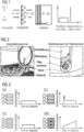
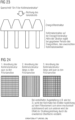
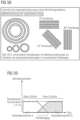
- Figure 1 shows a method for generating a depth profile known from [7]. This involves implanting an ion beam into a substrate through a structured energy filter in an ion implantation system for the purpose of wafer processing. The implantation process and the resulting dopant distribution or defect distribution in the wafer after processing are shown. In particular, it shows how a monoenergetic ion beam is modified in its energy upon passing through a microstructured energy filter component, depending on the entry point. The resulting energy distribution of the ions leads to a modification of the depth profile of the implanted substance in the substrate matrix. This depth profile, which is rectangular in the example shown, is Figure 1 also shown.
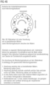
- FIG 2 shows a system for ion implantation.
- This system includes an implantation chamber in which several wafers can be arranged on a wafer wheel.
- the wafer wheel rotates during implantation, so that the individual Wafers repeatedly pass through a beam opening in which the energy filter is located and through which the ion beam enters the implantation chamber and thus into the wafers.
- the wafer wheel is shown, on which the substrates to be implanted are fixed.
- the wheel is tilted 90° and set in rotation.
- the wheel is thus "written” with ions in concentric circles by the ion beam indicated in green.
- To irradiate the entire wafer surface the wheel is moved vertically during processing.
- An energy filter mounted in the beam aperture is shown.
- Figure 3 shows exemplary layouts or three-dimensional structures of filters to illustrate in principle how a variety of different dopant depth profiles can be generated by a suitable choice of filter.
- the individual, in Figure 3 The filter profiles shown can be combined to obtain additional filter profiles and thus doping depth profiles. Shown are cross-sections of the energy filter (leftmost in each figure), top views of the energy filters, and curves of the achieved doping concentration across the wafer depth (as a function of depth).
- the "depth" of the wafer is a direction perpendicular to the wafer surface into which the implantation takes place.
- (a) triangular prism-shaped structures result in a rectangular doping profile
- (b) smaller triangular prism-shaped structures result in a less deep rectangular doping profile compared to case (a) (the depth of the profile can therefore be adjusted via the size of the structures)
- (c) trapezoidal prism-shaped structures result in a rectangular doping profile with a peak at the beginning of the profile
- (d) pyramid-shaped structures result in a triangular doping profile that increases into the depth of the substrate.
- Doping depth profiles in semiconductor wafers can be created by in-situ doping during epitaxial deposition or by (masked) monoenergetic ion implantation.
- High inaccuracies can occur with in-situ doping.
- Even with homogeneous doping profiles significant deviations from the target doping can be expected on the wafer due to the process, i.e., from center to edge.
- this inaccuracy also extends to the vertical direction of the doping region, since the local dopant concentration depends on a multitude of process parameters such as temperature, local doping gas concentration, topology, width of the Prandtl junction, growth rate, etc.
- the use of monoenergetic ion beams means that many individual implantations must be performed to obtain doping profiles with acceptable vertical ripples. This approach is only partially scalable and quickly becomes economically unviable.
- the energy filter is a highly fragile microstructured membrane, making non-destructive handling difficult.
- non-experts i.e., non-engineers
- it must be ensured that, after a brief introduction, even non-experts (i.e., non-engineers) should be able to replace the filter after wear or during a tool change on the implanter system.
- New semiconductor devices such as superjunction devices or optimized diode structures require a non-uniform doping profile.
- the simple energy filters described in [1-6] only produce constant profiles.
- More complicated Filter structures such as those described in Hinb [8] are technically very complex and difficult to implement for productive purposes based on the current state of the art. The challenge is to realize complex vertical profile shapes with uncomplicated, ie, easily manufactured, filter structures.
- Production conditions mean, for example, that more than typically 20-30 wafers with a 6" diameter and area doses per wafer of approximately 2E13cm-2 are to be produced per hour on ion implanters (typical terminal voltage on tandem accelerators > 1MV to 6MV).
- ion implanters typically terminal voltage on tandem accelerators > 1MV to 6MV.
- ion currents of more than 1p ⁇ A up to several 10p ⁇ A must be used or power of more than several watts, e.g. 6W/cm-2, must be deposited on the filter (typical area 1-2cm 2 ). This leads to the filter heating up.
- the task then arises of cooling the filter using suitable measures.
- Filter structures can be manufactured using anisotropic wet-chemical etching.
- the filter structures consist of suitably dimensioned, long, triangular lamellae (e.g., 6 ⁇ m high, 8.4 ⁇ m spacing, a few millimeters long) arranged periodically on a membrane that is as thin as possible.
- triangular lamellae e.g., 6 ⁇ m high, 8.4 ⁇ m spacing, a few millimeters long
- the production of pointed, triangular lamellae is cost-intensive because the wet-chemical anisotropic etching must be precisely adjusted.
- Pointed, i.e., non-trapezoidal lamellae are complex to manufacture because, for pointed lamellae, etching rates and etching times must be precisely coordinated.
- the energy filters for ion implantation described in the cited publications [2], [3], [4], [5], [6], [7], [8], [9], [10] have an internal 3-dimensional structure that leads to path length differences of the ions when transmitted through the filter. These path length differences produce, depending on the stopping power of the filter material, a modification of the kinetic energy of the transmitted ions. A monoenergetic ion beam is thus converted into a beam of ions with different kinetic energies. Energy distribution is determined by the geometry and materials of the filter, i.e., the filter structure is transferred into the substrate by ion lithography.
- the angular spectrum of the transmitted ions must be restricted to avoid "under-implantation" of the masking layer.
- Electrons from the primary beam can be released or absorbed by the solid, i.e., depending on the properties of the filter material and the primary energy, the transmitted ions have, on average, a higher or lower charge state after passing through the filter [26]. This can lead to positive or negative charging of the filter.
- the energy filter will heat up, see Fig. 6.5.24. Due to thermionic electron emission (Richardson-Dushman law), thermal electrons are generated depending on the temperature and the work function of the filter material.
- Publications [2] - [15] propose microtechnical processes for the production of energy filters.
- they describe the use of lithography processes in combination with wet-chemical or dry-chemical etching processes.
- the preferred method for filter production is the anisotropic wet-chemical etching process using alkaline etching media (e.g., KOH or TMAH) in silicon.
- the functional filter layer is made of monocrystalline silicon. Therefore, when bombarded with high-energy ions, it must always be assumed that channeling effects will influence the effective energy loss in the filter layer in a way that is difficult to control.
- An irradiation arrangement must be used that allows a static or moving substrate to be energy-filtered with high lateral homogeneity over the entire Irradiating the substrate surface while utilizing a large filter area. This can reduce thermal effects and degradation effects in the filter.
- the energy filter is a tool for manipulating the doping profile in the substrate.
- manipulation of the achievable doping profile in the substrate AFTER the energy filter is desirable.
- "pushing" the near-surface start of the doping profile out of the substrate is desirable. This can be particularly advantageous if the start of the doping profile in the substrate cannot be correctly adjusted by the filter for various reasons (particularly loss of ions due to scattering).
- Such doping profile manipulation after the energy filter can be achieved by implantation into a sacrificial layer on the substrate.
- the position of, for example, a horizontal irradiated line on the wafer is coupled to a specific vertical position on the multifilter.
- a gap between individual filter elements, for example, would result in an inhomogeneously doped line on the wafer. Therefore, the filter components in the multifilter must be arranged in such a way that lateral homogeneity is ensured despite the coupling of the linear movements of the filter and substrate.
- the filter held therein can have any surface structure selected according to the desired doping profile to be achieved.
- the filter holder and/or the filter frame can be provided with a coating that prevents material removal from the filter frame and filter holder.
- Filter frames and filter holders can be made of metals, preferably stainless steel or similar.
- sputtering effects in the local area of the energy filter must be expected due to scattered ions, i.e., near-surface removal of frame and filter holder material must be expected.
- Metal contamination on the substrate wafer could be an undesirable consequence.
- the coating prevents such contamination, whereby the coating consists of a non-contaminating material. Which substances are non-contaminating depends on depends on the properties of the target substrate used. Examples of suitable materials include silicon or silicon carbide.
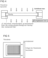
- Figure 4 shows a cross-section of a filter frame for accommodating an energy filter chip.
- the energy filter chip which is Figure 4 also shown, can be fixed in the frame in various ways, such as by gluing using a vacuum-tight, temperature-stable and highly heat-conductive adhesive or by a mechanical spring.
- Figure 5 shows a top view of a filter frame for receiving an energy filter element, which is Figure 5 is also shown.
- the filter frame has a locking element through which the frame can be opened and closed to change the energy filter.
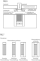
- Figure 6 illustrates an example of the installation of a frame for accommodating an energy filter element in the beam path of an ion implanter. Shown in the upper part of Figure 6 A cross-section through the chamber wall and the filter holder arranged thereon.
- the filter holder is arranged on the inside of the chamber wall, i.e. the side facing the wafer (not shown) during implantation.
- the ion beam passing through the opening in the chamber wall and the filter arranged in front of the opening during implantation is in Figure 6 also shown schematically.
- the frame with the filter chip inserted into the filter holder covers the opening in the chamber wall through which the ion beam passes during implantation. This is shown in the lower part of the Figure 6 which shows a top view of the chamber wall with the filter holder attached to it.
- the frame may be made of the same material as the filter.
- the frame may be manufactured monolithically with the filter and referred to as a monolithic frame.
- the frame may also be made of a different material than the filter, such as a metal.
- the filter may be inserted into the frame.
- the frame comprises a monolithic frame and at least one further frame made of a different material than the filter, which is attached to the monolithic frame.
- This further frame is, for example, a metal frame.
- the frame can completely surround the filter, as explained and shown above and as shown on the right in Figure 7 is shown.
- the frame does not border all (four) sides (edges) of the filter, but only borders three, two (opposite) or only one of the edges of the filter.
- a frame is therefore to be understood as a full frame that completely surrounds the filter on the sides (edges), but also as a partial frame that only partially surrounds the filter on the sides. Examples of such partial frames are shown in Figure 7 also shown.
- Figure 7 shows different A partial frame (left in the figure) and a full frame (far right in the figure).
- These frames can be made of the same (e.g., monolithic) and/or a different material than the energy filter.
- the energy filter or any other scattering element can be mounted in the beam path of the implanter in various ways through its frame, which can be implemented according to one of the examples explained above. Inserting the frame into a filter holder, as explained above, is just one of several possibilities. Further possibilities are explained below.
- the frame can be attached to the chamber wall by at least one web.
- the at least one web serves as a filter holder.
- Figure 8 Examples of fastenings with only one bar, two bars, and three bars. Of course, more than three bars can also be provided.
- the frame can also be attached to the chamber wall using suspensions or suspension elements.
- suspensions or suspension elements are, for example, flexible and can be stretched between the frame and the chamber wall in such a way that the frame is held firmly.
- the suspension elements act as filter holders. Shown in Figure 9 Examples of mountings with a single suspension, two suspensions, and three suspensions. Of course, more than three suspensions can also be provided.
- the frame with the filter is held in a suspended (contactless) manner by magnets.
- magnets are attached to a front and a back of the frame and to the chamber wall in such a way that a magnet on the chamber wall or a holder attached to the chamber wall is opposite a magnet on the frame, with opposite poles of the opposing magnets facing each other.
- the magnetic forces hold the frame in a suspended manner between the magnets attached to the chamber wall or the holder.
- the magnets on the frame of the filter can be realized, for example, by thermal vapor deposition or any other layer-applying process.
- the geometric design of an energy filter for ion implantation systems allows the realization of any desired doping profile in a semiconductor material.
- the decomposition of a doping depth profile is not limited to the triangular structures shown here; it can also include other structures, which in the most general case contain slopes or convex or concave rising flanks.
- the flanks do not necessarily have to be monotonically rising, but can also contain valleys and dips. Binary structures with flank angles of 90° are also conceivable.
- the filter elements are cut "slanted" and arranged directly next to each other.
- the angled cut has the advantage that no adhesive bond is required between the filters to block ions at the filter edge. Furthermore, this allows for optimal use of the irradiated area. With the same overall filter dimensions and a given ion current, this increases wafer throughput.
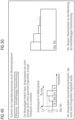
- Figure 11 illustrates an example of a simple implementation of a multi-filter.
- three differently shaped filter elements are combined in a frame of the filter holder to form a complete energy filter.
- Top left is Figure 11 a cross section through the filter holder with the three filter elements is shown and in the bottom left corner Figure 11 a top view of the filter holder with the three filter elements.
- Figure 11 A filter profile that can be achieved with the combined filter is shown. When this filter is used as an implantation filter, the ion beam sweeps over all individual filter elements evenly, so that the right in Figure 11 The dopant depth profile shown is achieved.
- This profile contains three subprofiles numbered 1, 2, and 3. Each of these subprofiles results from one of the three subfilters shown on the left, specifically from the subfilter with the corresponding number.
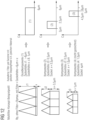
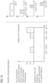
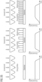
- Figure 12 illustrates the functionality of three different filter elements that can be combined to form a multi-filter. Each figure shows a cross section through the individual filter elements, exemplary dimensions of these filter elements, and dopant profiles that can be achieved by the individual filter elements. For a fourth, not shown, filter element, Figure 12 Only exemplary dimensions are given. The weighting, ie, the resulting concentration or doping profile, can be adjusted by dimensioning the areas of the individual filter elements. For this example, it was assumed that the filter and substrate have the same energy-dependent stopping power, although this may not be the case.
- Figure 13 shows an example of a doping profile that can be obtained when the four Figure 12 explained filter elements are combined to form a multifilter and used for implantation.
- This cumulative profile is obtained by adding the filter elements weighted over the respective area.
- the Figure 12 The filter elements described were assembled with suitable weighting to form a complete filter and were evenly swept over by an ion beam of suitable primary energy, resulting in the cumulative profile shown.
- the individual filter elements of the multifilter are separated from each other by webs of the frame.
- the individual filter elements can also be directly adjacent to one another.
- Figure 14 shows a cross-section through a multi-filter comprising several adjacent filter elements F1, F2, F3, which is inserted into a filter frame.
- the individual filter elements F1, F2, F3 are sawn diagonally and arranged directly adjacent to one another.
- High wafer throughput at given target doping levels can only be achieved with high ion currents. Since between approximately 20% and approximately 99% of the ion beam's primary energy is deposited in the filter membrane, i.e., the irradiated part of the implantation filter, the use of a cooling process is proposed to prevent an excessive increase in the filter temperature, even at high ion currents.
- Such cooling can be achieved, for example, by one or more of the measures explained below under a. to c.:
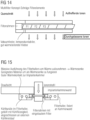
- FIG 15 shows an example of such a cooled filter holder. Shown in particular is a cross-section of a filter holder attached to a chamber wall of an implanter.
- cooling lines are integrated into the filter holder, which accommodates the filter frame. These cooling lines are supplied with coolant by an external cooling device (not shown). Alternatively or additionally, the cooling lines can also be arranged on the surface of the filter holder (not shown).
- the filter or filter holder When using a rotating wafer wheel, for example, loaded with 10-15 wafers, it is proposed to design the filter or filter holder so that it rotates or oscillates with a linear motion.
- the ion beam can be moved electrostatically over the filter with a stationary filter.
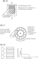
- the filter is only partially irradiated by the ion beam per unit of time. This allows the currently unirradiated part of the filter to be cooled by radiation. This allows for higher average current densities to be achieved for a given filter during continuous operation. Examples of how this can be achieved are described in the Figures 16 and 17 shown.
- Figure 17 illustrates an energy filter with a relatively large area which is only partially irradiated per unit of time. This allows the non-irradiated areas to cool down via radiation cooling.
- This embodiment can also be designed as a multi-filter, as described above. That is, as a filter having several different filter elements.
- the frame with the filter oscillates in a direction perpendicular to the beam direction of the ion beam, which is shown schematically.
- the area of the filter covered by the ion beam is smaller than the total area of the filter, so that only a part of the filter is irradiated per unit of time. This part changes continuously due to the oscillation.
- Figure 18 shows an example of a filter arrangement with multiple filter elements held by a rotating filter holder.
- the individual filter elements can each have the same structure, but can also be structured differently to create a multi-filter.
- the individual filter elements move at Rotation of the holder on a circular path around the rotation axis (central axis) of the holder. In this example, too, only partial irradiation occurs per unit of time, meaning that not all filter elements are irradiated simultaneously, allowing the non-irradiated filter elements to cool down.
- microstructured membrane e.g., spike structure
- a plateau on the spikes instead of a tip
- dimension the thickness of the membrane support layer in such a way that the resulting low-energy dopant peak is pushed into the support layer of the filter and thus is not implanted into the substrate.
- An example of such a filter is described in Figure 18 Shown are a cross-section (left in the figure), a top view (center), and an example of a doping profile that can be achieved by the filter shown.
- a rectangular profile can be created in the substrate by implanting ions into the energy filter using a trapezoidal prism-shaped structure.
- the initial peak is implanted into the energy filter, meaning no peak of the doping profile is present within the substrate.
- the implantation profile has the advantageous property that it begins directly at the substrate surface, which can be crucial for the application of the energy filter.
- this filter structure has plateaus instead of spikes, meaning the individual structural elements are trapezoidal in cross-section.
- lateral homogeneity can be crucial in static implantation situations.
- a rotating wafer disk wafer wheel
- homogeneity is determined by the rotational and translational motion of the wafer disk relative to the ion beam.
- Filter-substrate distance The angular distribution of the transmitted ions is energy-dependent. If the filter and the ion energy are matched so that, among other things, very low-energy ions (nuclear deceleration regime) leave the filter, the angular distribution is broad, since large-angle scattering events occur frequently. If the filter and the ion energy are matched so that only high-energy ions (only in the electronic regime, dE/dx electron > dE/dx nuclear ) leave the filter, the angular distribution is very narrow.
- a minimum distance is characterized by the fact that the structure of the filter is not transferred into the substrate, i.e., for example, that for a given scattering angle distribution of the transmitted ions, these cover at least a lateral distance comparable to the period of the lattice constant of the ion filter.
- a maximum distance is determined by the loss due to scattered ions that can still be tolerated by the application (semiconductor component) for a given scattering angle distribution, especially at the edge of the semiconductor wafer.
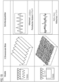
- Figure 19 This is the result of an experiment in which ions were implanted through an energy filter during a static implantation into a PMMA (polymethylacrylate) substrate.
- the ions disrupt the molecular structure of the PMMA, allowing a subsequent development process to reveal the energy distribution of the ions in such a way that areas of high energy deposition are dissolved. Areas with low energy deposition or no energy deposition by ions are not dissolved in the developer solution.
- the idea proposed here is to generate a high lateral doping homogeneity for both dynamic and static implantation arrangements by correctly choosing the filter-substrate distance.
- the filter's chemical composition, density, and geometry are modified in such a way that the effects on the target profile to be achieved can no longer be neglected.
- a database stores, for example, the signatures of the filters that can be used on a specific implanter and their properties, such as which process (ion type, energy) the filter is suitable for, which accumulated dose, and which maximum temperature may be reached.
- the control computer can thus determine whether the filter is suitable for a planned implantation process.
- Figure 20 illustrates a control system for identifying the filter and monitoring compliance with the filter specification (maximum temperature, maximum accumulated ion dose).
- the built-in sensors charge integrator and temperature sensor
- the implantation process is terminated if one of the specified parameters is reached or exceeded, for example, if the filter becomes too hot or the permitted maximum dose has been implanted through the filter. This means that if the specification is violated, a signal is sent to the control computer, which terminates the implantation process.
- a masking layer can be applied to the target substrate.
- collimate the ion beam transmitted through the filter collimate the ion beam transmitted through the filter. Collimation can be achieved using stripe, tube, grid, or hexagonal structures with high aspect ratios, which are placed after the energy filter in the transmitted beam. The aspect ratio of these structures defines the maximum allowable angle.
- Figure 21 shows a cross-section of an implanter chamber wall in the area of the beam opening, a filter holder attached to the chamber wall with an inserted filter, and a collimator, which in the example is attached to a side of the filter holder facing away from the chamber wall.
- An aspect ratio of the collimator which is determined by the length and width of the collimator, determines the maximum angle ⁇ relative to the longitudinal direction of the collimator at which the ion beam can be radiated into the collimator in order to pass through the collimator. Portions of the ion beam that are radiated at larger angles end at the wall of the collimator and therefore do not pass through it.
- the collimator can also consist of several collimator units with smaller openings arranged next to one another. These can, for example, be arranged in a honeycomb pattern.
- the collimator structure can be arranged directly on the filter element.
- Such an element can be manufactured monolithically or by microbonding.
- Two examples of such a collimator structure arranged directly on the filter are shown in Figure 22 shown.
- Such a collimator structure arranged directly on the filter can mechanically stabilize the filter and also have a cooling effect, since the collimator structure can act as a heat sink with a larger surface area compared to the filter.
- the maximum angle ⁇ is also defined here by the aspect ratio of the individual collimator structures arranged on the filter, each of which has a length and a width.
- the collimator structure can be attached to the filter, for example, by gluing, bonding, or similar means.
- the collimator structure is located on the structured side of the filter, i.e., where the filter has elevations and depressions.
- the structures are trapezoidal.
- Figure 23 shows a modification of the arrangement of Figure 22
- the collimator structure is located on the unstructured side of the filter.
- the collimator structure is in Beam direction of the ion beam (which is shown in the Figures 21 and 22 symbolized by the arrow) is arranged after the filter, so that the ion beam passes the collimator structure after passing the filter.
- Figure 24 shows top views of collimator structures according to various examples.
- this collimator structure is arranged on a filter that has a lamellar structure in plan view.
- the individual "filter leaves” can be triangular or trapezoidal in cross-section, for example, as previously explained.
- a lamellar structure of the filter is only an example. Any other filter structures, as previously explained, can also be used.
- the left part and the middle shows Figure 24 One example each in which the collimator structure is strip-shaped, i.e., has several parallel strips, each extending across the entire width of the filter. Two adjacent strips form a collimator, with the width of this collimator being determined by the spacing between the adjacent strips.
- the length of the collimator is determined by the height of the individual strips.
- the "height" of the strips is their dimension in a direction perpendicular to the plane of the drawing.
- the strips of the collimator structure can run perpendicular to the filter blades, as shown on the left in Figure 24 shown, or can run parallel to the slats, as shown in the middle.
- the collimator structure has a grid-like shape in plan view, forming a plurality of collimators whose geometry is determined by the geometry of the grid.
- the individual collimators are rectangular in plan view, in particular square, so that the collimators are rectangular tubes.
- the grid can also be implemented such that the individual collimators are circular, elliptical, or hexagonal (honeycomb-shaped) in plan view, or have any other polygonal geometry.
- a mask acting as a collimator structure can be applied to the target wafer as an alternative or in addition to a collimator on the filter.
- One requirement for this masking may be that the stopping power of the mask must be at least equal to the average range of the transmitted ion beam in the target substrate material.
- the aspect ratio of the mask can be adjusted accordingly.
- Figure 25 shows an example of such a collimator structure arranged directly on the target substrate.
- This collimator structure can have any of the previously explained geometries, for example lamellar, strip-shaped, tubular or honeycomb-shaped - depending on the layout of the substrate structure and the required maximum angular distribution.
- the aspect ratio of this collimator structure is the ratio of height (h in Figure 25 ) to width (b in Figure 25 ) of the recesses of the mask forming the collimator structure on the substrate.
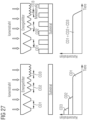
- FIG. 26 This figure shows the doping profiles for three different implantation processes, each performed with the same filter but different collimator structures.
- the filter has a lamellar structure with a trapezoidal cross-section.
- the left part of the figure illustrates an implantation process in which implantation is performed without a collimator structure. The resulting implantation profile begins at the surface of the substrate.
- FIG. 26 Implantation processes are illustrated in which a collimator structure is used for implantation, whereby the aspect ratio of the collimator structure is higher in the example shown on the right than in the example shown in the middle.
- the doping profiles obtained by these implantation processes do not begin at the surface of the substrate but at a distance from it, with the doping profiles being further away from the surface and the more gently they rise the higher the aspect ratio. This can be explained by the fact that the dopant profile in the region near the surface of the substrate is caused by ions that are slowed down more strongly in the filter and therefore have a lower energy.
- Such low-energy ions are scattered more strongly by the filter than ions with higher energy, so that these low-energy ions have a larger angular distribution than ions with higher energy.
- more ions with low energy than ions with higher energy no longer pass through the collimator structure, whereby this effect is more pronounced the larger the aspect ratio of the collimator structure, i.e. the smaller the maximum angle at which the ions can still pass through the collimator structure.
- the filter can be designed to "prefer" low-energy ions, meaning that more low-energy ions than higher-energy ions pass through the filter.
- An example of such a filter is shown in Figure 27 shown.
- the filter has different filter areas, each with a maximum and a minimum thickness. The maximum thickness is the same in all three areas, but the minimum thickness is different. This is achieved in the example by having the filter in each area have a base area arranged trapezoidal structure, whereby the height of the base has different thicknesses or the trapezoidal structures have different heights.
- the thickness of the base is at its thinnest and the trapezoidal structure is at its highest, whereby a distance CD1 between adjacent structures in this section is the greatest.
- the thickness of the base is at its greatest and the trapezoidal structure is at its lowest, whereby a distance CD3 between adjacent structures in this section is the smallest.
- the thickness of the base lies between the thickness in the first section and the thickness in the third section, accordingly a height of the trapezoidal structure in this section is between the height in the first section and in the third section and a distance CD2 between adjacent structures in this section is between the distance CD1 in the first section and the distance CD3 in the third section.
- the individual sections can each be the same size in terms of their area, but can also be different sizes. Furthermore, more than three sections with different minimum filter thicknesses can of course be provided.
- Figure 27 The left-hand part shows an implantation profile obtained when implanting with the described filter, when implanting without a collimator structure. This implantation profile begins at the surface, but the doping concentration decreases gradually with increasing depth.
- CD1 denotes a region of the doping profile caused by the first section of the filter
- CD2 denotes a region of the doping profile caused by the second section of the filter
- CD3 denotes a region of the doping profile caused by the third section of the filter.
- the doping profile shows that the ions passing through the respective filter region penetrate less deeply into the substrate, i.e., the greater the minimum thickness of the base of the respective section, the lower their energy.
- the doping profile shows that more low-energy ions than high-energy ions pass through this filter.
- the ions with low energy are scattered more strongly than the ions with higher energy, and thus fewer ions with low energy than ions with higher energy pass through a collimator structure
- using such a filter in conjunction with a collimator structure can achieve an almost homogeneous doping profile starting at the surface.
- This is shown on the right in Figure 27 , which illustrates an implantation process using the described filter and a collimator structure.
- the collimator structure is located on the substrate in the example, but can also be arranged on the filter.
- Implantation arrangement of the filter towards the substrate, one spike towards the substrate, one spike away from the substrate ⁇ sputtering, scattering upon impact.
- the filter can be used in such a way that the microstructures of the filter face the substrate, i.e., point away from the ion beam, as in Figure 28 (a)
- the filter can be rotated so that the microstructures of the filter are facing away from the substrate, i.e. towards the ion beam, as shown in Figure 28 (b)
- the latter can have beneficial effects on sputtering effects in the filter.
- Channeling should therefore be avoided. Tilting the filter and substrate can prevent channeling. Channeling in the filter or in the substrate can have very different effects on the depth profile of the implanted dopant, especially if the filter and substrate are made of different materials.
- Figure 29 This schematically shows a filter that is tilted relative to the substrate during the implantation process such that a base area of the filter forms an angle with a surface of the substrate that is greater than zero.
- This angle is, for example, greater than 3°, greater than 5°, or greater than 10° and less than 30°. This can prevent or reduce a channeling effect, especially when the energy filter is made of anisotropic materials.
- Figure 30 shows a schematic representation of different doping profiles (doping concentration as a function of depth in the substrate) for differently shaped energy filters, each shown in side and top views.
- triangular prism-shaped structures produce a rectangular doping profile
- smaller triangular prism-shaped structures produce a less depth-distributed doping profile than the larger triangular prism-shaped structures shown in (a)
- trapezoidal prism-shaped structures produce a rectangular doping profile with a peak at the profile beginning
- pyramid-shaped structures produce a triangular doping profile that increases with the depth of the substrate.
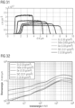
- Figure 32 illustrates the course of the deceleration capacity as a function of energy [4] (SRIM simulation) for the different substrate materials, which correspond to the representation in Figure 31 underlie.
- Figure 33 illustrates a multilayer starting material for a multilayer filter.
- this starting material comprises four different layers, designated 1 to 4.
- the use of four layers is only an example. Fewer or more than four different layers can also be used.
- the individual layers can differ not only in terms of the material used but also in their thickness. It is also possible for two layers to be made of the same material and separated by two or more layers of different materials. The individual layers can be deposited or produced sequentially on top of one another using suitable deposition processes.
- Figure 34 shows a cross-section of a filter based on the Figure 33 manufactured starting material and which, in the example shown, has a base and triangular structures arranged on the base. These triangular structures can be strip-shaped, i.e. elongated in a direction perpendicular to the plane of the drawing, or can be part of pyramid-shaped structures.
- the filter can also be implemented such that several structures are arranged side by side in the lateral direction (y-direction), which have different geometries and/or different layer stacks, i.e., layer stacks with different structures with respect to the sequence of individual layers and/or the material of the individual layers.
- the filter shown uses six different materials, designated 1-6.
- Suitable materials for the individual layers include, but are not limited to, silicon, silicon compounds, or metals.
- silicon compounds include silicon carbide (SiC), silicon oxide ( SiO2 ), or silicon nitride (SiN).
- Suitable metals include copper, gold, platinum, nickel, or aluminum.
- at least one layer of a silicon compound is grown on a silicon layer, and a metal layer is vapor-deposited onto the at least one layer of a silicon compound.
- a metal layer can also be vapor-deposited directly onto a silicon layer. It is also possible to produce different metal layers on top of one another by vapor deposition, in order to create different layers of the filter.
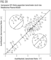
- Figure 36 illustrates the equilibrium charge states of an ion (black line: Thomas-Fermi estimate, blue line: Monte Carlo simulations, red line: experimental results) as a function of the ion's kinetic energy when irradiating a thin membrane.
- Ion sulfur
- membrane carbon.
- the distance (in high vacuum) between the filter and the substrate of the ion accelerator is typically only a few centimeters or less. This means that the diffusion of thermal electrons (from thermionic emission) and the effect of fast electrons (from ion bombardment) distort the measurement of the ion current at the substrate, for example, by a Faraday cup attached there.
- the figure shows a cross-section of a filter arrangement that ensures this.
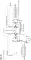
- the filter in the filter frame is held at a defined (positive) potential relative to the filter holder to suppress secondary electrons.
- the filter frame is connected to a voltage source and electrically insulated from the filter holder and the chamber wall of the implanter.
- the electrical potential of the filter holder can be regulated. For example, such that, regardless of the charge balance resulting from the implantation process, a constant potential is established during implantation compared to the potential of the substrates to be implanted or to ground potential. For this purpose, a controlled supply of positive or negative charge can be provided by a current source.
- the potential to be set can be selected in such a way that, for example, the emission of electrons from the filter is completely suppressed, thus only measuring the (positive) charge of the transmitted ion current in the Faraday cup next to or on the substrate.
- Typical values for such a (positive) potential are between a few tens of V and a few thousand V.
- the energy filter is very high-impedance due to its material properties
- the stopping power of this layer must be included in the overall stopping power balance when designing the filter. Care must be taken to ensure that the applied layer (even when applied to the side facing away from the substrate) does not, in principle, cause any harmful contamination in the substrate material to be implanted.
- the layer can be made of carbon, for example.
- the stopping power of this layer should be considered in the overall stopping power balance when designing the filter. Care must be taken to ensure that the applied layer (even when applied on the side facing away from the substrate) does not cause any harmful contamination in the substrate material to be implanted.
- Ad 12 Alternative manufacturing methods using injection molding, casting or sintering processes
- a further advantage is that by using the molding processes mentioned, the costs for producing a large number of filter elements can be significantly reduced compared to microtechnical production.
- FIG. 40 shows an arrangement for implantation into a substrate through an energy filter. This arrangement includes a deflection device for the ion beam, which is arranged in front of the filter.
- the deflection of the ion beam which can be achieved by this deflection device, is adapted to the distance between the filter and the substrate (typically in the range of a few cm to a few m) so that the substrate can be completely irradiated, i.e., across its entire surface, for the purpose of implantation.
- Ad 14 Arrangement for utilizing a large filter area
- Figure 41 illustrates an arrangement for an energy filter implantation (i.e., an implantation by means of an energy filter), in which the beam area has been enlarged by suitable measures and the irradiated filter area is larger than the substrate area, whereby a complete irradiation of the substrate can be achieved and a large filter area can be used.
- the irradiated filter area diameter is larger than the substrate diameter.
- filter structures are "large.”
- penetration depths of > 100 ⁇ m are required. Therefore, filter structures with "peen heights” of > 100 ⁇ m are required for this application.
- Such filter structures can be manufactured very easily with sufficient mechanical stability, even for large substrates (e.g., 6" or 8").
- a minimum distance between the substrate and the filter should be maintained to ensure that there is sufficient lateral homogenization of the implanted ions due to scattering effects.
- the filter consists of an arrangement of a number of, for example, strip-shaped filter elements. These filter elements can, for example, be manufactured monolithically from a substrate using suitable manufacturing processes.
- the other (inactive) part of the filter area is used to stabilize the filter membrane. This part shades the ion beam. Therefore, in this arrangement, either the substrate or the filter must be moved to compensate for the shadowing effects.
- Figure 42 illustrates a partially active filter with mechanical scanning in one direction.
- Ad 15 Modification of the doping profile in the substrate using a sacrificial layer
- a sacrificial layer can be applied to the substrate, the thickness and stopping power of which are suitably selected so that the implantation profile is shifted in its depth within the substrate as desired.
- a sacrificial layer can be used for masked ion implantation (see Figure 43 ) or for unmasked ion implantation.
- this method can be used to "push out" an unwanted beginning of a doping profile from the substrate into the sacrificial layer by implanting the beginning of the profile into the sacrificial layer.
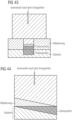
- Figure 43 illustrates a modification of the doping profile in the substrate using a sacrificial layer in the case of a masked, energy-filtered implantation.
- the beginning of the implantation profile is shifted into the sacrificial layer.
- This principle can be used analogously for an unmasked, energy-filtered ion implantation, i.e. an implantation in which, unlike in Figure 43 shown no mask layer is present.
- a sacrificial layer is applied to the substrate, the stopping power and thickness of which are suitably selected across the wafer surface so that the implantation profile is shifted in its depth within the substrate as desired, depending on the lateral position on the wafer.
- Such a sacrificial layer can be used for masked ion implantation or for unmasked ion implantation (see [Fig. Figure 44 ).
- changing the implantation depth of a homogeneous doping profile can be advantageously used for edge terminations in semiconductor devices.
- Figure 44 illustrates a lateral modification of the doping profile in the substrate using a sacrificial layer in the case of an unmasked, energy-filtered ion implantation.
- a lateral modification of the implantation depth is achieved by varying the thickness of the sacrificial layer in the lateral direction.
- the principle can be applied analogously for masked, energy-filtered implantations.
- Ad 17 Adjustment of a profile transition of several implantation profiles
- Two or more doping profiles can be cleverly overlapped to create a desired overall doping profile, particularly in the overlap region. This technique is particularly advantageous when growing and doping multiple layers.
- a representative example is the growth of multiple SiC epi layers and their respective energy-filtered doping. Good contact between the layers should be ensured.
- Ad 18 Special arrangement of the multi-filter concept with coupled pendulum movement
- a clever arrangement can be used so that despite the coupled pendulum motion of filter and substrate, i.e. no relative vertical movement between filter and substrate, a lateral homogeneity of the ion distribution is achieved.
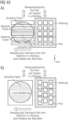
- Such an arrangement is Figure 45 shown.
- the wafers are guided along behind the substrate by the rotation of the wafer wheel in the x-direction.
- the ion beam (not shown), for example, is expanded in the x-direction and is scanned across the entire multi-filter area by the vertical pendulum motion of the implantation chamber.
- the area consists of active filter areas and inactive support areas.
- Arrangement A) is an unfavorable arrangement.
- Arrangement A is a rather unfavorable arrangement. If one considers the irradiated filter area for y1 and y2, three filters are irradiated at y1, while no filter is irradiated at y2. The result is a laterally inhomogeneous stripe pattern on the wafer.
- Arrangement B shows a possible example of a better arrangement. Two filters are irradiated for both y1 and y2. This applies to all y. This achieves laterally homogeneous doping across the wafer area.
- Another aspect is intended to solve the problem of monitoring important parameters of the ion implantation modified by an energy filter.
- Such parameters include, for example, the minimum or maximum projected range, the depth concentration distribution adjusted by the filter geometry, and the (energy-dependent) angular distribution.
- Monitoring additional parameters such as the implanted ion species, etc., could also be useful.
- Monitoring should be possible, in particular, on the wafers to be implanted or on (several parallel) structures arranged near the wafers. According to one aspect, monitoring should be carried out without further processing of the monitoring structures or the wafers.
- Monitoring can be performed by measuring optical parameters such as spectral absorption, spectral transmission, spectral reflection, changes in the refractive index, global absorption (wavelength range depends on the measuring device) and global transmission, as well as reflection (wavelength range depends on the measuring device).
- optical parameters such as spectral absorption, spectral transmission, spectral reflection, changes in the refractive index, global absorption (wavelength range depends on the measuring device) and global transmission, as well as reflection (wavelength range depends on the measuring device).
- masks and substrate materials for monitoring the implantation parameters mentioned which (1) are arranged at a suitable location on the surface to be implanted, e.g. wafer wheel, and (2) by ion implantation, their e.g. optical properties "as implanted", ie without further post-processing such that, for example, the change is proportional to the implanted ion dose for a given ion type.
- Materials mentioned under (2) include PMMA (Plexiglas), PMMA, SiC, LiNbO3, KTiOPO4, and similar.
- the target substrate e.g. a SiC wafer
- the target substrate can be used directly for optical monitoring.
- the depth (or the etch rate, or the resulting etch geometry, etc.) of a structure modified after ion irradiation can be considered a measure of the implanted ion dose.
- Such changes could include, for example, mechanical properties of the monitor material, electrical properties of the monitor material, or even the nuclear activation of the monitor material due to high-energy ion irradiation.
- detection is to be achieved via changes in optical properties.
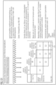
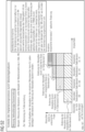
- a monitoring structure consists of the arrangement of a suitable substrate material with one or more mask structures. Examples are described in the Figures 47 and 48 shown.
- the monitoring structure or structures are as in Figure 46 As shown, they are arranged at a suitable location, for example, on the wafer wheel.
- the monitoring chips are read out after implantation, for example, without further post-processing. If necessary, the mask must be separated from the monitoring substrate for the readout measurement. According to one aspect, the mask is reusable.
- the mask material and substrate material of the monitoring chip can be made of different materials.
- the criteria for selecting the mask material include compatibility with the material of the target substrate (to exclude contamination from sputtering effects) and a deceleration capacity for high-energy ions such that mask structures with high aspect ratios can be produced.
- the mask material and substrate material of the monitoring chip can be made of the same material.
- the mask and substrate can also be manufactured monolithically. In this case, reuse of either the mask or the substrate is usually not possible.
- the Figure 50 The mask structures shown or described are staggered in thickness and number depending on the desired depth resolution, or are designed as an "inclined plane" or a continuous ramp. For the largest thickness, for example, the following applies: "Mask thickness"> Rp, max.
- the lateral dimensions of the individual structures can range from square micrometers to square millimeters to square centimeters, depending on the requirements of the readout equipment.
- Analog structures can also be used to measure or monitor the minimum projected range using evaluation procedures as described under A.
- the energy filter for ion implantation produces an energy-dependent spectrum of ion angles after passing through the filter.
- the resulting angular distribution is thus a function of the filter geometry, the change in geometry during the filter's lifetime, the occurrence of channeling effects, the ion species used, the primary energy, the resulting maximum and minimum energies of the transmitted ions, and the geometric arrangement in the implantation chamber. All of these parameters can be monitored by monitoring the angular distribution.
- the opening sizes of the mask structures for thin masks that are only slightly thicker than the maximum projected range in the mask material can be in the micrometer or submicrometer range.
- Such monitoring structures are preferably arranged as arrays consisting of many individual structures in order to be able to carry out a global (i.e. on an area of several mm 2 or cm 2 ) optical evaluation.
- the aperture sizes can be in the millimeter or centimeter range. In these cases, the evaluation of individual structures that are not arranged in an array is also possible without excessive technical effort.
- the core of the aspects discussed above is the application of (essentially) dose-dependent modification of the (preferably) optical parameters of a material for "as-implanted" monitoring of the energy filter implantation process. This allows the resulting implantation result to be monitored as completely as possible in its most important parameters using (for example) optical measurement, without the need for complex post-processing (e.g., annealing and application of metallic contacts).
- Figure 59 illustrates a clever adaptation of a profile transition between two implantation profiles A and B, so that the resulting overall concentration profile can, for example, produce a desired homogeneous profile. This can (but does not necessarily) be advantageous, especially for layer systems consisting of two layers, as shown in the image here.
- the low-energy tail of Implant B can be influenced, in particular, by introducing a sacrificial layer, as described in "15: Modification of the Doping Profile in the Substrate Using a Sacrificial Layer.” Proposal for implementation with the following process sequence: 1) Growth of the sacrificial layer. 2) Doping of the lower layer (Implant B). 3) Removal of the sacrificial layer. 4) Growth of the upper layer. 5) Doping of the upper layer.
- the concepts explained above enable production-ready implantation processes for the semiconductor industry, i.e., the economical application of implantation processes in an industrial production process.
- the concepts explained above particularly enable a very flexible (multi-filter concept) implementation of complex vertical doping concentration profiles with a narrow angular distribution of the implanted ions.
- all types of doping concentration profiles can be approximated by using triangular filter structures in conjunction with collimator structures.
- Another important aspect concerns the suppression of artifacts that distort the ion current measurement on the substrate.
- Ad 1 to Ad 19 can be used individually or in any combination.
- the "end-of-life" detection explained above can be applied to a filter held by a frame, but can also be applied to a filter held in another way.
- the wafer explained above can be a semiconductor wafer, but can also consist of another material to be implanted, such as PMMA.
Landscapes
- Chemical & Material Sciences (AREA)
- Analytical Chemistry (AREA)
- Physics & Mathematics (AREA)
- Spectroscopy & Molecular Physics (AREA)
- Engineering & Computer Science (AREA)
- General Engineering & Computer Science (AREA)
- High Energy & Nuclear Physics (AREA)
- Physical Vapour Deposition (AREA)
- Element Separation (AREA)
- Mechanical Treatment Of Semiconductor (AREA)
Applications Claiming Priority (4)
| Application Number | Priority Date | Filing Date | Title |
|---|---|---|---|
| DE102016106119.0A DE102016106119B4 (de) | 2016-04-04 | 2016-04-04 | Energiefilterelement für Ionenimplantationsanlagen für den Einsatz in der Produktion von Wafern |
| EP17717106.3A EP3440690B1 (fr) | 2016-04-04 | 2017-04-04 | Élément de filtre d'énergie pour installations d'implantation ionique destinées à être utilisées dans la production de tranches |
| PCT/EP2017/058018 WO2017174597A1 (fr) | 2016-04-04 | 2017-04-04 | Élément de filtre d'énergie pour installations d'implantation ionique destinées à être utilisées dans la production de tranches |
| EP21183792.7A EP3926658B1 (fr) | 2016-04-04 | 2017-04-04 | Élément filtrant d'énergie pour installations d'implantation ionique destiné à être utilisé dans la production de plaquettes |
Related Parent Applications (3)
| Application Number | Title | Priority Date | Filing Date |
|---|---|---|---|
| EP17717106.3A Division EP3440690B1 (fr) | 2016-04-04 | 2017-04-04 | Élément de filtre d'énergie pour installations d'implantation ionique destinées à être utilisées dans la production de tranches |
| EP21183792.7A Division EP3926658B1 (fr) | 2016-04-04 | 2017-04-04 | Élément filtrant d'énergie pour installations d'implantation ionique destiné à être utilisé dans la production de plaquettes |
| EP21183792.7A Division-Into EP3926658B1 (fr) | 2016-04-04 | 2017-04-04 | Élément filtrant d'énergie pour installations d'implantation ionique destiné à être utilisé dans la production de plaquettes |
Publications (2)
| Publication Number | Publication Date |
|---|---|
| EP4546375A2 true EP4546375A2 (fr) | 2025-04-30 |
| EP4546375A3 EP4546375A3 (fr) | 2025-08-13 |
Family
ID=58544919
Family Applications (4)
| Application Number | Title | Priority Date | Filing Date |
|---|---|---|---|
| EP17717106.3A Active EP3440690B1 (fr) | 2016-04-04 | 2017-04-04 | Élément de filtre d'énergie pour installations d'implantation ionique destinées à être utilisées dans la production de tranches |
| EP25167441.2A Pending EP4553855A3 (fr) | 2016-04-04 | 2017-04-04 | Elément de filtre d'énergie pour implanteur ionique utilisé dans la production de plaquettes |
| EP25163764.1A Pending EP4546375A3 (fr) | 2016-04-04 | 2017-04-04 | Elément de filtre d'énergie pour implanteur ionique utilisé dans la production de plaquettes |
| EP21183792.7A Active EP3926658B1 (fr) | 2016-04-04 | 2017-04-04 | Élément filtrant d'énergie pour installations d'implantation ionique destiné à être utilisé dans la production de plaquettes |
Family Applications Before (2)
| Application Number | Title | Priority Date | Filing Date |
|---|---|---|---|
| EP17717106.3A Active EP3440690B1 (fr) | 2016-04-04 | 2017-04-04 | Élément de filtre d'énergie pour installations d'implantation ionique destinées à être utilisées dans la production de tranches |
| EP25167441.2A Pending EP4553855A3 (fr) | 2016-04-04 | 2017-04-04 | Elément de filtre d'énergie pour implanteur ionique utilisé dans la production de plaquettes |
Family Applications After (1)
| Application Number | Title | Priority Date | Filing Date |
|---|---|---|---|
| EP21183792.7A Active EP3926658B1 (fr) | 2016-04-04 | 2017-04-04 | Élément filtrant d'énergie pour installations d'implantation ionique destiné à être utilisé dans la production de plaquettes |
Country Status (6)
| Country | Link |
|---|---|
| US (5) | US10847338B2 (fr) |
| EP (4) | EP3440690B1 (fr) |
| JP (6) | JP6831133B2 (fr) |
| CN (2) | CN113035676B (fr) |
| DE (1) | DE102016106119B4 (fr) |
| WO (1) | WO2017174597A1 (fr) |
Families Citing this family (19)
| Publication number | Priority date | Publication date | Assignee | Title |
|---|---|---|---|---|
| DE102016106119B4 (de) | 2016-04-04 | 2019-03-07 | mi2-factory GmbH | Energiefilterelement für Ionenimplantationsanlagen für den Einsatz in der Produktion von Wafern |
| DE102016122791B3 (de) * | 2016-11-25 | 2018-05-30 | mi2-factory GmbH | Ionenimplantationsanlage, Filterkammer und Implantationsverfahren unter Einsatz eines Energiefilterelements |
| WO2018173812A1 (fr) * | 2017-03-22 | 2018-09-27 | 国立研究開発法人日本原子力研究開発機構 | Membrane fonctionnelle pour transmission de faisceaux d'ions, dispositif de ligne de faisceau utilisant une membrane fonctionnelle pour transmission de faisceaux d'ions, dispositif de filtre utilisant une membrane fonctionnelle pour transmission de faisceaux d'ions, et procédé de réglage d'un dispositif de filtre |
| US10217654B1 (en) * | 2018-02-12 | 2019-02-26 | Varian Semiconductor Equipment Associates, Inc. | Embedded features for interlocks using additive manufacturing |
| DE102018114667B3 (de) | 2018-06-19 | 2019-09-19 | Infineon Technologies Ag | Ionenstrahl-moderatorvorrichtung, ionenstrahl-implantationsgerät und ionen-implantationsverfahren |
| DE102019112773B4 (de) * | 2019-05-15 | 2023-11-30 | mi2-factory GmbH | Vorrichtung und Verfahren zur Implantation von Teilchen in ein Substrat |
| DE102019120623B4 (de) | 2019-07-31 | 2024-01-25 | mi2-factory GmbH | Energiefilter zur Verwendung bei der Implantation von Ionen in ein Substrat |
| LU101807B1 (en) * | 2020-05-15 | 2021-11-15 | Mi2 Factory Gmbh | Ion implantation device with energy filter having additional thermal energy dissipation surface area |
| LU101808B1 (en) | 2020-05-15 | 2021-11-15 | Mi2 Factory Gmbh | An ion implantation device comprising energy filter and additional heating element |
| CN111634899B (zh) * | 2020-06-14 | 2022-11-18 | 南开大学 | 一种基于金属-有机框架衍生合成碳包覆磷酸钛钾纳米花的制备方法 |
| US20240038491A1 (en) | 2020-12-17 | 2024-02-01 | mi2-factory GmbH | Ion implantation device with an energy filter and a support element for overlapping at least part of the energy filter |
| EP4238121A1 (fr) * | 2020-12-17 | 2023-09-06 | MI2-Factory GmbH | Ensemble filtre d'énergie pour système d'implantation ionique comportant au moins un élément d'accouplement |
| DE102020134222A1 (de) * | 2020-12-18 | 2022-06-23 | mi2-factory GmbH | Verfahren zur Herstellung eines vorbehandelten Verbundsubstrats und vorbehandeltes Verbundsubstrat |
| EP4281990A1 (fr) | 2021-02-24 | 2023-11-29 | MI2-Factory GmbH | Procédé mis en oeuvre par ordinateur pour la simulation d'une implantation ionique filtrée par énergie (efii) |
| WO2022180037A1 (fr) | 2021-02-24 | 2022-09-01 | mi2-factory GmbH | Procédé mis en œuvre par ordinateur pour simulation d'implantation ionique filtrée par énergie (efii) à l'aide d'un tunnel à ions |
| US11569063B2 (en) | 2021-04-02 | 2023-01-31 | Applied Materials, Inc. | Apparatus, system and method for energy spread ion beam |
| CN114758730B (zh) * | 2022-01-05 | 2024-08-16 | 西安理工大学 | 等离子体活性粒子与绝缘材料表面作用的仿真方法 |
| WO2023140953A1 (fr) * | 2022-01-21 | 2023-07-27 | Axcelis Technologies, Inc. | Graphite à angle d'incidence élevé pour commande de particules avec faisceau d'ions à faible rendement de pulvérisation dédié |
| DE102023103315B4 (de) | 2023-02-10 | 2024-11-28 | Ernst-Abbe-Hochschule Jena, Körperschaft des öffentlichen Rechts | Messvorrichtung, Ionenimplantationsvorrichtung und Verfahren zur ladungsunabhängigen In-Situ-Dosismessung |
Citations (3)
| Publication number | Priority date | Publication date | Assignee | Title |
|---|---|---|---|---|
| DE19652463C2 (de) | 1996-12-17 | 1999-02-25 | Univ Schiller Jena | Verfahren und Vorrichtung zur Herstellung dreidimensionaler Mikrostrukturen beliebiger Form |
| US20020050573A1 (en) | 1998-04-17 | 2002-05-02 | Kabushiki Kaisha Toshiba | Ion implantation apparatus, ion generating apparatus and semiconductor manufacturing method with ion implantation processes |
| US7385209B2 (en) | 2003-04-24 | 2008-06-10 | Haute Ecole Arc Ne-Be-Ju | Micromachining process, system and product |
Family Cites Families (37)
| Publication number | Priority date | Publication date | Assignee | Title |
|---|---|---|---|---|
| US4158141A (en) * | 1978-06-21 | 1979-06-12 | Hughes Aircraft Company | Process for channeling ion beams |
| US4278475A (en) * | 1979-01-04 | 1981-07-14 | Westinghouse Electric Corp. | Forming of contoured irradiated regions in materials such as semiconductor bodies by nuclear radiation |
| GB2078441A (en) * | 1980-06-17 | 1982-01-06 | Westinghouse Electric Corp | Forming impurity regions in semiconductor bodies by high energy ion irradiation |
| GB2089499A (en) * | 1980-12-15 | 1982-06-23 | Ramsey Eng Co | X-ray Radiation Analyser |
| DE3121666A1 (de) * | 1981-05-30 | 1982-12-16 | Ibm Deutschland Gmbh, 7000 Stuttgart | Verfahren und einrichtung zur gegenseitigen ausrichtung von objekten bei roentgenstrahl- und korpuskularstrahl-belichtungsvorgaengen |
| JPH0216726A (ja) * | 1988-05-03 | 1990-01-19 | Varian Assoc Inc | イオン注入量の測定のための方法及び装置 |
| JPH0718584Y2 (ja) | 1988-07-18 | 1995-05-01 | 本州製紙株式会社 | 商品底押出し包装体 |
| JP3187043B2 (ja) * | 1990-11-09 | 2001-07-11 | 株式会社フジクラ | 物理蒸着法による酸化物超電導導体の製造方法 |
| US5604394A (en) | 1992-11-06 | 1997-02-18 | Mitsubishi Denki Kabushiki Kaisha | Image display apparatus |
| JP2616423B2 (ja) * | 1993-12-14 | 1997-06-04 | 日本電気株式会社 | イオン注入装置 |
| JPH08220298A (ja) * | 1995-02-11 | 1996-08-30 | Nissin High Voltage Co Ltd | イオンビーム停止部材 |
| US5972728A (en) * | 1997-12-05 | 1999-10-26 | Advanced Micro Devices, Inc. | Ion implantation feedback monitor using reverse process simulation tool |
| US6294862B1 (en) * | 1998-05-19 | 2001-09-25 | Eaton Corporation | Multi-cusp ion source |
| US6136164A (en) * | 1998-07-15 | 2000-10-24 | United Microelectronics Corp. | Apparatus for detecting position of collimator in sputtering processing chamber |
| JP2000306541A (ja) * | 1999-04-16 | 2000-11-02 | Nippon Steel Corp | イオン注入装置におけるウェーハ温度検出装置 |
| US6639227B1 (en) * | 2000-10-18 | 2003-10-28 | Applied Materials, Inc. | Apparatus and method for charged particle filtering and ion implantation |
| DE10201868C1 (de) * | 2002-01-18 | 2003-07-17 | Siemens Ag | Röntgeneinrichtung |
| JP4072359B2 (ja) * | 2002-02-28 | 2008-04-09 | 株式会社日立製作所 | 荷電粒子ビーム照射装置 |
| DE10239312B4 (de) | 2002-08-27 | 2006-08-17 | Infineon Technologies Ag | Verfahren zur Herstellung eines Halbleiterbauelements mit einer Driftzone und einer Feldstoppzone und Halbleiterbauelement mit einer Driftzone und einer Feldstoppzone |
| US20060043316A1 (en) * | 2003-06-10 | 2006-03-02 | Varian Semiconductor Equipment Associates, Inc. | Ion implanter having enhanced low energy ion beam transport |
| JP2005061663A (ja) * | 2003-08-08 | 2005-03-10 | Takata Corp | イニシエータ、イニシエータ用着火薬、イニシエータの起動方法及びガス発生器 |
| JP2007523440A (ja) * | 2004-02-18 | 2007-08-16 | 学校法人早稲田大学 | イオン注入方法及び装置 |
| DE102005061663B4 (de) * | 2005-12-22 | 2008-07-17 | RUHR-UNIVERSITäT BOCHUM | Ionenimplantationsvorrichtung |
| US7619229B2 (en) * | 2006-10-16 | 2009-11-17 | Varian Semiconductor Equipment Associates, Inc. | Technique for matching performance of ion implantation devices using an in-situ mask |
| US7960708B2 (en) * | 2007-03-13 | 2011-06-14 | University Of Houston | Device and method for manufacturing a particulate filter with regularly spaced micropores |
| US8531814B2 (en) * | 2009-04-16 | 2013-09-10 | Varian Semiconductor Equipment Associates, Inc. | Removal of charge between a substrate and an electrostatic clamp |
| US8461556B2 (en) * | 2010-09-08 | 2013-06-11 | Varian Semiconductor Equipment Associates, Inc. | Using beam blockers to perform a patterned implant of a workpiece |
| JP5909654B2 (ja) * | 2010-09-24 | 2016-04-27 | パナソニックIpマネジメント株式会社 | フィルターデバイス |
| US8440578B2 (en) * | 2011-03-28 | 2013-05-14 | Tel Epion Inc. | GCIB process for reducing interfacial roughness following pre-amorphization |
| DE102011075350A1 (de) | 2011-05-05 | 2012-11-08 | Fachhochschule Jena | Energiefilteranordnung für Ionenimplantationsanlagen |
| CN103777227B (zh) * | 2012-10-18 | 2016-06-08 | 上海原子科兴药业有限公司 | 一种回旋加速器束流测量装置 |
| JP6253362B2 (ja) * | 2013-11-21 | 2017-12-27 | 住友重機械イオンテクノロジー株式会社 | 高エネルギーイオン注入装置、ビーム電流調整装置、及びビーム電流調整方法 |
| JP6207418B2 (ja) * | 2014-02-10 | 2017-10-04 | 住友重機械イオンテクノロジー株式会社 | 高エネルギーイオン注入装置、ビーム平行化器、及びビーム平行化方法 |
| US9685298B1 (en) * | 2016-02-01 | 2017-06-20 | Varian Semiconductor Equipment Associates, Inc. | Apparatus and method for contamination control in ion beam apparatus |
| DE102016106119B4 (de) * | 2016-04-04 | 2019-03-07 | mi2-factory GmbH | Energiefilterelement für Ionenimplantationsanlagen für den Einsatz in der Produktion von Wafern |
| DE102016110429A1 (de) * | 2016-06-06 | 2017-12-07 | Infineon Technologies Ag | Energiefilter zum Verarbeiten einer Leistungshalbleitervorrichtung |
| US20240038491A1 (en) * | 2020-12-17 | 2024-02-01 | mi2-factory GmbH | Ion implantation device with an energy filter and a support element for overlapping at least part of the energy filter |
-
2016
- 2016-04-04 DE DE102016106119.0A patent/DE102016106119B4/de active Active
-
2017
- 2017-04-04 JP JP2019502159A patent/JP6831133B2/ja active Active
- 2017-04-04 EP EP17717106.3A patent/EP3440690B1/fr active Active
- 2017-04-04 EP EP25167441.2A patent/EP4553855A3/fr active Pending
- 2017-04-04 CN CN202110225252.4A patent/CN113035676B/zh active Active
- 2017-04-04 EP EP25163764.1A patent/EP4546375A3/fr active Pending
- 2017-04-04 EP EP21183792.7A patent/EP3926658B1/fr active Active
- 2017-04-04 WO PCT/EP2017/058018 patent/WO2017174597A1/fr not_active Ceased
- 2017-04-04 CN CN201780029666.1A patent/CN109155228B/zh active Active
- 2017-04-04 US US16/090,521 patent/US10847338B2/en active Active
-
2020
- 2020-09-29 US US17/036,966 patent/US11183358B2/en active Active
-
2021
- 2021-01-14 JP JP2021003936A patent/JP7134508B2/ja active Active
- 2021-10-01 US US17/491,963 patent/US11837430B2/en active Active
-
2022
- 2022-08-24 JP JP2022132936A patent/JP7384480B2/ja active Active
-
2023
- 2023-10-10 US US18/378,421 patent/US12080510B2/en active Active
- 2023-11-01 JP JP2023187393A patent/JP7572751B2/ja active Active
-
2024
- 2024-07-25 US US18/783,964 patent/US20250014854A1/en active Pending
- 2024-10-04 JP JP2024174677A patent/JP7809377B2/ja active Active
-
2026
- 2026-01-14 JP JP2026004510A patent/JP2026065111A/ja active Pending
Patent Citations (3)
| Publication number | Priority date | Publication date | Assignee | Title |
|---|---|---|---|---|
| DE19652463C2 (de) | 1996-12-17 | 1999-02-25 | Univ Schiller Jena | Verfahren und Vorrichtung zur Herstellung dreidimensionaler Mikrostrukturen beliebiger Form |
| US20020050573A1 (en) | 1998-04-17 | 2002-05-02 | Kabushiki Kaisha Toshiba | Ion implantation apparatus, ion generating apparatus and semiconductor manufacturing method with ion implantation processes |
| US7385209B2 (en) | 2003-04-24 | 2008-06-10 | Haute Ecole Arc Ne-Be-Ju | Micromachining process, system and product |
Non-Patent Citations (11)
| Title |
|---|
| CONSTANTIN CSATOFLORIAN KRIPPENDORFSHAVKAT AKHMADALIEVJOHANNES VON BORANYWEIQI HANTHOMAS SIEFKEANDRE ZOWALLAMICHAEL RÜB: "Energy filter for tailoring depth profiles in semiconductor doping application", NUCL. INSTR. METH. B, 2015, Retrieved from the Internet <URL:http://dx.doi.org/10.1016/j.nimb.2015.07.102> |
| CSATO, T. BISCHOFS. GUPTAW. HANF. KRIPPENDORFW.MORGENROTHM. NOBSTC. RONNINGR. RUPPA. SCHEWIORW. WESCH: "Workshop „lonenstrahlen - Forschung und Anwendung", 6 December 2013, LEIBNIZ-INSTITUT FÜR OBERFLÄCHENMODIFIZIERUNG LEIPZIG |
| F. KRIPPENDORFC. CSATOT. BISCHOFS. GUPTAW. HANM. NOBSTERNST-ABBE-FACHHOCHSCHULE JENAC. RONNINGFRIEDRICH-SCHILLER-UNIVERSITÄT JENAR: "Energiefilter für lonenimplantation", MIKROSYSTEMTECHNIK KONGRESS, AACHEN, October 2014 (2014-10-01) |
| J.MEIJERB. BURCHARD: "High-energy ion projection for deep ion implantation as a low cost high throughput alternative for subsequent epitaxy processes", J.VAC. SCI. TECHNOL. B, pages 22 |
| KRIPPENDORFCSATORÜB: "Investigation of dopant profiles, losses and heating using an energy filter for ion implantation", DPG FRÜHJAHRSTAGUNG DRESDEN, March 2014 (2014-03-01) |
| M. NASTASI ET AL.: "lon-Solid Interactions: Fundamentals and Applications", 1996, CAMBRIDGE UNIVERSITY PRESS |
| M.RÜB: "Forschungsbericht der Ernst-Abbe-Hochschule Jena", ENERGIEFILTER FÜR LONENIMPLANTATIONSANLAGEN, 2013 |
| MATERIALS SCIENCE-POLAND, vol. 24, no. 4, 2006 |
| O. OSMAN: "Dissertation", 2011, article "Irradiation effects of swift heavy ions in matter" |
| U.WEBERG. KRAFT: "Design and construction fo a ripple filter for smoothed depth does distribution in conformal particle therapy", PHYS. MED. BIOL., vol. 44, 1999, pages 2765 - 2775 |
| Y.TAKADA ET AL.: "A mininature ripple filter for filtering a ripple found in disatal part of a proton SOBP", NUCLEAR INSTRUMENTS AND METHODS IN PHYSICS RESEARCH A, vol. 524, 2004, pages 366 - 373 |
Also Published As
Similar Documents
| Publication | Publication Date | Title |
|---|---|---|
| EP3926658B1 (fr) | Élément filtrant d'énergie pour installations d'implantation ionique destiné à être utilisé dans la production de plaquettes | |
| EP0876677B1 (fr) | Source ionique pour systeme a faisceau ionique | |
| DE102016122791B3 (de) | Ionenimplantationsanlage, Filterkammer und Implantationsverfahren unter Einsatz eines Energiefilterelements | |
| DE102017119571B4 (de) | Ionenimplantationsverfahren und ionenimplantationsvorrichtung | |
| DE102021210096B3 (de) | Verfahren zur Herstellung von Farbzentren in Diamant und damit hergestelltes Substrat | |
| DE102016015823B3 (de) | Verfahren zur Ionenimplantation | |
| DE102016015819B3 (de) | Verfahren zur Ionenimplantation | |
| DE102016015822B3 (de) | Verfahren zur Ionenimplantation | |
| DE102016015820B3 (de) | Implantationsanlage | |
| DE102016015821B3 (de) | Verfahren zur Ionenimplantation | |
| DE19700856A1 (de) | Ionenquelle für eine Ionenstrahlanlage |
Legal Events
| Date | Code | Title | Description |
|---|---|---|---|
| PUAI | Public reference made under article 153(3) epc to a published international application that has entered the european phase |
Free format text: ORIGINAL CODE: 0009012 |
|
| STAA | Information on the status of an ep patent application or granted ep patent |
Free format text: STATUS: THE APPLICATION HAS BEEN PUBLISHED |
|
| AC | Divisional application: reference to earlier application |
Ref document number: 3440690 Country of ref document: EP Kind code of ref document: P Ref document number: 3926658 Country of ref document: EP Kind code of ref document: P |
|
| AK | Designated contracting states |
Kind code of ref document: A2 Designated state(s): AL AT BE BG CH CY CZ DE DK EE ES FI FR GB GR HR HU IE IS IT LI LT LU LV MC MK MT NL NO PL PT RO RS SE SI SK SM TR |
|
| PUAL | Search report despatched |
Free format text: ORIGINAL CODE: 0009013 |
|
| AK | Designated contracting states |
Kind code of ref document: A3 Designated state(s): AL AT BE BG CH CY CZ DE DK EE ES FI FR GB GR HR HU IE IS IT LI LT LU LV MC MK MT NL NO PL PT RO RS SE SI SK SM TR |
|
| RIC1 | Information provided on ipc code assigned before grant |
Ipc: G21K 1/10 20060101AFI20250708BHEP Ipc: G21K 1/02 20060101ALI20250708BHEP Ipc: H01J 37/317 20060101ALI20250708BHEP |
|
| STAA | Information on the status of an ep patent application or granted ep patent |
Free format text: STATUS: REQUEST FOR EXAMINATION WAS MADE |
|
| 17P | Request for examination filed |
Effective date: 20250924 |