EP4546565A1 - Antenne composite microruban destinée à recevoir et/ou émettre un signal de modulation - Google Patents
Antenne composite microruban destinée à recevoir et/ou émettre un signal de modulation Download PDFInfo
- Publication number
- EP4546565A1 EP4546565A1 EP23901756.9A EP23901756A EP4546565A1 EP 4546565 A1 EP4546565 A1 EP 4546565A1 EP 23901756 A EP23901756 A EP 23901756A EP 4546565 A1 EP4546565 A1 EP 4546565A1
- Authority
- EP
- European Patent Office
- Prior art keywords
- microstrip
- antenna
- radiation
- composite antenna
- pin
- Prior art date
- Legal status (The legal status is an assumption and is not a legal conclusion. Google has not performed a legal analysis and makes no representation as to the accuracy of the status listed.)
- Pending
Links
Images


Classifications
-
- H—ELECTRICITY
- H01—ELECTRIC ELEMENTS
- H01Q—ANTENNAS, i.e. RADIO AERIALS
- H01Q9/00—Electrically-short antennas having dimensions not more than twice the operating wavelength and consisting of conductive active radiating elements
- H01Q9/04—Resonant antennas
- H01Q9/0407—Substantially flat resonant element parallel to ground plane, e.g. patch antenna
- H01Q9/0421—Substantially flat resonant element parallel to ground plane, e.g. patch antenna with a shorting wall or a shorting pin at one end of the element
-
- H—ELECTRICITY
- H01—ELECTRIC ELEMENTS
- H01Q—ANTENNAS, i.e. RADIO AERIALS
- H01Q1/00—Details of, or arrangements associated with, antennas
- H01Q1/36—Structural form of radiating elements, e.g. cone, spiral, umbrella; Particular materials used therewith
- H01Q1/38—Structural form of radiating elements, e.g. cone, spiral, umbrella; Particular materials used therewith formed by a conductive layer on an insulating support
-
- H—ELECTRICITY
- H01—ELECTRIC ELEMENTS
- H01Q—ANTENNAS, i.e. RADIO AERIALS
- H01Q1/00—Details of, or arrangements associated with, antennas
- H01Q1/27—Adaptation for use in or on movable bodies
- H01Q1/32—Adaptation for use in or on road or rail vehicles
- H01Q1/3208—Adaptation for use in or on road or rail vehicles characterised by the application wherein the antenna is used
-
- H—ELECTRICITY
- H01—ELECTRIC ELEMENTS
- H01Q—ANTENNAS, i.e. RADIO AERIALS
- H01Q1/00—Details of, or arrangements associated with, antennas
- H01Q1/27—Adaptation for use in or on movable bodies
- H01Q1/32—Adaptation for use in or on road or rail vehicles
- H01Q1/325—Adaptation for use in or on road or rail vehicles characterised by the location of the antenna on the vehicle
Definitions
- the present disclosure relates to the field of radio technologies, and in particular, to microstrip composite antennas for receiving and/or sending keying modulation signal.
- a radio frequency (RF) antenna is an antenna configured to transmit or receive radio frequency signals.
- the RF antennas can be divided into built-in antennas and external antennas.
- the built-in antenna can be soldered to a printed circuit board (PCB) and assembled inside a device, which has a wide range of application scenarios.
- PCB printed circuit board
- an antenna length usually needs to be ⁇ /4 (where ⁇ is a wavelength of electromagnetic wave) or an integer multiple thereof.
- ⁇ /4 is a wavelength of electromagnetic wave
- an antenna length meeting ⁇ /4 is close to 18 centimeter (cm), which makes the PCB on which the antenna is soldered and the electronic device on which the antenna is placed must be larger in size, resulting in higher device costs.
- the related arts propose a spiral antenna structure. Compared with the above-mentioned bracket antenna, although the spiral antenna reduces the antenna size, the gain is significantly decreased (for example, a gain of a small-sized spiral antenna with a resonant frequency of 434 MHz is about -4 to -5 dBi), and a vibration of the device will cause deformation of the spring-shaped antenna, thus changing the resonant frequency of the antenna, resulting in lower stability of its operation.
- the related arts further propose an RF antenna using a flexible printed circuit (FPC) technology. This kind of antenna usually needs to be stuck and fixed inside a device, and a feeder end is soldered or is buckled using IPEX. However, the firmness of this fixing method is not good, the 3M glue used for pasting will age and fall off after long-term use, and the feeder is thin, resulting in weak anti-vibration ability, posing a risk of falling off and breaking.
- FPC flexible printed circuit
- the RF antenna in the related arts is difficult to meet the requirements of both miniaturization and high gain. Therefore, it is urgent to develop an RF antenna that can meet the requirements of miniaturization and high gain, to achieve operational stability while reducing the cost of the radio frequency antenna and the device on which the antenna is placed, thereby meeting the needs of the industry.
- the present disclosure provides microstrip composite antennas for receiving and/or sending keying modulation signal, and integrated circuit boards integrating the microstrip composite antennas, to at least solve technical problems in the related arts.
- the technical solution of the present disclosure is as follows.
- a microstrip composite antenna for receiving and/or sending keying modulation signal
- the microstrip composite antenna includes a strip radiation antenna and a microstrip radiation line connected with each other, where,
- an integrated circuit board includes a control module, a signal processing module, an interface module and the microstrip composite antenna according to the first aspect, where, the first end of the microstrip radiation line in the microstrip composite antenna is connected to the signal processing module, and the signal processing module is configured to modulate and output keying modulation signal to the microstrip composite antenna, and/or to receive and demodulate the keying modulation signal received by the microstrip composite antenna.
- a vehicle which is equipped with a microstrip composite antenna as described in the first aspect or an integrated circuit board as described in the second aspect.
- the technical solutions provided in the embodiments of the present disclosure at least brings the following beneficial effects:
- the strip radiation antenna of this solution establishes a connection with the microstrip radiation lines printed on the PCB through the pins at both ends, and together form a microstrip composite antenna. Because the first end of the first radiation line is connected to the signal input and/or output point of the keying modulation signal, the microstrip composite antenna can be configured to receive and/or send the keying modulation signal (such as ASK, FSK, etc.).
- the size of the strip radiation antenna is not limited by ⁇ /4 , so the size of both the strip radiation antenna and the microstrip composite antenna is significantly reduced compared with the conventional bracket antenna.
- the microstrip composite antenna can work stably at the expected resonant frequency and has a high antenna gain through the mutual cooperation of the microstrip radiation line and the strip radiation antenna.
- the measured gain near the resonant frequency of 434.4MHz is about -1.9dBi, which is much higher than that of a spiral antenna of similar size. Therefore, the microstrip composite antenna can effectively meet the requirements of miniaturization and high gain at the same time.
- the strip radiation antenna can be made of strip metal with strong rigidity, so it is not easy to deform, thus ensuring the microstrip composite antenna to work stably at or near the resonant frequency.
- the strip radiation antenna is firmly soldered to the PCB through pins, the strip radiation antenna is provided with good anti-vibration properties, higher structural stability and signal stability.
- microstrip composite antenna which is composed of a microstrip radiation line and a strip radiation antenna and is configured to receive and/or sending keying modulation signal, so as to meet the requirements of miniaturization and high gain at the same time.
- the microstrip composite antenna described in the present disclosure is described in detail below in conjunction with the accompanying drawings.
- the microstrip composite antenna described in the present disclosure includes a microstrip radiation line and a strip radiation antenna which are connected with each other, the microstrip radiation line includes a first radiation line and a second radiation line both printed in a PCB, a first end of the first radiation line is connected to a signal input and/or output point of the keying modulation signal, a second end of the first radiation line is connected to the second radiation line, and the second radiation line is further connected to a ground plane of the PCB.
- the strip radiation antenna includes a middle section, a first support section and a second support section respectively located at two ends of the middle section, both the first support section and the second support section are bent towards a same side of the middle section, a first pin formed at an end of the first support section is connected to the second radiation line, and a second pin formed at an end of the second support section is connected to the ground plane of the PCB through a capacitor.
- the strip radiation antenna is located above the microstrip radiation line, and at least one of the first radiation line or the second radiation line is parallel to the middle section.
- the strip radiation antenna that constitutes the microstrip composite antenna adopts a new antenna structure proposed by the present disclosure.
- the structure includes a middle section, a first support section and a second support section respectively located at two ends of the middle section, and the first support section and the second support section are bent towards a same side of the middle section.
- the shape of the middle section is a long strip.
- a first pin/lead is formed at the end of the first support section
- a second pin/lead is formed at the end of the second support section, where the end of any support section is an end of the support section far from the middle section.
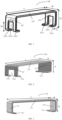
- FIGS. 1 to 3 are schematic structural diagrams of three exemplary strip radiation antennas provided by exemplary embodiments of the present disclosure.
- the strip radiation antenna 100 includes a first support section 101, a second support section 102, and a middle section 103, where the first support section 101 and the second support section 102 are located at two ends of the middle section 103 respectively, and both are bent toward a same side of the middle section 103.
- both the first support section 101 and the second support section 102 are bent toward a lower surface of the middle section 103, thus forming the strip radiation antenna 100 with a bench-like shape.
- the first support section 101 and the second support section 102 can be used to support the middle section 103, and a hollow structure is formed among the first support section 101, the second support section 102 and the middle section 103. Therefore, after the strip radiation antenna 100 is mounted on the PCB, there is a certain space between the middle section 103 and a surface of the PCB (e.g., the middle section 103 is not contact with the surface of the PCB).
- the first support section 101 and the second support section 102 can be bent by 90°(degrees) or close to 90°, so as to form a regular-shaped strip radiation antenna 100.
- a difference between the three is mainly due to the different number of pins.
- two first pins namely a pin 1011 and a pin 1012
- a first notch 1013 is formed between the two pins.
- two second pins namely a pin 1021 and a pin 1022, are formed at the end of the second support section 102, and a second notch 1023 is formed between the two pins.
- the antenna when viewed from the front of the strip radiation antenna 100, the antenna is axisymmetric, the first support section 101 and the second support section 102 are symmetrical with each other around a connecting line (see a dash line X0 shown in FIG. 4 ) between center points of two long sides of the middle section 103.
- one first pin namely a pin 1011
- two second pins namely a pin 1021 and a pin 1022
- a second notch 1023 is formed between the two pins.
- one first pin namely a pin 1011
- one second pin namely a pin 1021
- the first support section 101 and the second support section 102 of the strip radiation antenna 100 shown in FIG. 3 are also symmetrical with each other around the connecting line between the center points of the two long sides of the middle section 103.
- FIGS. 1 to 3 are only exemplary.
- one or more pins can be formed at the end of any support section of the strip radiation antenna 100, in the case of forming a plurality of pins, a corresponding notch (gap) can be formed between any two adjacent pins, and the present disclosure does not impose any limitation on the number of pins and notches.
- the microstrip composite antenna described in the present disclosure is a radio frequency antenna, which can be used to transmit or receive radio frequency signals in a specific frequency band (or frequency range).
- a radio frequency antenna As a key component of microstrip composite antenna, sizes of strip radiation antenna will affect an overall frequency band of the microstrip composite antenna, so it is necessary to design its sizes reasonably.
- the dimensions of the strip radiation antenna 100 mainly include a length L, a height H, and a width W.
- the specific dimension of the strip radiation antenna 100 can be reasonably set according to actual situations, e.g., the antenna's expected parameter specifications, production process accuracy, etc., and the specific values of its dimensions are not limited in the present disclosure.
- an RF signal frequency at this time is a resonant frequency of the RF antenna, also known as a resonant point.
- the microstrip composite antenna can work in a frequency band of 431 to 437 MHz (e.g., 434 ⁇ 3 MHz), the resonant frequency of the antenna is within this frequency band and as close as possible to 434 MHz.
- the signal attenuation of microstrip composite antenna is relatively small, which can ensure that the antenna has high gain when its resonant frequency is in the frequency band of 431 to 437 MHz (e.g., 434 MHz).
- a thickness of the strip radiation antenna also needs to be set reasonably.
- the thickness of the antenna can range from 0.2 to 1.0 mm, preferably, it can be 0.4 mm, 0.5 mm, 0.6 mm, etc.
- the pins formed at the end of the support sections of the strip radiation antenna shown in FIGS. 1 to 3 all use surface mounted technology (SMT), or, any of the above pins can also be direct-inserted pins/through hole leads.
- any or all of the first pin and the second pin can be surface mounted or directly inserted, e.g., each first pin can be surface mounted or directly inserted, and in the case of multiple first pins, some first pins can be surface mounted and the rest can be directly inserted (as shown in FIG. 1 , the pin 1011 can be surface mounted and the pin 1012 can be directly inserted).
- each second pin can be surface mounted or directly inserted.
- some second pins can be surface mounted and the rest can be directly inserted (as shown in FIG. 1 , the pin 1021 can be surface mounted and the pin 1022 can be directly inserted).
- the specific form of the pins of the strip radiation antenna should be reasonably set according to the space on the PCB, and the embodiments of the present disclosure do not limit it.
- the strip radiation antenna can be formed by stamping and/or bending a strip-shaped metal sheet to obtain the middle section, the first support section, and the second support section.
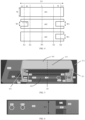
- FIG. 4 is a schematic diagram of a production process of a strip radiation antenna according to an exemplary embodiment.
- a distance from a left edge of the metal sheet to a dash line X1 and a distance from a right edge of the metal sheet to a dash line X4 are both L1, this length will become a pin length of a mounted pin of the strip radiation antenna 100 (L1 as shown in FIG. 1 ).
- a distance between the dash line X1 and a dash line X2, and a distance between the dash line X3 and a dash line X4 are both H, this length will become the height of the strip radiation antenna 100 (H as shown in FIGS. 1 to 3 ).
- a distance between the dash line X2 and the dash line X3 is L, this length will become the length of the middle section 103 of the strip radiation antenna 100 (L as shown in FIGS. 1 to 3 ), and W will become the width of the strip radiation antenna 100 (W as shown in FIGS. 1 to 3 ). Widths of the first support section 101, the second support section 102, and the middle section 103 are equal, all of which are W.
- a bending process (e.g., bending by 90°) can be carried out first along each of the dash line X1 and the dash line X4 from the two ends of the metal sheet 401 to a direction of a center of the metal sheet (e.g., a direction towards X0), and then the bending process can be continued along each the dash line X2 and the dash line X3 in that direction, so as to obtain the strip radiation antenna 100 shown in FIG. 3 .
- a metal sheet 402 can be obtained by cutting or stamping both ends of the metal sheet 401 (the two ends can be stamped separately or simultaneously), and notches are formed at original positions of the two stamped or cut away parts (these two parts are rectangles located at both ends of the metal sheet 401, a length of which is L1+H1 and a width of which is W1).
- a bending process (e.g., bending by 90°) can be carried out first along the dash line X1 and the dash line X4 from the two ends of the metal sheet 402 to a direction of a center of the metal sheet (e.g., a direction towards X0), and then the bending process can be continued along the dash line X2 and the dash line X3 in that direction, so as to obtain the strip radiation antenna 100 shown in FIG. 1 .
- a metal sheet 403 can be obtained by stamping or cutting only a right end of the metal sheet 401, and a notch is formed at an original position of the stamped or cut part.
- a bending process (e.g., bending by 90°) can be carried out first along the dash line X1 and the dash line X4 from the two ends of the metal sheet 403 to a direction of a center of the metal sheet (e.g., a direction towards X0), and then the bending process can be continued along the dash line X2 and the dash line X3 in that direction, so as to obtain the strip radiation antenna 100 shown in FIG. 2 .
- the first bending is used to form the first pin and the second pin
- the second bending is used to form the first support section 101 and the second support section 102.
- the strip radiation antennas shown in FIGS. 1 to 3 can be obtained from the strip-shaped metal sheet 401 shown in FIG. 4 .
- the material of the strip radiation antenna described in the present disclosure is metal.
- a metal conductor with excellent conductivity such as copper or copper alloy can be selected to process the strip-shaped metal sheet 401, and the strip radiation antenna can be moulded based on the metal sheet.
- an inner core of the strip radiation antenna can be made of non-conductive materials (such as ceramics and plastics), and then a metal conductor with uniform thickness can be formed on a surface of the inner core by electroplating or spraying, so as to obtain a finished strip radiation antenna.
- the metal material is used for conducting electricity, and the inner core can play a supporting role. This method can use less metal to make a lighter strip radiation antenna, thus further saving metal and helping to reduce the weight of the antenna.
- anti-rust materials can be coated on the surface of the antenna by spraying or baking paint to avoid the antenna from rusting, so that the antenna can be applied to harsh environments such as high humidity and high salt.
- the anti-rust materials should be selected as much as possible that are not suitable for absorbing radio frequency signals, so as to reduce signal attenuation and improve antenna gain.
- the shapes of the strip radiation antennas shown in FIGS. 1 to 3 are only exemplary, and the shapes of the strip radiation antennas, the number of pins, the types of pins, and other specifics can be reasonably set up or appropriately modified according to the actual situation in the solution practice, and the embodiments of the present disclosure do not limit this.
- the microstrip radiation line is printed in the PCB, such that the microstrip radiation line may be formed by a conductive copper foil printed in the PCB.
- Pads are printed at appropriate positions on the PCB so as to solder corresponding pins of the strip radiation antenna (the pads and pins are soldered to form a firmly connected soldering joint), thus forming an electrical connection between the microstrip radiation line and the strip radiation antenna to form a microstrip composite antenna.
- a substrate of the PCB described in the present disclosure can adopt any type of paper substrate, glass fiber cloth substrate, composite substrate (CEM series), laminated multilayer substrate and special material substrate (ceramic, metal core substrate, etc.).
- CEM series composite substrate
- ceramic metal core substrate
- dielectric constant ⁇ of substrates made of different materials is usually different, in order to reduce signal attenuation caused by absorption of RF signals transceived by the microstrip composite antenna, it is recommended to choose materials with dielectric constant ⁇ not greater than 5.5 as the substrate of PCB.
- the antenna Take the strip radiation antenna 100 shown in FIG. 1 as an example. If the antenna is soldered to the PCB 513, the antenna can be connected with the microstrip radiation line 500 printed on the PCB 513 to form a microstrip composite antenna. At this time, a relative position relationship between them can be seen in FIGS. 5 and 6 , and a structure of the microstrip composite antenna will be described using this as an example.
- the first pin is formed at the end of the first support section 101
- the second pin is formed at the end of the second support section 102.
- the number of the first pins can be one or more, where each of the first pins can be soldered to the PCB through a first pad at a corresponding position on the PCB.
- the number of the second pins can also be one or more, where each of the second pins can also be soldered to the PCB through a second pad at a corresponding position on the PCB, and the second pad can be connected to a ground plane of the PCB through a capacitor.
- the PCB may be printed with pad 506 and pad 507 as shown in FIG. 5 .
- the first pin 1011 of the strip radiation antenna 100 shown in FIG. 2 may be soldered to at least one of the two pads.
- a pad with a larger area can be set at the positions of the pad 506 and pad 507 (e.g., covering the current positions of the pad 506 and pad 507, and the shape of the pad can match a shape of a bottom surface of the first pin 1011 shown in FIG. 2 ), and the first pin 1011 can be soldered to the pad.
- a soldering method of the second pins (e.g., pins 1021 and 1022) of the strip radiation antenna 100 shown in FIG. 2 can be seen in FIG. 5 , and will not be described again.
- a pad with a larger area can be printed on the PCB corresponding to the pad 506 and pad 507 (e.g., covering the current positions of the pad 506 and pad 507, and the shape of the pad can match the shape of the bottom surface of the first pin 1011 shown in FIG. 3 ), and the first pin 1011 can be soldered to the pad.
- the strip radiation antenna 100 shown in FIG. 3 is soldered to the PCB 513, a pad with a larger area can be printed on the PCB corresponding to the pad 506 and pad 507 (e.g., covering the current positions of the pad 506 and pad 507, and the shape of the pad can match the shape of the bottom surface of the first pin 1011 shown in FIG. 3 ), and the first pin 1011 can be soldered to the pad.
- a pad with a larger area can be printed on the PCB 513 at the positions corresponding to the pad 504 and pad 505 (e.g., covering the current positions of the pad 504 and pad 505, and the shape of the pad can match the shape of the bottom surface of the second pin 1021 shown in FIG. 3 ), and the second pin 1021 can be soldered to the pad, which will not be described again.
- the number of the first pins or the second pins and the number of the corresponding pads can be reasonably set according to the actual conditions such as antenna performance and board space, and this is not limited by the embodiments of the present disclosure.
- corresponding to the four pins of the strip radiation antenna 100 there are corresponding pads set on the PCB 513, namely a first pad (pad 506 and pad 507) and a second pad (pad 504 and pad 505).
- the pin 1011 and the pin 1012 are soldered to the pad 506 and the pad 507, respectively, and the pin 1021 and the pin 1022 are soldered to the pad 504 and the pad 505, respectively.
- the first pad is connected to a second radiation line 502 printed in the PCB 513.
- the second pad is connected to the ground plane through a capacitor, such as the pad 504 is connected to the ground plane 510 through a capacitor 508 and the pad 505 is connected to the ground plane 510 through a capacitor 509.
- any pin of the strip radiation antenna 100 can be surface mounted or directly inserted. Since the first support section 101 and the second support section 102 are located at the two ends of the middle section 103, in order to shorten an overall length of the strip radiation antenna 100 and save the space of the PCB 513 as much as possible, any mounted pin of the mounting type may be bent towards another pin, that is, towards the center direction of the strip radiation antenna 100. For example, in the case that the first pin is surface mounted, it can be bent toward the second pin, and/or, in the case that the second pin is surface mounted, it can be bent toward the first pin. As shown in FIGS. 1 to 3 , each pin is bent toward the center direction of the middle section 103 (e.g., each pin is bent inward), so that the overall length L of the strip radiation antenna 100 is shorter (e.g., equal to the length of the middle section 103).
- any of the aforementioned pins can also be bent away from the other pin, which can increase a distance between the first pin and the second pin and reduce the soldering difficulty of the strip radiation antenna 100.
- the microstrip radiation line 500 printed within the PCB 513 includes two portions: a first radiation line 501 and a second radiation line 502.
- a first end 5011 of the first radiation line 501 is connected to a signal input and/or output point 512 of the keying modulation signal.
- the microstrip composite antenna receives a keying modulation signal modulated (or coded) by a signal modulation module through the signal input and/or output point 512 (at this time, the signal input and/or output point 512 is used as a signal input end of the microstrip composite antenna), the microstrip composite antenna can be used as a transmitting antenna to transmit the keying modulation signal (in a form of radio frequency signal) to the surrounding space, and the signal can be regarded as an output signal of the microstrip composite antenna.
- the microstrip composite antenna receives a keying modulation signal (which is essentially a radio frequency signal) modulated by a signal source and sent by other antennas from the surrounding space, it can output the signal to a signal demodulation module through the signal input and/or output point 512 (at this time, the signal input and/or output point 512 is used as a signal output end of the microstrip composite antenna), so that the module can demodulate (or decode) the keying modulation signal.
- the received keying modulation signal can be regarded as input signal of the microstrip composite antenna.
- the signal input and/or output point 512 to which the first end 5011 of the first radiation line 501 is connected can only be used as a signal input end of the microstrip composite antenna, can only be used as a signal output end of the microstrip composite antenna, or can be used as both a signal input end and a signal output end of the microstrip composite antenna.
- the microstrip composite antenna is a transceiver antenna, which can work in a simplex (only receiving or transmitting RF signals at the same time) or a duplex (receiving and transmitting RF signals at the same time) mode, and the specific connection mode and its working mode can be set as required, which is not limited by the embodiments of the present disclosure.
- the signal input and/or output point 512 can be connected to a signal input end or signal output end through a 50 ohm impedance line such as a coaxial cable signal line or a PCB line.
- the signal can have different types due to different modulation/demodulation algorithms corresponding to the keying modulation signal.
- the keying modulation signal may include at least one of the following: a frequency shift keying (FSK) signal, an amplitude shift keying (ASK) signal, or a phase shift keying (PSK) signal.
- FSK frequency shift keying
- ASK amplitude shift keying
- PSK phase shift keying
- the signal modulation module connected to the signal input end can use an ASK algorithm to encode the signal to be output, and output the encoded ASK signal to the first end 5011 of the first radiation line 501, so that the microstrip composite antenna can transmit the signal to the surrounding space as the radio frequency signal.
- the microstrip composite antenna can be integrated into an ASK transmitter.
- the signal demodulation module connected to the signal output end can use the ASK algorithm to decode the ASK signal received by the microstrip composite antenna, and output the decoded signal to a back end for further processing.
- the microstrip composite antenna can be integrated into an ASK receiver.
- the PCB 513 may include n layers for routing lines, 2 ⁇ n, and the PCB 513 is a multilayer board.
- the first radiation line 501 and the second radiation line 502 can be located at an i-th layer and a j-th layer in the n layers of lines respectively, where 1 ⁇ i ⁇ n, 1 ⁇ i ⁇ n, and i ⁇ j.
- the first radiation line 501 and the second radiation line 502 are located in different layers, so they can be connected across layers, for example, the first radiation line 501 can be connected to the second radiation line 502 across layers.
- the embodiments of the present disclosure do not limit relative sizes of i and j.
- the first radiation line 501 may be on the top (closer to the strip radiation antenna 100) or the second radiation line 502 may be on the top, which is not repeated here. Because the first radiation line 501 and the second radiation line 502 are located in different layers, it is necessary to realize cross-layer connection between them through a three-dimensional transmission line to effectively transmit the radio frequency signal. At this time, the microstrip radiation line 500 and the strip radiation antenna 100 can form a coplanar waveguide to achieve better signal coupling effect.
- the cross-layer connection can be realized in various ways, such as via (through hole), buried via, blind via and/or cross lines, which is not limited by the embodiments of the present disclosure.
- the first radiation line 501 and the second radiation line 502 can also be located in a same layer, such as a first layer in a multi-layer board or a same layer in a single-layer board (there is only one layer at this time).
- the first radiation line 501 and the second radiation line 502 can be kept parallel, for example, they are both strip-shaped and their axes are symmetrically distributed with a projection axis of an orthogonal projection of the middle section 103 on the PCB, e.g., the first radiation line 501 and the second radiation line 502 are located on both sides of the projection axis respectively.
- the microstrip radiation line 500 can also approximately form a coplanar waveguide with the strip radiation antenna 100, thereby achieving a certain degree of signal coupling.
- the first radiation line 501 can be located on a first layer below the middle section 103, and the second pin is soldered to the PCB 513 through a second pad located in the first layer.
- the signal input and/or output point 512 and the first end 5011 of the first radiation line 501 are located on both sides of the second support section 102 of the strip radiation antenna 100, respectively.
- the first end 5011 located on one side of the second support section 102 is connected to the signal input and/or output point 512 located on the other side of the second support section 102 through an extension wire 511.
- first layer below does not distinguish the front or back sides of the PCB, but only indicates that the strip radiation antenna 100 is soldered to a certain surface of the PCB, and the "first layer below” is the first layer counted down from the surface, such as a top layer or a bottom layer of the PCB.
- the extension wire 511 can be laid out in various ways.
- the extension wire 511 is connected to the first end 5011 bypassing the second pad in the first layer. If the strip radiation antenna 100 shown in FIG. 5 is replaced by the strip radiation antenna 100 shown in FIG. 3 (the antenna has only one second pin 1021), the extension wire 511 can bypass the pad corresponding to the second pin 1021 in the first layer and connect to the first end 5011. Or, as shown in FIG. 5 , if the ground plane 510 of the first layer does not surround the signal input and/or output point 512, the extension wire 511 can be connected to the first end 5011 by bypassing the pad 504 (e.g., routing from the outside of the pad 504) or pad 505 (e.g., routing from the outside of the pad 505) in the first layer.
- the pad 504 e.g., routing from the outside of the pad 504
- pad 505 e.g., routing from the outside of the pad 505
- a notch 1023 (the aforementioned second notch 1023) can also be set at the end of the second support section 102, and at this time, the extension wire 511 can pass under the notch 1023.
- FIG.5 please refer to FIG.5 .
- the first notch 1013 is formed at the end of the first support section of the strip radiation antenna 100 shown in FIG. 5 .
- These two notches can ensure that the radio frequency signal emitted by the strip radiation antenna 100 are distributed as symmetrically and evenly as possible in the surrounding space, which is helpful to improve the coverage of antenna signal.
- the end of the second support section 102 may form two symmetrical second pins, such as pin 1021 and pin 1022, centered on the notch 1023.
- Each of the two second pins may connect to the ground plane 510 of the PCB 513 through at least one capacitor.
- the pin 1021 is connected to the ground plane 510 through the capacitor 508.
- the pin 1022 can also be connected to the ground plane 510 in series or in parallel through two capacitors 509 and 509' (not shown in FIG. 5 ).
- one of the two second pins can be connected to the ground plane 510 of the PCB 513 through at least one capacitor, while the other second pin is vacant.
- an adjustable capacitor can be connected between the second pad and the ground plane 510, so as to adjust the resonant frequency of the antenna more accurately by adjusting the capacitance value of the adjustable capacitor.
- a width of the notch 1023 should be not less than 1.2 times a width of the extension wire 511. As shown in FIG. 5 , a width W1 of a notch between the pin 1021 and the pin 1022 (i.e., the second notch 1023) should be greater than or equal to 1.2 times the width of the extension wire 511. In addition, considering that the width of each position of the extension wire 511 can be the same or different, the width W1 of the notch 1023 should be at least 1.2 times greater than or equal to the width of the part of the extension wire 511 between the pin 1021 and the pin 1022.
- a second end 5012 of the first radiation line 501 is connected to the second radiation line 502, and the second radiation line 502 is further connected to the ground plane of the PCB 513.
- the first radiation line 501 and the second radiation line 502 are respectively located in the i-th and j-th layers as an example.
- the second end 5012 located in the i-th layer (such as the first layer) is connected to the second radiation line 502 located in the j-th layer (such as the second layer) through a via (the j-th layer can refer to FIG. 6 ).
- the second radiation line 502 can be connected to the ground plane 602 of the j-th layer through a bridge connection line 601. It is also possible to directly extend the second radiation line 502 to connect with the ground plane 602 without providing the bridge connection line 601.
- ground plane 510 shown in FIG. 5 located at the i-th layer
- the ground plane 602 shown in FIG. 6 located at the j-th layer
- the ground planes of each layer can be connected with each other to achieve the same zero potential inside the entire PCB 513, avoiding the phenomenon of "virtual ground”. Therefore, the ground plane 510 and the ground plane 610 can be regarded as the same ground plane, which is the ground plane GND of the PCB.
- the strip radiation antenna 100 is located above the microstrip radiation line 500, and at least one of the first radiation line 501 or the second radiation line 502 is parallel to the middle section 103 of the strip radiation antenna 100.
- the central axes of the first radiation line 501 and the second radiation line 502 are both parallel to the central axis of the middle section 103 (i.e., the central axes of all three are coplanar), while the second radiation line 502 is located below the first radiation line 501 and further away from a longitudinal direction of the strip radiation antenna 100.
- a length of the first radiation line 501 is not less than half of a length of the middle section 103.
- an orthographic projection of the second end 5012 of the first radiation line 501 on the middle section 103 is located on the side of the middle section 103 close to the first support section 101.
- the dash line X0 indicates a center position of the middle section 103 (in the direction of the length L), and the second end 5012 is located between the dash line X0 and the first support section 101 (i.e., to the right of the broken line X0).
- a ratio of a width W2 of the second radiation line 502 to a width W of the strip radiation antenna 100 should range from 0.8 to 1.2, that is, a difference between W2 and W should not exceed 20% of W.
- the W2 should be equal to the W, and at this time, a signal coupling degree between the second radiation line 502 and the strip radiation antenna 100 is better.
- the strip radiation antenna in order to reduce interference caused by the ground plane to the radio frequency signal received and transmitted by the strip radiation antenna (such as absorbing signal), the strip radiation antenna should be located as far away from the ground plane as possible. For example, if a long side of an orthogonal projection of the strip radiation antenna 100 on the PCB 513 is parallel to at least one edge of the ground plane 510, a distance between the long side and the edge should be not less than 6 mm. As shown in FIG. 7 , a long side 701 of the orthogonal projection of the strip radiation antenna 100 on the PCB 513 is parallel to an edge 702 of the ground plane 410. At this time, the distance S between the long side 701 and the edge 702 should be not less than 6 mm to minimize the possible interference of the ground plane 410 on the working process of the strip radiation antenna 100.
- a signal processor/signal processing module can also be integrated in the PCB 513 where the microstrip composite antenna is located, and the module can be connected to the signal input and/or output point 512.
- the signal processing module can be configured to demodulate keying modulation signals received through the microstrip composite antenna and/or to output modulated keying modulation signals to the microstrip composite antenna, so as to transmit the signals to the surrounding space through the antenna.
- the signal processing module modulates or demodulates the keying modulation signals
- corresponding keying algorithms should be used, such as obtaining the ASK signal by modulating or demodulating the ASK signal through the ASK algorithm, obtaining the FSK signal by modulating or demodulating the FSK signal through the FSK algorithm, obtaining the PSK signal by modulating the PSK algorithm or demodulating the PSK signal through the PSK algorithm, etc.
- the signal processing module demodulates the keying modulation signal it is implemented as the aforementioned signal demodulation module.
- the signal processing module modulates the keying modulation signal it is implemented as the aforementioned signal modulation module.
- the aforementioned signal demodulation module and signal modulation module may be functional units integrated in the signal processing module.
- a control module such as microcontroller unit, MCU
- an interface circuit (not shown in the figures) can be integrated in the PCB 513, and the interface circuit can integrate relevant interfaces such as power supply and communication, so as to supply power to the PCB 513 and establish communication with other devices (or functional modules of other devices) for data interaction.
- the microstrip composite antenna and related functional modules described in the present disclosure can be highly integrated on the PCB 513, thus further realizing miniaturization and integration of functional modules.
- the strip radiation antenna of this solution establishes a connection with the microstrip radiation lines printed on the PCB through the pins at both ends, and together form a microstrip composite antenna. Because the first end of the first radiation line is connected to the signal input and/or output point of the keying modulation signal, the microstrip composite antenna can be configured to receive and/or send the keying modulation signal (such as ASK, FSK, etc.).
- the keying modulation signal such as ASK, FSK, etc.
- the size of the strip radiation antenna is not limited by ⁇ /4 , so the size of both the strip radiation antenna and the microstrip composite antenna is significantly reduced compared with the conventional bracket antenna.
- the microstrip composite antenna can work stably at the expected resonant frequency and has a high antenna gain through the mutual cooperation of the microstrip radiation line and the strip radiation antenna. For example, the gain at the measured resonant frequency of 434.4 MHz is about -1.9 dBi, which is much higher than that of a spiral antenna of similar size.
- the microstrip composite antenna can effectively meet the requirements of miniaturization and high gain at the same time.
- the strip radiation antenna can be made of strip metal with strong rigidity, so it is not easy to deform, thus ensuring the microstrip composite antenna to work stably at or near the resonant frequency.
- the strip radiation antenna is firmly soldered to the PCB through pins, the strip radiation antenna is provided with good anti-vibration properties, higher structural stability and signal stability.
- microstrip composite antenna is introduced, and its actual performance is explained with experimental data.
- Connect a first end to a signal output end via a 50 ohm coaxial cable that is, use the antenna as a receiving antenna
- draw a Smith chart through a vector network analyzer
- observe positions of Mark points at a set frequency such as 434 MHz
- the resonant frequency of the microstrip composite antenna is changed by adjusting the capacitor values of capacitors 508 and 509.
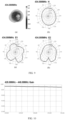
- FIG. 9 (b) As shown in measured diagrams of radiation directions of radio frequency signals in FIG. 9 , it can be seen from FIG. 9 (b) , (c) and (d) that when the microstrip composite antenna works at 434.00 Mhz, its maximum gain on a H-plane (e.g., xy-plane) is located near 210° direction, on a E1-plane (e.g., xz-plane) is located near the 210° direction, and on a E2-plane (e.g., yz-plane) is located near 135° direction.
- an overall maximum gain of the microstrip composite antenna is -1.9 dBi
- a measured gain diagram shown in FIG. 10 shows a variation curve of antenna gain in the frequency band of 420.00 to 440.00 MHz, which is also proved by a gain value around 434.00 MHz.
- a comparative test was conducted on the signal distance between the aforementioned microstrip composite antenna in the solution and a similarly sized spiral antenna, where the two antennas are configured to receive radio frequency signals (e.g., carrying tire pressure information collected by a sensor) sent by the TPMS sensor.
- the test conditions are as follows.
- the RF communication rate is set to 19.2 kbps
- FSK receiving sensitivity is set to -102 dBm
- signal power of the TPMS sensor is 5 dBm.
- the sensor is placed in a fixed position (coordinate zero) as a signal source to start the test, and test results can be seen in FIG. 11 . As shown in FIG.
- a farthest receiving distance of the microstrip composite antenna in this solution is about 50 m, and the farthest receiving distance in eight directions around the signal source is relatively uniform, generally within 49 to 53m.
- a farthest receiving distance of spiral antennas with similar dimensions is generally about 40 m. It can be seen that the farthest signal receiving distance of the microstrip composite antenna described in the present disclosure is about 20% higher than that of the similar size spiral antenna.
- the performance parameters of the microstrip composite antenna described in the present disclosure such as the gain and the farthest signal receiving distance, are excellent, and the performance is obviously improved compared with that of the spiral antenna.
- the present disclosure further proposes an integrated circuit board with highly integrated components and functions.
- the integrated circuit board includes a control module, a signal processing module, an interface module, and the microstrip composite antenna according to any of the previous embodiments, where a first end of the microstrip radiation line in the microstrip composite antenna is connected with the signal processing module.
- the integrated circuit board 1200 includes a control module 1201, a signal processing module 1202, an interface module 1203 and a microstrip composite antenna 1204.
- the control module 1201 is configured to control a normal operation of the integrated circuit board 1200.
- the signal processing module 1202 is configured to demodulate the keying modulation signal received through the microstrip composite antenna 1204 and/or for transmit the modulated keying modulation signal to the surrounding space through the microstrip composite antenna 1204.
- the interface module 1203 can integrate various interfaces such as power supply interface and communication interface, and through this module, the power and communication connection between the integrated circuit board 1200 and other devices can be realized.
- a microstrip composite antenna 1302 is mounted on an integrated circuit board 1301. Using a vernier caliper 1303 to measure the size of the integrated circuit board 1301, it can be seen from readings 1304 in (a) and (b) that the circuit board is about 30mm in length and 42mm in width.
- an integrated circuit board equipped with a miniaturized and high-gain microstrip composite antenna is only 30mm*42mm, which is significantly smaller than that of a circuit board equipped with a conventional antenna (such as a bracket antenna), thus realizing the miniaturization of the circuit board (based on a small-sized microstrip composite antenna).
- a conventional antenna such as a bracket antenna
- the microstrip composite antenna described in the present disclosure can be assembled in a vehicle as an independent antenna, or the integrated circuit board described in the present disclosure can also be integrated in a vehicle as a signal processing device integrated with an antenna module.
- the present disclosure further proposes a vehicle, which is equipped with a microstrip composite antenna as described in any of the previous embodiments, or an integrated circuit board as described in any of the previous embodiments.
- the microstrip composite antenna or integrated circuit board assembled in the vehicle can be configured to receive tire pressure, temperature, humidity and other signals emitted by tire pressure sensors (or TPMS sensors) installed in the vehicle tires, and submit them to a vehicle's computer system after appropriate processing for easy archiving and/or display to users for viewing.
- tire pressure sensors or TPMS sensors
Landscapes
- Waveguide Aerials (AREA)
Applications Claiming Priority (1)
| Application Number | Priority Date | Filing Date | Title |
|---|---|---|---|
| PCT/CN2023/117797 WO2025050395A1 (fr) | 2023-09-08 | 2023-09-08 | Antenne composite microruban destinée à recevoir et/ou émettre un signal de modulation |
Publications (2)
| Publication Number | Publication Date |
|---|---|
| EP4546565A1 true EP4546565A1 (fr) | 2025-04-30 |
| EP4546565A4 EP4546565A4 (fr) | 2025-04-30 |
Family
ID=94922821
Family Applications (1)
| Application Number | Title | Priority Date | Filing Date |
|---|---|---|---|
| EP23901756.9A Pending EP4546565A4 (fr) | 2023-09-08 | 2023-09-08 | Antenne composite microruban destinée à recevoir et/ou émettre un signal de modulation |
Country Status (2)
| Country | Link |
|---|---|
| EP (1) | EP4546565A4 (fr) |
| WO (1) | WO2025050395A1 (fr) |
Family Cites Families (7)
| Publication number | Priority date | Publication date | Assignee | Title |
|---|---|---|---|---|
| TWI411161B (zh) * | 2009-08-06 | 2013-10-01 | Univ Nat Defense | A five - frequency antenna for portable electronic devices |
| EP2458679B1 (fr) * | 2009-09-10 | 2016-07-27 | Delphi Delco Electronics Europe GmbH | Antenne pour la réception de signaux satellite circulaires polarisés |
| TWI389389B (zh) * | 2009-09-21 | 2013-03-11 | Yuanchih Lin | 圓極化平板天線 |
| JP5353609B2 (ja) * | 2009-09-29 | 2013-11-27 | 株式会社日本自動車部品総合研究所 | アンテナ装置 |
| IT1400110B1 (it) * | 2010-05-21 | 2013-05-17 | S Di G Moiraghi & C Soc Sa | Antenna planare compatta. |
| DE102020211228A1 (de) * | 2020-09-08 | 2022-03-10 | Robert Bosch Gesellschaft mit beschränkter Haftung | Sendevorrichtung sowie Verfahren zum Herstellen einer Sendevorrichtung |
| WO2023136742A1 (fr) * | 2022-01-14 | 2023-07-20 | Limited Liability Company "Topcon Positioning Systems" | Antenne à plaque à double alimentation avec ports isolés |
-
2023
- 2023-09-08 EP EP23901756.9A patent/EP4546565A4/fr active Pending
- 2023-09-08 WO PCT/CN2023/117797 patent/WO2025050395A1/fr active Pending
Also Published As
| Publication number | Publication date |
|---|---|
| WO2025050395A1 (fr) | 2025-03-13 |
| EP4546565A4 (fr) | 2025-04-30 |
Similar Documents
| Publication | Publication Date | Title |
|---|---|---|
| CA2200675C (fr) | Structure d'antenne a circuits imprimes utilisee pour la transmission de donnees sans fil | |
| TWI578618B (zh) | 開槽天線及具有該開槽天線的無線通訊裝置 | |
| US20110309993A1 (en) | Small-size printed circuit board-printed meander line inverted-f antenna for radio frequency integrated circuits | |
| US20110309985A1 (en) | Wideband printed circuit board-printed antenna for radio frequency front end circuit | |
| US8547184B2 (en) | High-frequency coupler and communication device | |
| CN110994178B (zh) | 一种天线结构及电子设备 | |
| US20110199272A1 (en) | Field-confined printed circuit board-printed antenna for radio frequency front end integrated circuits | |
| CN109075450A (zh) | 天线 | |
| US10938097B2 (en) | PCB antenna | |
| JP2009060403A (ja) | 無線装置および無線装置が備えるアンテナ | |
| TW201015782A (en) | Multi-frequency antenna and an electronic device having the multi-frequency antenna thereof | |
| CN103794868A (zh) | 天线组件 | |
| CN111430863A (zh) | 传输线以及终端设备 | |
| US9640854B2 (en) | Wireless communication device | |
| US6297779B1 (en) | Antenna module for portable computer | |
| TWI566466B (zh) | 天線組件及具有該天線組件之無線通訊裝置 | |
| CN216597978U (zh) | 一种单极性板载天线及pcb板 | |
| CN215418598U (zh) | 天线和带金属组件的电子装置 | |
| CN220830108U (zh) | 用于接收和/或发送键控调制信号的微带复合天线、集成电路板和车辆 | |
| JP2014003608A (ja) | アンテナモジュール及びこのアンテナモジュールを備えた無線通信装置 | |
| WO2025050395A1 (fr) | Antenne composite microruban destinée à recevoir et/ou émettre un signal de modulation | |
| JP5944363B2 (ja) | アンテナモジュール | |
| EP1801987A1 (fr) | Module de radiocommunication et dispositif de radiocommunication | |
| CN114094330A (zh) | 一种设备及其天线 | |
| CN216597983U (zh) | 双频合一天线 |
Legal Events
| Date | Code | Title | Description |
|---|---|---|---|
| STAA | Information on the status of an ep patent application or granted ep patent |
Free format text: STATUS: UNKNOWN |
|
| STAA | Information on the status of an ep patent application or granted ep patent |
Free format text: STATUS: THE INTERNATIONAL PUBLICATION HAS BEEN MADE |
|
| PUAI | Public reference made under article 153(3) epc to a published international application that has entered the european phase |
Free format text: ORIGINAL CODE: 0009012 |
|
| STAA | Information on the status of an ep patent application or granted ep patent |
Free format text: STATUS: REQUEST FOR EXAMINATION WAS MADE |
|
| 17P | Request for examination filed |
Effective date: 20240620 |
|
| A4 | Supplementary search report drawn up and despatched |
Effective date: 20250213 |
|
| AK | Designated contracting states |
Kind code of ref document: A1 Designated state(s): AL AT BE BG CH CY CZ DE DK EE ES FI FR GB GR HR HU IE IS IT LI LT LU LV MC ME MK MT NL NO PL PT RO RS SE SI SK SM TR |