EP4550663A1 - Verteilter programmierbarer verstärker - Google Patents
Verteilter programmierbarer verstärker Download PDFInfo
- Publication number
- EP4550663A1 EP4550663A1 EP24204136.6A EP24204136A EP4550663A1 EP 4550663 A1 EP4550663 A1 EP 4550663A1 EP 24204136 A EP24204136 A EP 24204136A EP 4550663 A1 EP4550663 A1 EP 4550663A1
- Authority
- EP
- European Patent Office
- Prior art keywords
- terminal
- impedance
- transmission line
- resistance
- signal
- Prior art date
- Legal status (The legal status is an assumption and is not a legal conclusion. Google has not performed a legal analysis and makes no representation as to the accuracy of the status listed.)
- Pending
Links
Images




Classifications
-
- H—ELECTRICITY
- H03—ELECTRONIC CIRCUITRY
- H03F—AMPLIFIERS
- H03F3/00—Amplifiers with only discharge tubes or only semiconductor devices as amplifying elements
- H03F3/189—High-frequency amplifiers, e.g. radio frequency amplifiers
- H03F3/19—High-frequency amplifiers, e.g. radio frequency amplifiers with semiconductor devices only
- H03F3/195—High-frequency amplifiers, e.g. radio frequency amplifiers with semiconductor devices only in integrated circuits
-
- H—ELECTRICITY
- H03—ELECTRONIC CIRCUITRY
- H03F—AMPLIFIERS
- H03F3/00—Amplifiers with only discharge tubes or only semiconductor devices as amplifying elements
- H03F3/60—Amplifiers in which coupling networks have distributed constants, e.g. with waveguide resonators
- H03F3/605—Distributed amplifiers
-
- H—ELECTRICITY
- H03—ELECTRONIC CIRCUITRY
- H03F—AMPLIFIERS
- H03F1/00—Details of amplifiers with only discharge tubes, only semiconductor devices or only unspecified devices as amplifying elements
- H03F1/42—Modifications of amplifiers to extend the bandwidth
- H03F1/48—Modifications of amplifiers to extend the bandwidth of aperiodic amplifiers
-
- H—ELECTRICITY
- H03—ELECTRONIC CIRCUITRY
- H03F—AMPLIFIERS
- H03F1/00—Details of amplifiers with only discharge tubes, only semiconductor devices or only unspecified devices as amplifying elements
- H03F1/56—Modifications of input or output impedances, not otherwise provided for
- H03F1/565—Modifications of input or output impedances, not otherwise provided for using inductive elements
-
- H—ELECTRICITY
- H03—ELECTRONIC CIRCUITRY
- H03G—CONTROL OF AMPLIFICATION
- H03G3/00—Gain control in amplifiers or frequency changers
- H03G3/20—Automatic control
-
- H—ELECTRICITY
- H03—ELECTRONIC CIRCUITRY
- H03G—CONTROL OF AMPLIFICATION
- H03G3/00—Gain control in amplifiers or frequency changers
- H03G3/20—Automatic control
- H03G3/30—Automatic control in amplifiers having semiconductor devices
- H03G3/3052—Automatic control in amplifiers having semiconductor devices in bandpass amplifiers (H.F. or I.F.) or in frequency-changers used in a (super)heterodyne receiver
- H03G3/3078—Circuits generating control signals for digitally modulated signals
-
- H—ELECTRICITY
- H03—ELECTRONIC CIRCUITRY
- H03H—IMPEDANCE NETWORKS, e.g. RESONANT CIRCUITS; RESONATORS
- H03H7/00—Multiple-port networks comprising only passive electrical elements as network components
- H03H7/38—Impedance-matching networks
- H03H7/383—Impedance-matching networks comprising distributed impedance elements together with lumped impedance elements
-
- H—ELECTRICITY
- H04—ELECTRIC COMMUNICATION TECHNIQUE
- H04L—TRANSMISSION OF DIGITAL INFORMATION, e.g. TELEGRAPHIC COMMUNICATION
- H04L25/00—Baseband systems
- H04L25/02—Details ; arrangements for supplying electrical power along data transmission lines
- H04L25/0264—Arrangements for coupling to transmission lines
- H04L25/0278—Arrangements for impedance matching
-
- H—ELECTRICITY
- H03—ELECTRONIC CIRCUITRY
- H03F—AMPLIFIERS
- H03F2200/00—Indexing scheme relating to amplifiers
- H03F2200/255—Amplifier input adaptation especially for transmission line coupling purposes, e.g. impedance adaptation
-
- H—ELECTRICITY
- H03—ELECTRONIC CIRCUITRY
- H03F—AMPLIFIERS
- H03F2200/00—Indexing scheme relating to amplifiers
- H03F2200/451—Indexing scheme relating to amplifiers the amplifier being a radio frequency amplifier
-
- H—ELECTRICITY
- H03—ELECTRONIC CIRCUITRY
- H03G—CONTROL OF AMPLIFICATION
- H03G2201/00—Indexing scheme relating to subclass H03G
- H03G2201/10—Gain control characterised by the type of controlled element
- H03G2201/103—Gain control characterised by the type of controlled element being an amplifying element
Definitions
- the present disclosure is directed to devices for high-speed electrical/optical communications.
- PGAs take in high-speed signals that may vary significantly in amplitude and amplify/attenuate them to a constant amplitude that is amenable to sub-stream circuits to maintain signal integrity in the face of noise and signal loss, ensuring that data can be accurately transmitted and received.
- an apparatus comprising:
- the second transmission line comprises one or more inductor-capacitor segments coupled in series, wherein the each inductor in the one or more inductor-capacitor segments is arranged in series in the second transmission line and each capacitor of the one or more inductor-capacitor segments is arranged in parallel between the second transmission line and the ground to configure the second transmission line with an impedance-matched termination.
- the third circuit is configured to have a third impedance for the second signal from the third terminal downstream, the third impedance being equal to the second impedance.
- the second circuit is configured to have a fourth impedance for the first signal from the second terminal downstream, the fourth impedance being equal to a parallel combination of the second resistance and a sum of the third resistance plus the third impedance.
- the second resistance and the third resistance are adjustable to set the fourth impedance equal to the first impedance to configure the first transmission line with an impedance-matched termination at the second terminal.
- the first circuit is configured to have a fifth impedance for the first signal from the first terminal downstream, the fifth impedance being equal to the first impedance.
- the first circuit is configured to transmit the first signal from the first terminal to the second terminal with a return loss of less than -10dB across a full bandwidth of 55GHz or higher.
- the gain is based on a ratio of the second impedance over a sum of the second impedance and the third resistance.
- the gain has a range of at least 11dB across a full bandwidth of 55GHz or higher.
- the third resistor comprises an array of resistors with different resistances controlled by respective switches.
- the switch comprises a transistor with a gate terminal coupled to a first terminal of a fifth resistor with a resistance greater than 100 KOhm, the fifth resistor having a second terminal coupled to a control signal.
- the first transmission line comprises one or more inductor-capacitor segments coupled in series, wherein each inductor in the one or more inductor-capacitor segments is arranged in series in the first transmission line and each capacitor of the one or more inductor-capacitor segments is arranged in parallel between the first transmission line and the ground.
- the apparatus further comprises at least a fourth circuit comprising a transistor coupled to the second transmission line to provide an output signal based on the second signal at the third terminal.
- the first transmission line comprises one or more inductor-capacitor segments with each inductor being arranged in series and each capacitor being arranged in parallel, the one or more inductor-capacitor segments being characterized by a first impedance that is equal to the first resistance.
- the second transmission line comprises one or more inductor-capacitor segments with each inductor being arranged in series and each capacitor being arranged in parallel, the one or more inductor-capacitor segments being characterized by a second impedance that is equal to the fourth resistance.
- the second transmission line is configured to have a third impedance for the second signal from the third terminal downstream, the third impedance being equal to the second impedance attributed to the second impedance-matched termination across a full bandwidth of 55GHz or higher.
- the gain is approximately uniform across a full bandwidth of 55GHz or higher and has a tunable range of at least 11dB based on a ratio of the second impedance over a sum of the second impedance and the third resistance, wherein the third resistance is adjustable, and the second impedance is equal to the fourth resistance.
- a wideband programmable gain amplifier including a distributed input network configured to set impedance-matched input coupling and impedance-matched termination to transmit signal with low return loss in large bandwidth.
- the apparatus also includes a resistor-based network embedded in the distributed input network to achieve programmable gain for the signal with a wide gain range and uniform gain tunning across the large bandwidth. It is important to note that there are other alternative embodiments as well.
- a layer can be a single layer or include multiple layers.
- a conductive layer may comprise multiple different conductive materials or multiple layers of different conductive materials
- a dielectric layer may comprise multiple dielectric materials or multiple layers of dielectric materials.
- left, right, front, back, top, bottom, forward, reverse, clockwise and counterclockwise are used for purposes of explanation only and are not limited to any fixed direction or orientation. Rather, they are used merely to indicate relative locations and/or directions between various parts of an object and/or components.
- the phrase "at least one of” preceding a series of items, with the term “and” or “or” to separate any of the items, modifies the list as a whole, rather than each member of the list (i.e., each item).
- the phrase "at least one of” does not require selection of at least one of each item listed; rather, the phrase allows a meaning that includes at least one of any one of the items, and/or at least one of any combination of the items.
- the phrases “at least one of A, B, and C" or “at least one of A, B, or C” each refer to only A, only B, or only C; and/or any combination of A, B, and C. In instances where it is intended that a selection be of "at least one of each of A, B, and C," or alternatively, "at least one of A, at least one of B, and at least one of C,” it is expressly described as such.
- the apparatus also includes a first circuit.
- the first circuit may include a first transmission line starting from a first terminal and terminating at a second terminal, the first terminal being coupled to a source to receive a first signal, the source being coupled to ground via a first resistor characterized by a first resistance, the first transmission line being characterized by a first impedance being equal to the first resistance.
- the apparatus also includes a second circuit.
- the second circuit may include at least a second resistor characterized by a second resistance and a third resistor characterized by a third resistance, the second resistor being coupled between the second terminal and ground, the third resistor being coupled between the second terminal and a third terminal, the second circuit being configured to transmit the first signal from the first terminal to the second terminal and provide a gain to a second signal at the third terminal over the first signal.
- the apparatus also includes a third circuit.
- the third circuit may include a second transmission line starting from the third terminal and terminating with a fourth resistor, the fourth resistor being grounded and characterized by a fourth resistance, the second transmission line being characterized by a second impedance being equal to the fourth resistance.
- Implementations may include one or more of the following features.
- the apparatus where the second transmission line includes one or more inductor-capacitor segments coupled in series, where the each inductor in the one or more inductor-capacitor segments is arranged in series in the second transmission line and each capacitor of the one or more inductor-capacitor segments is arranged in parallel between the second transmission line and the ground to configure the second transmission line with an impedance-matched termination.
- the third circuit is configured to have a third impedance for the second signal from the third terminal downstream, the third impedance being equal to the second impedance.
- the second circuit is configured to have a fourth impedance for the first signal from the second terminal downstream, the fourth impedance being equal to a parallel combination of the second resistance and a sum of the third resistance plus the third impedance.
- the second resistance and the third resistance are adjustable to set the fourth impedance equal to the first impedance to configure the first line with an impedance-matched termination at the second terminal.
- the first circuit is configured to have a fifth impedance for the first signal from the first terminal downstream, the fifth impedance being equal to the first impedance.
- the first circuit is configured to transmit the first signal from the first terminal to the second terminal with a return loss at least less than -10dB across a full bandwidth of 55GHz or higher.
- the gain is based on a ratio of the second impedance over a sum of the second impedance and the third resistance.
- the gain has a tunable range of at least 11dB across a full bandwidth of 55GHz or higher.
- the gain is approximately uniform within 2dB across a full bandwidth of 55GHz or higher.
- the third resistor may include an array of resistors with different resistances controlled by respective switches.
- the switch may include a transistor with a gate terminal coupled to a first terminal of a fifth resistor with a resistance greater than 100 Kohm, the fifth resistor having a second terminal coupled to a control signal.
- the first line may include one or more inductor-capacitor segments coupled in series, where each inductor in the one or more inductor-capacitor segments is arranged in series in the first line and each capacitor of the one or more inductor-capacitor segments is arranged in parallel between the first line and the ground.
- the apparatus may include at least a fourth circuit.
- the fourth circuit may include a transistor coupled to the second transmission line to provide an output signal based on the second signal at the third terminal.
- the apparatus also includes a first transmission line disposed from a first terminal to a second terminal, the first terminal being coupled to a source to receive a first signal, the source being coupled to ground via a first resistor characterized by a first resistance, the first transmission line being configured to transmit the first signal from the first terminal to the second terminal.
- the apparatus also includes a second resistor characterized by a second resistance coupled between the second terminal and ground.
- the apparatus also includes a third resistor characterized by a third resistance coupled between the second terminal and a third terminal, the second resistance and the third resistance being adjustable to configure the first transmission line with a first impedance-matched termination at the second terminal and to provide a second signal at the third terminal with a gain over the first signal at the second terminal.
- the apparatus also includes a second transmission line disposed from the third terminal to a fourth resistor, the fourth resistor being coupled to the ground and characterized by a fourth resistance, the second transmission line being configured to have a second impedance-matched termination for transmitting the second signal.
- Implementations may include one or more of the following features.
- the apparatus where the first transmission line may include one or more inductor-capacitor segments with each inductor being arranged in series and each capacitor being arranged in parallel, the one or more inductor-capacitor segments being characterized by a first impedance that is equal to the first resistance.
- the second transmission line may include one or more inductor-capacitor segments with each inductor being arranged in series and each capacitor being arranged in parallel, the one or more inductor-capacitor segments being characterized by a second impedance that is equal to the fourth resistance.
- the second transmission line is configured to have a third impedance for the second signal from the third terminal downstream, the third impedance being equal to the second impedance.
- the apparatus being configured to have a fourth impedance for the first signal from the second terminal downstream based on a product of the second resistance and a sum of the third resistance plus the third impedance dividing a sum of the second resistance plus the third resistance plus the third impedance, the fourth impedance being equal to the first impedance attributed to the first impedance-matched termination at the second terminal.
- the gain is approximately uniform across a full bandwidth of 55GHz or higher and has a tunable range of at least 11dB based on a ratio of the second impedance over a sum of the second impedance and the third resistance, where the third resistance is adjustable, and the second impedance is equal to the fourth resistance.
- PGAs Programmable Gain Amplifiers
- PGAs can be used to amplify the input signal before serialization, ensuring that it can be accurately received and deserialized at the other end.
- PGAs can be used in both the transmitting and receiving ends.
- a PGA can amplify the electrical signal before it is converted into an optical signal, ensuring that it can travel longer distances.
- a PGA can amplify the received signal before it is converted back into an electrical signal, ensuring that it can be accurately interpreted.
- the distributed input network 101 designed for the gain amplifier may use an artificial transmission line, usually made up of cascaded inductors and capacitors, to handle the signal amplification/attenuation by emulating ideal transmission line characteristics.
- an artificial transmission line in the context of subject technology refers to a structured network of passive components, typically inductors and capacitors, arranged in a way that emulates the electrical properties and behavior of a traditional transmission line. Unlike natural transmission lines, these artificial constructs allow designers to fine-tune specific electrical characteristics, providing greater control over signal integrity, impedance characteristics, and other critical parameters.
- the artificial transmission line can be implemented as a series of cascaded inductor-capacitor (LC) segments or other topologies to achieve the desired transmission line characteristics may have multiple sections.
- LC cascaded inductor-capacitor
- an input coupling circuit 111 is situated at the start of the artificial transmission line, responsible for matching the impedance of the signal source to the artificial transmission line.
- the output coupling circuit 112 is located at the end of the artificial transmission line of the distributed network, performing the reverse function of the input coupling, matching the transmission line's impedance to the load or the next stage.
- a gain circuit 120 representing at least one of the multiple gain stages distributed along the artificial transmission line, is disposed between the input coupling circuit 111 and the output coupling circuit 112, responsible for the amplification/attenuation of the signal as it traverses the line.
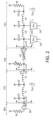
- FIG. 2 is a simplified circuit diagram of a distributed programmable gain amplifier according to an embodiment of the subject technology. This diagram is merely an example, which should not unduly limit the scope of the claims. One of ordinary skill in the art would recognize many variations, alternatives, and modifications.
- a distributed gain amplifier is provided by implementing a distributed input network for achieving large bandwidth and an embedded resistor network for achieving flexible gain adjustment mechanism and linear performance over a wide frequency range. As shown in FIG. 2 , the distributed input network is made up of one artificial transmission line configured to couple to a signal source 20 at an input stage 201 to receive an input signal with minimum loss and generate an output signal with a desired gain/attenuation to an output stage 231 with minimum gain variation across the full bandwidth.
- the one artificial transmission line of the distributed gain amplifier is a first transmission line 211 (also referred as a first circuit) starting from a first terminal P0 and terminating at a second terminal P1.
- the first terminal P0 is directly coupled to the signal source 20 to receive a first signal V1.
- the signal source may be terminated to ground via a resistor having a resistance Rs.
- the first circuit 211 is configured to allow an input signal from the signal source 20 to be transmitted from the first terminal P0 to the second terminal P1.
- the distributed gain amplifier also includes a second circuit 221 sequentially coupled between the second terminal P1 and a third terminal P2.
- the distributed gain amplifier further includes another artificial transmission line, a second transmission line 212 (also referred as a third circuit), 'starting from the third terminal P2 and terminating to ground via a resistor having a resistance Rt.
- the second circuit 221 and the third circuit 212 are configured to adjust the properties of the artificial transmission line and provide a gain to a second signal V2 at the third terminal P2 under a control of the artificial transmission line.
- the output stage 231 in an embodiment, includes at least a fourth circuit 23 coupled to the second transmission line 212 to deliver an output signal based on the second signal V2.
- the fourth circuit 23 is based on transistors.
- the output stage 231 also includes a fifth circuit 24.
- the fourth circuit 23 and the fifth circuit 24 are coupled respectively to two segments of the third circuit 212 to deliver the output signal based on the second signal V2.
- the first transmission line 211 is represented by a series of inductor-capacitor (LC) segments being cascaded in a chain with all inductors being serially connected in a line from the first terminal P0 to the second terminal P1 and all capacitors being parallelly coupled from respective intersections on the line of the inductors to the ground.
- the L and C represent inductors and capacitors, respectively.
- the series of inductor-capacitor (LC) segments is used to simulate the parasitic capacitance in the input transmission line coupled to the signal source and use these inductors with respective inductance to separate the parasitic capacitance to individual (small) capacitors and can be arranged with an arbitrary number of LC segments depending on the design choice based on actual signal transmission characteristics.
- an example of the first transmission line 211 comprises at least a first LC segment.
- the first transmission line 211 also includes a second LC segment.
- the first LC segment includes a first inductor L1 and a first capacitor C 1.
- the second LC segment includes a second inductor L2 and a second capacitor C2.
- L2 is coupled to L1 in series in the transmission line.
- C2 and C1 are in parallelly arranged between the transmission line and the ground.
- the first transmission line 211 is configured, by choosing proper values for the inductors and capacitors in the series of LC segments, to allow the input signal from the signal source 20 being coupled to the first signal V1 at the second terminal with maximum power transfer or minimum return loss as the signal traverses through the artificial transmission line. This can be achieved if the first transmission line 211 is configured to have an impedance-matched termination.
- a transmission line with an impedance-matched termination refers to a propagation medium, be it coaxial cable, microstrip line, or any other form, that concludes in a load or termination whose impedance is coordinated with the inherent characteristic impedance Z 0 of the transmission line itself.
- a transmission line disposed from a starting terminal which is coupled to a signal source (or from which a signal is received) to an ending terminal which is coupled to a load (or from which the signal is outputted downstream) it can be configured to have impedance-matched terminations at both the starting terminal and the ending terminal.
- the source 20 is terminated by a resistor Rs.
- the source impedance in such a model can be represented primarily by the resistance of that resistor, i.e., source impedance is primarily source resistance. At higher frequencies, even a simple resistor can introduce some parasitic inductance or capacitance due to its physical construction or layout on a circuit board. These parasitic elements, in the embodiment, can be included in the first transmission line 211 (or the first circuit).
- the transmission line 211 can be characterized by the first characteristic impedance Z 01 depending on the topology configuration of the LC segments therein. If the first characteristic impedance Z 01 is equal to Rs, an impedance-matched condition is achieved at the starting terminal P0.
- Capacitor C3, C4, C5 represent the parasitic capacitance of other circuit devices.
- the second transmission line 212 includes only one LC segment terminated by the combination of C5 and Rt.
- Each inductor is arranged in series with other inductors and each capacitor is arranged in parallel with other capacitors.
- the second transmission line 212 is characterized by a second characteristic impedance Z 02 which is dependent on design choices of the number of LC segments and inductance/capacitance values thereof.
- the impedance-matched termination condition associated with the second transmission line 212 is configured to be valid for a wide frequency range. For example, one design under the present disclosure has a broad bandwidth, e.g. 55GHz or higher. A higher frequency range is possible.
- the lower end of the gain range can be expanded somewhat indefinitely, but the higher end of the gain range is limited by parasitic resistance in the signal path.
- the design choice of the second circuit 221 also is interrelated to the design of the first circuit 211 to configure the first transmission line with an impedance-matched termination at the second terminal P1.
- an impedance (for a signal) from the second terminal P1 toward the third terminal P2 and the second transmission line 212 can be expressed by a parallel combination of the first resistance R1 and a summation of the second resistance R2 with the impedance of the second transmission line Z 02 , R1 ⁇ (R2 + Z 02 ).
- the input impedance of the first transmission line 211 at the first terminal P0 must also equal to the source resistance Rs.
- the input signal, the first signal V1, received from the source 20 can be coupled from the first terminal P0 to the second terminal P1 with minimum (essentially zero) return loss.
- the gain at each level is substantially uniform against the frequency, at least for the frequency of interest from low to high up to F 0 .
- F 0 may be used to characterize the operation bandwidth of the amplifier.
- the gain is primarily dependent on a resistor network built on the first resistor R1, the second resistor R2, and the termination resistor Rt. Since the second characteristic impedance Z 02 is equal to Rt over a wide frequency range, the gain is essentially frequency independent.
- FIG. 3 shows that the present disclosure of the amplifier in FIG. 2 is capable to achieve that limitation by pushing the value F 0 to 55 GHz or higher before we notice the tailing down.
- the first resistor R1 and the second resistor R2 can be tunable by configuring each of them as a switched resistor array.
- R1 or R2 includes a plurality of resistors with increasing resistances, wherein each resistor is controlled by a switch that can turn it On or Off to allow the resistance of R1 or R2 to be tuned.
- FIG. 4 is a simplified diagram showing an example of the variable resistor R2 for the distributed programmable gain amplifier according to an embodiment of the subject technology.
- the switch for controlling the resistor (R2) is a transistor with its source and drain respectively coupled to two terminals of the resistor in the array.
- the gate of the transistor is coupled to a control signal (Ctrl) through a resistor having a large resistance (e.g., 100 KOhm or higher).
- the large gate resistance is used so that the gate voltage applied for controlling the On or Off state of the transistor can follow the input signal in the transmission line.
- the variable resistor R2 controlled by the large gate resistor at the left of the figure is equivalent to a circuitry at the right of the figure.
- gate-to-source voltage Vgs and gate-to-drain voltage Vgd must not be modulated by the input signal so that the switch resistance is linear and does not distort the input signal.
- the function of the large gate resistor can be interpreted as a pair of diodes connected to the gate terminal of the transistor. Leakage current keeps source/drain/gate at a same DC voltage level, and the diode at "Off' state behaves like a super large resistor. One of the pair of diodes turns On briefly when a control signal "Ctrl" toggles, providing fast switching preferred for tuning the gain.
- these tunable resistors R1 or R2 can be made in a small footprint with compact layout, which leads to small parasitic capacitance in the transmission line for achieving high impedance.
- the control signal "Ctrl" can be provided by a controller which is programmable to provide programmable gain for the wideband amplifier across a wide frequency range.
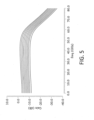
- FIG. 5 is a plot of multiple gain curves across full bandwidth for certain settings of the distributed programmable gain amplifier according to some embodiments of the subject technology. This diagram is merely an example, which should not unduly limit the scope of the claims. One of ordinary skill in the art would recognize many variations, alternatives, and modifications.
- FIG. 5 shows a plot of multiple gain curves across full bandwidth based on certain optimized settings of the distributed programmable gain amplifier shown in FIG. 2 .
- a first characteristic impedance Z 01 is matched to the source resistance Rs.
- a second characteristic impedance Z 02 is matched to the termination resistance Rt.
- the gain as shown in FIG. 5 , is shown to be approximately independent from the frequency. Approximate uniform gain control is achieved with a gain variation just smaller than 2dB across the full bandwidth of 55 GHz or higher. This demonstrates that the distributed gain amplifier has a large bandwidth to meet the demands in modern high-speed communication systems.
- the gain is programmable and can be varied in a large range of at least greater than 11 dB, as shown in FIG. 5 .
- the lower end of the gain range can be expanded somewhat indefinitely, but the higher end of the gain range is limited by parasitic resistance in the signal path.
- FIG. 6 is a plot of multiple input return loss curves over full bandwidth for the same settings of the distributed programmable gain amplifier according to some embodiments of the subject technology. This diagram is merely an example, which should not unduly limit the scope of the claims. One of ordinary skill in the art would recognize many variations, alternatives, and modifications.
- FIG. 6 shows a plot of multiple input return loss curves over the full bandwidth for the same settings as those in FIG. 5 for the distributed programmable gain amplifier shown in FIG. 2 .
- a first characteristic impedance Z 01 is matched to the source resistance Rs.
- the input impedance of the first transmission line is equal to the first characteristic impedance Z 01 due to a matched termination at the second terminal, giving an excellent condition for inducing a minimum return loss for the signal traversing the first transmission line.
- the return loss is smaller than -10 dB for the full bandwidth (55 GHz or higher in this example). Higher frequency also can be achieved within the same scope of the subject technology. This allows the input signal can be coupled to the gain stage with maximum power transfer.
- the distributed input network used in the example shown in FIG. 2 can be extended to have arbitrary number of inductor-capacitor-(or resistor) segments.
- the transmission line by the design of FIG. 2 can be implemented in single-ended as well as in differential circuits.
- the components that are used for building the artificial transmission line may be implemented in many forms and processes. For example, they can be provided as discrete devices (capacitor, inductor, or resistor) on a printed circuit board (PCB). Alternatively, they can also be provided as integrated devices in CMOS processes.
- the resistor network associated with the second circuit and the third circuit can be implemented in different processes including sliding rheostat in discrete implementation, switched resistor array in CMOS processes, and voltage-controlled resistors.
- the wideband gain programmability of the distributed gain amplifier enables SerDes to cope with a large range of operation environments such as >200 Gb/s SerDes transceivers and high-speed switch applications.
Landscapes
- Engineering & Computer Science (AREA)
- Power Engineering (AREA)
- Computer Networks & Wireless Communication (AREA)
- Signal Processing (AREA)
- Microelectronics & Electronic Packaging (AREA)
- Microwave Amplifiers (AREA)
Applications Claiming Priority (1)
| Application Number | Priority Date | Filing Date | Title |
|---|---|---|---|
| US18/498,008 US20250141418A1 (en) | 2023-10-30 | 2023-10-30 | Distributed programmable gain amplifier |
Publications (1)
| Publication Number | Publication Date |
|---|---|
| EP4550663A1 true EP4550663A1 (de) | 2025-05-07 |
Family
ID=92973249
Family Applications (1)
| Application Number | Title | Priority Date | Filing Date |
|---|---|---|---|
| EP24204136.6A Pending EP4550663A1 (de) | 2023-10-30 | 2024-10-02 | Verteilter programmierbarer verstärker |
Country Status (3)
| Country | Link |
|---|---|
| US (1) | US20250141418A1 (de) |
| EP (1) | EP4550663A1 (de) |
| CN (1) | CN119921694A (de) |
Citations (3)
| Publication number | Priority date | Publication date | Assignee | Title |
|---|---|---|---|---|
| US10862521B1 (en) * | 2019-01-30 | 2020-12-08 | Inphi Corporation | Techniques for programmable gain attenuation in wideband matching networks with enhanced bandwidth |
| US20210297293A1 (en) * | 2020-03-18 | 2021-09-23 | Qualcomm Incorporated | Termination for high-frequency transmission lines |
| US20230327623A1 (en) * | 2022-04-08 | 2023-10-12 | Avago Technologies International Sales Pte. Limited | Systems for and methods of wideband distributed amplification |
Family Cites Families (3)
| Publication number | Priority date | Publication date | Assignee | Title |
|---|---|---|---|---|
| JP2002033627A (ja) * | 2000-07-19 | 2002-01-31 | Fujitsu Ltd | 分布増幅器 |
| US6433640B1 (en) * | 2001-05-25 | 2002-08-13 | Motorola, Inc. | Methods and apparatus for amplifying a telecommunication signal |
| US8698570B2 (en) * | 2010-06-07 | 2014-04-15 | Cornell University | Resonator circuit and amplifier circuit |
-
2023
- 2023-10-30 US US18/498,008 patent/US20250141418A1/en active Pending
-
2024
- 2024-08-19 CN CN202411132721.8A patent/CN119921694A/zh active Pending
- 2024-10-02 EP EP24204136.6A patent/EP4550663A1/de active Pending
Patent Citations (3)
| Publication number | Priority date | Publication date | Assignee | Title |
|---|---|---|---|---|
| US10862521B1 (en) * | 2019-01-30 | 2020-12-08 | Inphi Corporation | Techniques for programmable gain attenuation in wideband matching networks with enhanced bandwidth |
| US20210297293A1 (en) * | 2020-03-18 | 2021-09-23 | Qualcomm Incorporated | Termination for high-frequency transmission lines |
| US20230327623A1 (en) * | 2022-04-08 | 2023-10-12 | Avago Technologies International Sales Pte. Limited | Systems for and methods of wideband distributed amplification |
Also Published As
| Publication number | Publication date |
|---|---|
| CN119921694A (zh) | 2025-05-02 |
| US20250141418A1 (en) | 2025-05-01 |
Similar Documents
| Publication | Publication Date | Title |
|---|---|---|
| US10862521B1 (en) | Techniques for programmable gain attenuation in wideband matching networks with enhanced bandwidth | |
| US6768380B2 (en) | Wideband, variable-bandwidth distributed amplifier | |
| US20060202755A1 (en) | Gigabit ethernet transceiver with analog front end | |
| KR20040075351A (ko) | 감쇠기 및 스위치 회로용 회로 토폴로지 | |
| US9154084B2 (en) | Low-noise receiver with complex RF attenuator | |
| US10764092B2 (en) | Input termination circuits for high speed receivers | |
| CN109560830B (zh) | 一种中心频率和群时延均可调的自匹配负群时延电路 | |
| US7804362B2 (en) | Distributed amplifier with negative feedback | |
| US11641181B2 (en) | Compact high gain amplifier with DC coupled stages | |
| US20050168261A1 (en) | High linearity large bandwidth, switch insensitive, programmable gain attenuator | |
| CN112350671B (zh) | 提供可调节信号延迟持续时间的电子电路和方法 | |
| CN216490463U (zh) | 终端电路以及接收器 | |
| AU2008201195A1 (en) | Power divider/combiner and power dividing/combining method using the same | |
| US20250141418A1 (en) | Distributed programmable gain amplifier | |
| CN114650032B (zh) | 用于高速数字接收器的阻抗匹配系统 | |
| CN109449556B (zh) | 混合微带线/共面波导双陷波谐振器、陷波器及电子设备 | |
| US6801098B2 (en) | Group delay equalizer integrated with a wideband distributed amplifier monolithic microwave integrated circuit | |
| KR100653186B1 (ko) | 고주파 가변 감쇠기 | |
| US7352259B2 (en) | Broadband step attenuator with improved time domain performance | |
| KR100972756B1 (ko) | 광대역 감쇠기 | |
| KR102840507B1 (ko) | 트랜지스터 어레이 구조를 사용한 전력소모가 없는 가변 감쇠기 | |
| US6400236B1 (en) | Method and apparatus for a radio frequency power divider having un-terminated outputs | |
| CN110545080A (zh) | 一种基于微带的微波宽带功率均衡器 | |
| US20250062737A1 (en) | Systems and methods for frequency equalization and temperature compensation in radio frequency devices | |
| EP4109752A1 (de) | Breitbandiger signaldämpfer |
Legal Events
| Date | Code | Title | Description |
|---|---|---|---|
| PUAI | Public reference made under article 153(3) epc to a published international application that has entered the european phase |
Free format text: ORIGINAL CODE: 0009012 |
|
| STAA | Information on the status of an ep patent application or granted ep patent |
Free format text: STATUS: THE APPLICATION HAS BEEN PUBLISHED |
|
| AK | Designated contracting states |
Kind code of ref document: A1 Designated state(s): AL AT BE BG CH CY CZ DE DK EE ES FI FR GB GR HR HU IE IS IT LI LT LU LV MC ME MK MT NL NO PL PT RO RS SE SI SK SM TR |
|
| STAA | Information on the status of an ep patent application or granted ep patent |
Free format text: STATUS: REQUEST FOR EXAMINATION WAS MADE |
|
| 17P | Request for examination filed |
Effective date: 20251107 |