EP4553868A2 - Externe elektroden für mehrschichtige elektronische keramische bauelemente mit einer unteren und einer mittleren elektrode auf kupferbasis und einer oberen elektrode auf silberbasis - Google Patents
Externe elektroden für mehrschichtige elektronische keramische bauelemente mit einer unteren und einer mittleren elektrode auf kupferbasis und einer oberen elektrode auf silberbasis Download PDFInfo
- Publication number
- EP4553868A2 EP4553868A2 EP24196674.6A EP24196674A EP4553868A2 EP 4553868 A2 EP4553868 A2 EP 4553868A2 EP 24196674 A EP24196674 A EP 24196674A EP 4553868 A2 EP4553868 A2 EP 4553868A2
- Authority
- EP
- European Patent Office
- Prior art keywords
- electrode layer
- external
- layer
- external electrode
- disposed
- Prior art date
- Legal status (The legal status is an assumption and is not a legal conclusion. Google has not performed a legal analysis and makes no representation as to the accuracy of the status listed.)
- Pending
Links
Images



Classifications
-
- H—ELECTRICITY
- H01—ELECTRIC ELEMENTS
- H01G—CAPACITORS; CAPACITORS, RECTIFIERS, DETECTORS, SWITCHING DEVICES, LIGHT-SENSITIVE OR TEMPERATURE-SENSITIVE DEVICES OF THE ELECTROLYTIC TYPE
- H01G4/00—Fixed capacitors; Processes of their manufacture
- H01G4/002—Details
- H01G4/228—Terminals
- H01G4/232—Terminals electrically connecting two or more layers of a stacked or rolled capacitor
- H01G4/2325—Terminals electrically connecting two or more layers of a stacked or rolled capacitor characterised by the material of the terminals
-
- H—ELECTRICITY
- H01—ELECTRIC ELEMENTS
- H01G—CAPACITORS; CAPACITORS, RECTIFIERS, DETECTORS, SWITCHING DEVICES, LIGHT-SENSITIVE OR TEMPERATURE-SENSITIVE DEVICES OF THE ELECTROLYTIC TYPE
- H01G4/00—Fixed capacitors; Processes of their manufacture
- H01G4/002—Details
- H01G4/018—Dielectrics
- H01G4/06—Solid dielectrics
- H01G4/08—Inorganic dielectrics
- H01G4/12—Ceramic dielectrics
- H01G4/1209—Ceramic dielectrics characterised by the ceramic dielectric material
- H01G4/1218—Ceramic dielectrics characterised by the ceramic dielectric material based on titanium oxides or titanates
- H01G4/1227—Ceramic dielectrics characterised by the ceramic dielectric material based on titanium oxides or titanates based on alkaline earth titanates
-
- H—ELECTRICITY
- H01—ELECTRIC ELEMENTS
- H01G—CAPACITORS; CAPACITORS, RECTIFIERS, DETECTORS, SWITCHING DEVICES, LIGHT-SENSITIVE OR TEMPERATURE-SENSITIVE DEVICES OF THE ELECTROLYTIC TYPE
- H01G4/00—Fixed capacitors; Processes of their manufacture
- H01G4/30—Stacked capacitors
-
- H—ELECTRICITY
- H01—ELECTRIC ELEMENTS
- H01G—CAPACITORS; CAPACITORS, RECTIFIERS, DETECTORS, SWITCHING DEVICES, LIGHT-SENSITIVE OR TEMPERATURE-SENSITIVE DEVICES OF THE ELECTROLYTIC TYPE
- H01G4/00—Fixed capacitors; Processes of their manufacture
- H01G4/002—Details
- H01G4/005—Electrodes
- H01G4/012—Form of non-self-supporting electrodes
-
- H—ELECTRICITY
- H01—ELECTRIC ELEMENTS
- H01G—CAPACITORS; CAPACITORS, RECTIFIERS, DETECTORS, SWITCHING DEVICES, LIGHT-SENSITIVE OR TEMPERATURE-SENSITIVE DEVICES OF THE ELECTROLYTIC TYPE
- H01G4/00—Fixed capacitors; Processes of their manufacture
- H01G4/002—Details
- H01G4/018—Dielectrics
- H01G4/06—Solid dielectrics
- H01G4/08—Inorganic dielectrics
- H01G4/12—Ceramic dielectrics
-
- H—ELECTRICITY
- H01—ELECTRIC ELEMENTS
- H01G—CAPACITORS; CAPACITORS, RECTIFIERS, DETECTORS, SWITCHING DEVICES, LIGHT-SENSITIVE OR TEMPERATURE-SENSITIVE DEVICES OF THE ELECTROLYTIC TYPE
- H01G4/00—Fixed capacitors; Processes of their manufacture
- H01G4/002—Details
- H01G4/228—Terminals
- H01G4/232—Terminals electrically connecting two or more layers of a stacked or rolled capacitor
-
- Y—GENERAL TAGGING OF NEW TECHNOLOGICAL DEVELOPMENTS; GENERAL TAGGING OF CROSS-SECTIONAL TECHNOLOGIES SPANNING OVER SEVERAL SECTIONS OF THE IPC; TECHNICAL SUBJECTS COVERED BY FORMER USPC CROSS-REFERENCE ART COLLECTIONS [XRACs] AND DIGESTS
- Y02—TECHNOLOGIES OR APPLICATIONS FOR MITIGATION OR ADAPTATION AGAINST CLIMATE CHANGE
- Y02E—REDUCTION OF GREENHOUSE GAS [GHG] EMISSIONS, RELATED TO ENERGY GENERATION, TRANSMISSION OR DISTRIBUTION
- Y02E60/00—Enabling technologies; Technologies with a potential or indirect contribution to GHG emissions mitigation
- Y02E60/13—Energy storage using capacitors
Definitions
- the present disclosure relates to a multilayer electronic component.
- a multilayer ceramic capacitor one of multilayer electronic components, may be a chip-type condenser which is mounted on a printed circuit board of any of various electronic products, such as an imaging device such as a liquid crystal display (LCD) or a plasma display panel (PDP), a computer, a smartphone, or a mobile phone, to serve to charge or discharge electricity therein or therefrom.
- an imaging device such as a liquid crystal display (LCD) or a plasma display panel (PDP), a computer, a smartphone, or a mobile phone, to serve to charge or discharge electricity therein or therefrom.
- the MLCC may be used as a component of any of various electronic apparatuses because the MLCC is small, has high capacity, and is easily mounted.
- the external electrode is being thinned to miniaturize the MLCC.
- the external electrode may be formed by a dipping method.
- the external electrode formed by the dipping method may not have a constant thickness, and the external moisture or plating solution may penetrate into the body through a thin portion of the body.
- An aspect of the present disclosure is to provide a multilayer electronic component having improved moisture resistance reliability.
- a multilayer electronic component includes: a body including a dielectric layer and internal electrodes alternately disposed while having the dielectric layer interposed therebetween; and external electrodes disposed on the body, wherein the external electrodes include a lower electrode layer including copper (Cu) and glass, an intermediate electrode layer including copper (Cu) and disposed on the lower electrode layer, and an upper electrode layer including silver (Ag) and glass and disposed on the intermediate electrode layer, and the intermediate electrode layer is a plating layer or a sputtering layer.
- the external electrodes include a lower electrode layer including copper (Cu) and glass, an intermediate electrode layer including copper (Cu) and disposed on the lower electrode layer, and an upper electrode layer including silver (Ag) and glass and disposed on the intermediate electrode layer, and the intermediate electrode layer is a plating layer or a sputtering layer.
- a first direction may indicate a thickness (T) direction
- a second direction may indicate a length (L) direction
- a third direction may indicate a width (W) direction.
- FIG. 1 is a perspective view schematically illustrating a multilayer electronic component according to an exemplary embodiment of the present disclosure.
- FIG. 2 is an exploded perspective view schematically illustrating a body of FIG. 1 .
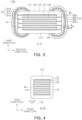
- FIG. 3 is a cross-sectional view schematically illustrating section I-I' in FIG. 1 .
- the body 110 may have first and second surfaces 1 and 2 opposing each other in the first direction, third and fourth surfaces 3 and 4 connected to the first and second surfaces 1 and 2 and opposing each other in the second direction, and fifth and sixth surfaces 5 and 6 connected to the first to fourth surfaces 1, 2, 3 and 4, and opposing each other in the third direction.
- the cover portions 112 and 113 may be formed by stacking a predetermined number of ceramic green sheets on each of which an internal electrode pattern is not printed on both the surfaces of the capacitance formation portion Ac that oppose each other in the first direction, and then sintering the same.
- the average thickness tc of the cover portions 112 or 113 may indicate an average size of the cover portions 112 or 113 in the first direction, and may be an average value of their sizes in the first direction that are measured at five points equally spaced in the second direction in the cross section of the body 110 in the first direction and the second direction, passing through a center of the body 110 in the third direction.
- the external electrodes 131 and 132 may respectively be disposed on the third and fourth surfaces 3 and 4 of the body 110, and extend to some of the first, second, fifth and sixth surfaces 1, 2, 5, and 6.
- the external electrodes 131 and 132 may include the first external electrode 131 connected to the first internal electrode 121 and the second external electrode 132 connected to the second internal electrode 122.
- the external electrode 131 or 132 may include a lower electrode layer 131a or 132a in contact with the internal electrode 121 or 122, an intermediate electrode layer 131b or 132b disposed on the lower electrode layer 131a or 132a, and an upper electrode layer 131c or 132c disposed on the intermediate electrode layer 131b or 132b.
- the first external electrode 131 may include the first lower electrode layer 131a disposed on the third surface 3 and extending to portions of the first and second surfaces 1 and 2, the first intermediate electrode layer 131b covering the first lower electrode layer 131a, and the first upper electrode layer 131c covering the first intermediate electrode layer 131b.
- Each of the lower electrode layer 131a or 132a, the intermediate electrode layer 131b or 132b, and the upper electrode layer 131c or 132c may also partially extend to the fifth and sixth surfaces 5 and 6.
- the lower electrode layer 131a or 132a may include copper (Cu) and glass.
- the lower electrode layer 131a or 132a may include copper (Cu) as its main component.
- a ratio of an area occupied by copper (Cu) to a total area of the lower electrode layer 131a or 132a may be 80% or more when analyzing a cross section of the multilayer electronic component 100 in the first direction and the second direction, passing through the center of the multilayer electronic component 100 in the third direction, by using the scanning electron microscopy (SEM) and energy dispersive spectroscopy (EDS).
- SEM scanning electron microscopy
- EDS energy dispersive spectroscopy
- the ratio of the area occupied by copper (Cu) to the total area of the lower electrode layer 131a or 132a may be greater than a ratio of an area occupied by an element other than copper (Cu) to the total area of the lower electrode layer 131a or 132a, in the cross section of the multilayer electronic component 100 in the first direction and the second direction, passing through the center of the multilayer electronic component 100 in the third direction.
- the total area of the lower electrode layer 131a or 132a may indicate the total area occupied by the lower electrode layer 131a or 132a in an image analyzed by the SEM-EDS.
- the image may be an image illustrating the entire lower electrode layer 131a or 132a, or may be an enlarged image of a portion of the lower electrode layer 131a or 132a.
- the lower electrode layer 131a or 132a may basically serve to electrically connect the internal electrode 121 or 122 to the external electrode 131 or 132.
- the lower electrode layer 131a or 132a may be formed by dipping the third or fourth surface 3 or 4 of the body 110 into a conductive paste for a lower electrode layer that includes a copper (Cu) powder, glass, the binder, the organic solvent, or the like, and then sintering the conductive paste for a lower electrode layer.
- Cu copper
- the intermediate electrode layer 131b or 132b may include copper (Cu).
- the intermediate electrode layer 131b or 132b may include copper (Cu) as its main component.
- a content (at%) of Cu in a total content (at%) of elements included in the intermediate electrode layer 131b or 132b may be 99 at% or more.
- the content (at%) of Cu with respect to the total content (at%) of elements included in the intermediate electrode layer 131b or 132b may be determined by the scanning electron microscopy (SEM) and energy dispersive spectroscopy (EDS).
- a ratio of an area occupied by copper (Cu) to a total area of the intermediate electrode layer 131b or 132b may be 99% or more when analyzing the cross section of the multilayer electronic component 100 in the first direction and the second direction, passing through the center of the multilayer electronic component 100 in the third direction, by using the scanning electron microscopy (SEM) and energy dispersive spectroscopy (EDS) .
- SEM scanning electron microscopy
- EDS energy dispersive spectroscopy
- the total area of the intermediate electrode layer 131b or 132b may indicate the total area occupied by the intermediate electrode layer 131b or 132b in the image analyzed by the SEM-EDS.
- the image may be an image illustrating the entire intermediate electrode layer 131b or 132b, or may be an enlarged image of a portion of the intermediate electrode layer 131b or 132b.
- the intermediate electrode layer 131b or 132b may be formed using an electrolytic plating method, an electroless plating method, an atomic layer deposition (ALD) method, a chemical vapor deposition (CVD) method, and/or a sputtering method.
- the intermediate electrode layer 131b or 132b may be a plating layer.
- the intermediate electrode layer 131b or 132b may be a sputtering layer.
- the intermediate electrode layer 131b or 132b may be formed using the plating method or the sputtering method, and thus be denser than the lower electrode layer 131a or 132a.
- an outer surface of the intermediate electrode layer 131b or 132b may be smoother than that of the lower electrode layer 131a or 132a.
- the upper electrode layer 131c or 132c may include silver (Ag) and glass.
- the upper electrode layer 131c or 132c may include silver (Ag) as its main component.
- a ratio of an area occupied by silver (Ag) to a total area of the upper electrode layer 131c or 132c may be 80% or more when analyzing the cross section of the multilayer electronic component 100 in the first direction and the second direction, passing through the center of the multilayer electronic component 100 in the third direction, by using the scanning electron microscopy (SEM) and energy dispersive spectroscopy (EDS).
- SEM scanning electron microscopy
- EDS energy dispersive spectroscopy
- the ratio of the area occupied by silver (Ag) to the total area of the upper electrode layer 131c or 132c may be greater than a ratio of an area occupied by an element other than silver (Ag) to the total area of the upper electrode layer 131c or 132c, in the cross section of the multilayer electronic component 100 in the first direction and the second direction, passing through the center of the multilayer electronic component 100 in the third direction.
- the total area of the upper electrode layer 131c or 132c may indicate the total area occupied by the upper electrode layer 131c or 132c in the image analyzed by the SEM-EDS.
- the image may be an image illustrating the entire upper electrode layer 131c or 132c, or may be an enlarged image of a portion of the upper electrode layer 131c or 132c.
- a method of forming the upper electrode layer 131c or 132c may not need to be particularly limited.
- the upper electrode layer 131c or 132c may be formed by dipping the body 110, on which the intermediate electrode layer 131b or 132b is formed, into a conductive paste for an upper electrode layer including a silver (Ag) powder, glass, the binder, the organic solvent, or the like, and then sintering the same.
- the external electrode 131 or 132 may include an alloy layer 131d or 132d including a copper (Cu)-silver (Ag) alloy and disposed between the intermediate electrode layer 131b or 132b and the upper electrode layer 131c or 132c. That is, the first external electrode 131 may include the first alloy layer 131d disposed between the first intermediate electrode layer 131b and the first upper electrode layer 131c, and the second external electrode 132 may include the second alloy layer 132d disposed between the second intermediate electrode layer 132b and the second upper electrode layer 132c.
- the alloy layer 131d or 132d may be formed by a mutual reaction between copper (Cu) in the intermediate electrode layer 131b or 132b and silver (Ag) in the upper electrode layer 131c or 132c when the upper electrode layer 131c or 132c is formed by sintering the conductive paste.
- the Cu-Ag alloy included in the alloy layer 131d or 132d may include oxygen (O).
- the alloy layer 131d or 132d may have a higher density than the lower electrode layer 131a or 132a or the upper electrode layer 131c or 132c, thus effectively preventing external moisture or plating solution from penetrating into the body 110.
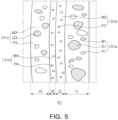
- FIG. 5 shows an enlarged portion of the first external electrode 131.
- the first external electrode 131 and the second external electrode 132 have substantially the same configuration except that the first external electrode 131 is connected to the first the internal electrode 121 and the second external electrode 132 is connected to the second the internal electrode 122. Therefore, the description of FIG. 5 below is considered to include descriptions of both the first and second external electrodes.
- a first metal M1 included in the lower electrode layer 131a may include copper (Cu) as its main component, and may not include silver (Ag). Meanwhile, copper (Cu) may be detected in the first metal M1, and silver (Ag) may not be detected therein when performing the analysis thereon by using the energy dispersive spectroscopy (EDS).
- a glass G1 included in the lower electrode layer 131a or 132a may include one or more oxides of barium (Ba), calcium (Ca), zinc (Zn), aluminum (Al), boron (B), and silicon (Si), and is not limited thereto.
- a second metal M2 included in the intermediate electrode layer 131b may be substantially made of copper (Cu), and may not include silver (Ag). That is, copper (Cu) may be detected in the second metal M2, and silver (Ag) may not be detected therein when performing the analysis thereon by using the energy dispersive spectroscopy (EDS).
- the intermediate electrode layer 131b may include no glass.
- a third metal M3 included in the upper electrode layer 131c may include silver (Ag) as its main component, and may not include copper (Cu). That is, silver (Ag) may be detected in the third metal M3, and copper (Cu) may not be detected therein when performing the analysis thereon by using the energy dispersive spectroscopy (EDS).
- Glass G3 included in the upper electrode layer 131c may include one or more oxides of barium (Ba), calcium (Ca), zinc (Zn), aluminum (Al), boron (B), and silicon (Si), and is not limited thereto.
- a fourth metal M4 included in the alloy layer 131d may be the Cu-Ag alloy. That is, copper (Cu) and silver (Ag) may be detected together in the fourth metal M4 when performing the analysis thereon by using the energy dispersive spectroscopy (EDS).
- EDS energy dispersive spectroscopy
- an area fraction occupied by a pore P2 of the intermediate electrode layer 131b may be smaller than an area fraction occupied by a pore P1 of the lower electrode layer 131a.
- the lower electrode layer 131a may include the plurality of pores P1 therein when formed by sintering the conductive paste.
- the pore may be a path through which the external moisture penetrates into the body 110. Therefore, the external moisture may easily penetrate into the body 110 through the pore P1 of the lower electrode layer 131a, thereby lowering the reliability of multilayer electronic component when the external electrode 131 does not include the intermediate electrode layer 131b.
- an area fraction occupied by a pore P4 of the alloy layer 131d may be smaller than an area fraction occupied by a pore in the upper electrode layer 131c.
- the upper electrode layer 131c may include a number of pores P3 therein when the upper electrode layer 131c is formed by sintering the conductive paste.
- the Cu-Ag alloy layer may be formed by a reaction between the copper (Cu) in the lower electrode layer 131a and silver (Ag) in the upper electrode layer 131c when the external electrode 131 does not include the intermediate electrode layer 131b.
- the Cu-Ag alloy layer may be formed by the reaction between the lower electrode layer 131a and the upper electrode layer 131c, each including a number of pores, to thus have a discontinuous form while having a number of pores formed therein. In this case, it is impossible to effectively suppress the external moisture penetration.
- the alloy layer 131d may be formed by a reaction between the upper electrode layer 131c and the intermediate electrode layer 131b, which has the higher density than the lower electrode layer 131a, to thus have the higher density than the upper electrode layer 131c.
- an average size of the pores P4 included in the alloy layer 131d may be smaller than an average size of the pores P3 included in the upper electrode layer 131c.
- the alloy layer 131d may be formed between the upper electrode layer 131c and the intermediate electrode layer 131b, which has a smooth outer surface and the higher density than the lower electrode layer 131a to thus have continuous form and be disposed at an interface between the intermediate electrode layer 131b and the upper electrode layer 131c. That is, the dense and continuous alloy layer 131d may be formed by the intermediate electrode layer 131b, and the alloy layer 131d may effectively suppress the external moisture penetration.
- a ratio of a length of a region where the alloy layer 131d is disposed to a total length of the interface between the intermediate electrode layer 131b and the upper electrode layer 131c may be 99% or more, in the cross section of the body 110 in the first direction and the second direction, passing through the center of the body 110 in the third direction.
- the lengths and ratio may be measured using a scanning electron microscope (SEM) and an image analysis program. Other methods and/or tools appreciated by one of ordinary skill in the art, even if not described in the present disclosure, may also be used.
- the description describes an example of a method for measuring the area fractions of the pores P1, P2, P3, and P4 respectively included in the lower electrode layer 131a, the intermediate electrode layer 131b, the upper electrode layer 131c, and the alloy layer 131d.
- an enlarged image of an external electrode region in the cross section of the body 110 in the first direction and the second direction, passing through the center of the body 110 in the third direction may be acquired using the scanning electron microscope (SEM).
- SEM scanning electron microscope
- the external electrode region may indicate a central region of the external electrode in the first direction.
- the image may be analyzed using an image analysis program, such as ImageJ program.
- the pores P1, P2, P3, and P4 may be displayed in black, and an area of the pore included in each electrode layer may thus be measured using the image program. Accordingly, it is possible to measure a ratio of an area of the pore P1 to a total area of the lower electrode layer 131a, a ratio of an area of the pore P2 to a total area of the intermediate electrode layer 131b, a ratio of an area of the pore P3 to a total area of the upper electrode layer 131c, and a ratio of an area of the pore P4 to a total area of the alloy layer 131d.
- the average sizes of the pores in the upper electrode layer 131c and in the alloy layer 131d may be measured using a scanning electron microscope (SEM) and an image analysis program. Other methods and/or tools appreciated by one of ordinary skill in the art, even if not described in the present disclosure, may also be used.
- SEM scanning electron microscope
- t1>t3>t2 where t1 indicates a thickness of a central region of the lower electrode layer 131a in the first direction, t2 indicates a thickness of a central region of the intermediate electrode layer 131b in the first direction, and t3 indicates a thickness of a central region of the upper electrode layer 131c in the first direction, in the cross section of the body 110 in the first direction and the second direction, passing through the center of the body 110 in the third direction.
- t1>t3>t2>t4 where t4 indicates a thickness of a central region of the alloy layer 131d in the first direction, in the cross section of the body 110 in the first direction and the second direction, passing through the center of the body 110 in the third direction.
- t1 to t4 may not need to be particularly limited. t1 may be 5 um to 25 ⁇ m, t2 may be 2 um to 4 ⁇ m, t3 may be 1 um to 2 ⁇ m, and t4 may be less than 1 ⁇ m. t1 to t4 may be measured using a scanning electron microscope (SEM) and an image analysis program. Other methods and/or tools appreciated by one of ordinary skill in the art, even if not described in the present disclosure, may also be used.
- SEM scanning electron microscope
- the external electrode 131 or 132 may further include an external plating layer disposed on the upper electrode layer 131c or 132c.
- a type of the external plating layer is not particularly limited, and may be a plating layer including nickel (Ni), tin (Sn), palladium (Pd), and/or an alloy including the same, and may include a plurality of layers.
- the external plating layer may be, for example, a nickel (Ni) plating layer or a tin (Sn) plating layer, and may have the sequentially-formed Ni plating layer and Sn plating layer.
- the external plating layer may include the plurality of Ni plating layers and/or the plurality of Sn plating layers.
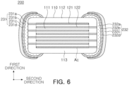
- FIG. 6 is a modified example of the example embodiment illustrated in FIG. 3 , and is a cross-sectional view schematically illustrating a multilayer electronic component 200 according to another exemplary embodiment of the present disclosure.
- the description describes the multilayer electronic component 200 according to another exemplary embodiment of the present disclosure with reference to FIG. 6 , and omits its description overlapping that of the multilayer electronic component 100 according to an exemplary embodiment of the present disclosure described above.
- the first external electrode 231 may include a first lower electrode layer 231a disposed on the third surface 3 and extending to portions of the first and second surfaces 1 and 2, a first intermediate electrode layer 231b covering the first lower electrode layer 231a, and a first upper electrode layer 231c disposed on the first intermediate electrode layer 231b.
- the second external electrode 232 may include a second lower electrode layer 232a disposed on the fourth surface 4 and extending to portions of the first and second surfaces 1 and 2, a second intermediate electrode layer 232b covering the second lower electrode layer 232a, and a second upper electrode layer 232c disposed on the second intermediate electrode layer 232b.
- the first external electrode 231 may include a first alloy layer 231d formed by a reaction between the first intermediate electrode layer 231b and the first upper electrode layer 231c
- the second external electrode 232 may include a second alloy layer 232d formed by a reaction between the second intermediate electrode layer 232b and the second upper electrode layer 232c.
- an end of the first intermediate electrode layer 231b may not be covered by the first upper electrode layer 231c, and an end of the second intermediate electrode layer 232b may not be covered by the second upper electrode layer 232c.
- an end of the intermediate electrode layer 231b or 232b may not be covered by the upper electrode layer 231c or 232c when forming the upper electrode layer 231c or 232c by printing the conductive paste for an upper electrode layer on the intermediate electrode layer 231b or 232b by using the screen printing method and then sintering the same, or attaching the conductive sheet to the intermediate electrode layer 231b or 232b and then sintering the same.
- the alloy layer 231d or 232d may not be formed on the end of the intermediate electrode layer 231b or 232b. In this case, it is possible to improve the moisture resistance reliability of the multilayer electronic component 200 by using the alloy layer 231d or 232d including the Cu-Ag alloy, while achieving the thin external electrode 231 or 232.
- FIG. 7 is a modified example of the example embodiment illustrated in FIG. 3 , and is a cross-sectional view schematically illustrating a multilayer electronic component 300 according to another exemplary embodiment of the present disclosure.
- the description describes the multilayer electronic component 300 according to another exemplary embodiment of the present disclosure with reference to FIG. 7 , and omits its description overlapping that of the multilayer electronic component 100 according to an exemplary embodiment of the present disclosure described above.
- the multilayer electronic component 300 may include the body 110 and first and second external electrodes 331 and 332.
- the first external electrode 331 may include a first lower electrode layer 331a disposed on the third surface 3 and extending to portions of the first and second surfaces 1 and 2, a first intermediate electrode layer 331b covering the first lower electrode layer 331a, and a first upper electrode layer 331c disposed on the first intermediate electrode layer 331b.
- the second external electrode 332 may include a second lower electrode layer 332a disposed on the fourth surface 4 and extending to portions of the first and second surfaces 1 and 2, a second intermediate electrode layer 332b covering the second lower electrode layer 332a, and a second upper electrode layer 332c disposed on the second intermediate electrode layer 332b.
- the first external electrode 331 may include a first alloy layer 331d formed by a reaction between the first intermediate electrode layer 331b and the first upper electrode layer 331c
- the second external electrode 332 may include a second alloy layer 332d formed by a reaction between the second intermediate electrode layer 332b and the second upper electrode layer 332c.
- the first intermediate electrode layer 331b may include a first region R1, which is not covered by the first upper electrode layer 331c, on the third surface 3, and the second intermediate electrode layer 332b may include a second region R2, which is not covered by the second upper electrode layer 332c, on the fourth surface 4.
- the first alloy layer 331d may not be formed on the first region R1, and the second alloy layer 332d may not be formed on the second region R2.
- the moisture resistance reliability of the multilayer electronic component 300 may be improved using the alloy layer 331d or 332d including the Cu-Ag alloy, and an electrical feature of the multilayer electronic component 300 may be improved using the intermediate electrode layer 331b or 332b in direct contact with the external plating layer through the first region R1 and the second region R2.
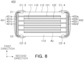
- FIG. 8 is a modified example of the example embodiment illustrated in FIG. 3 , and is a cross-sectional view schematically illustrating a multilayer electronic component 400 according to another exemplary embodiment of the present disclosure.
- the description describes the multilayer electronic component 400 according to another exemplary embodiment of the present disclosure with reference to FIG. 8 , and omits its description overlapping that of the multilayer electronic component 100 according to an exemplary embodiment of the present disclosure described above.
- the multilayer electronic component 400 may include the body 110 and first and second external electrodes 431 and 432.
- the body 110 may have a 1-3-th corner C1-3 connecting the first surface and the third surface to each other, a 1-4-th corner C1-4 connecting the first surface and the fourth surface to each other, a 2-3-th corner C2-3 connecting the second surface and the third surface to each other, and a 2-4-th corner C2-4 connecting the second surface and the fourth surface to each other.
- the body 110 may have a 1-5-th corner connecting the first surface and the fifth surface to each other, a 1-6-th corner connecting the first surface and the sixth surface to each other, a 2-5-th corner connecting the second surface and the fifth surface to each other, and a 2-6-th corner connecting the second surface and the sixth surface to each other.
- the corner may have a round shape by rounding the corner connecting the respective surfaces of the body 110 to each other by performing a separate process.
- the first to sixth surfaces of the body 110 may generally be the flat surfaces, and the non-flat regions may be the corners.
- the first external electrode 431 may include a first lower electrode layer 431a disposed on the third surface 3 and disposed between an extension line E1 of the first surface and an extension line E2 of the second surface, a first intermediate electrode layer 431b covering the first lower electrode layer 431a, and a first upper electrode layer 431c disposed on the first intermediate electrode layer 431b and extending to portions of the first and second surfaces 1 and 2.
- the second external electrode 432 may include a second lower electrode layer 432a disposed on the fourth surface 4 and disposed between the extension line E1 of the first surface and the extension line E2 of the second surface, a second intermediate electrode layer 432b covering the second lower electrode layer 432a, and a second upper electrode layer 432c disposed on the second intermediate electrode layer 432b and extending to portions of the first and second surfaces 1 and 2.
- the upper electrode layer 431c or 432c may partially extend to the fifth and sixth surfaces 5 and 6.
- the first external electrode 431 may include a first alloy layer 431d formed by a reaction between the first intermediate electrode layer 431b and the first upper electrode layer 431c
- the second external electrode 432 may include a second alloy layer 432d formed by a reaction between the second intermediate electrode layer 432b and the second upper electrode layer 432c.
- the moisture resistance reliability of the multilayer electronic component 400 may be improved using the alloy layer 431d or 432d including the Cu-Ag alloy.
- the extension line of each surface may indicate a line extending from a flat portion of each surface.
- the first lower electrode layer 431a may be disposed between the extension line E1 of the first surface and the extension line E2 of the second surface, an end of the first lower electrode layer 431a may thus be disposed on the 1-3-th corner C1-3 and the 2-3-th corner C2-3, and is not limited thereto.
- the second lower electrode layer 432a may be disposed between the extension line E1 of the first surface and the extension line E2 of the second surface, an end of the second lower electrode layer 432a may thus be disposed on the 1-4-th corner C1-4 and the 2-4-th corner C2-4, and is not limited thereto.
- the lower electrode layer 431a or 432a of the multilayer electronic component 400 may be formed by attaching a conductive sheet including the copper (Cu) powder, glass, the binder, or the like to the third or fourth surface 3 or 4 of the body 110 and then firing the same.
- the multilayer electronic component may have the improved moisture resistance reliability.
Landscapes
- Engineering & Computer Science (AREA)
- Power Engineering (AREA)
- Manufacturing & Machinery (AREA)
- Microelectronics & Electronic Packaging (AREA)
- Ceramic Engineering (AREA)
- Chemical & Material Sciences (AREA)
- Inorganic Chemistry (AREA)
- Fixed Capacitors And Capacitor Manufacturing Machines (AREA)
- Ceramic Capacitors (AREA)
- Coils Or Transformers For Communication (AREA)
Applications Claiming Priority (1)
| Application Number | Priority Date | Filing Date | Title |
|---|---|---|---|
| KR1020230154964A KR20250068885A (ko) | 2023-11-10 | 2023-11-10 | 적층형 전자 부품 |
Publications (2)
| Publication Number | Publication Date |
|---|---|
| EP4553868A2 true EP4553868A2 (de) | 2025-05-14 |
| EP4553868A3 EP4553868A3 (de) | 2025-09-03 |
Family
ID=92544257
Family Applications (1)
| Application Number | Title | Priority Date | Filing Date |
|---|---|---|---|
| EP24196674.6A Pending EP4553868A3 (de) | 2023-11-10 | 2024-08-27 | Externe elektroden für mehrschichtige elektronische keramische bauelemente mit einer unteren und einer mittleren elektrode auf kupferbasis und einer oberen elektrode auf silberbasis |
Country Status (5)
| Country | Link |
|---|---|
| US (1) | US20250157738A1 (de) |
| EP (1) | EP4553868A3 (de) |
| JP (1) | JP2025079783A (de) |
| KR (1) | KR20250068885A (de) |
| CN (1) | CN119993741A (de) |
Family Cites Families (4)
| Publication number | Priority date | Publication date | Assignee | Title |
|---|---|---|---|---|
| KR102070235B1 (ko) * | 2018-10-29 | 2020-01-28 | 삼성전기주식회사 | 커패시터 부품 |
| KR102880981B1 (ko) * | 2020-12-14 | 2025-11-04 | 삼성전기주식회사 | 적층형 전자 부품 |
| KR102946062B1 (ko) * | 2021-12-24 | 2026-04-01 | 삼성전기주식회사 | 적층형 전자 부품 |
| KR102881363B1 (ko) * | 2021-12-24 | 2025-11-04 | 삼성전기주식회사 | 적층형 커패시터 |
-
2023
- 2023-11-10 KR KR1020230154964A patent/KR20250068885A/ko active Pending
-
2024
- 2024-08-27 EP EP24196674.6A patent/EP4553868A3/de active Pending
- 2024-09-02 JP JP2024150951A patent/JP2025079783A/ja active Pending
- 2024-09-03 US US18/822,951 patent/US20250157738A1/en active Pending
- 2024-11-08 CN CN202411592520.6A patent/CN119993741A/zh active Pending
Also Published As
| Publication number | Publication date |
|---|---|
| JP2025079783A (ja) | 2025-05-22 |
| CN119993741A (zh) | 2025-05-13 |
| KR20250068885A (ko) | 2025-05-19 |
| US20250157738A1 (en) | 2025-05-15 |
| EP4553868A3 (de) | 2025-09-03 |
Similar Documents
| Publication | Publication Date | Title |
|---|---|---|
| US11361905B2 (en) | Multi-layered ceramic electronic component | |
| CN112309718B (zh) | 多层电子组件 | |
| CN212136266U (zh) | 多层陶瓷电子组件 | |
| EP4553871A2 (de) | Externe elektrode für keramische mehrschichtkapazitoren aufgrund einer grundlegierungsschicht (cu/ag), einer unteren elektrode aufgrund von kupfer (cu) und einer oben elektrode aufgrund von silber (ag) | |
| EP4401104A2 (de) | Mehrschichtiges elektronisches bauteil | |
| US12482606B2 (en) | Multilayered ceramic capacitor | |
| EP4386794A2 (de) | Mehrschichtiges elektronisches bauteil | |
| EP4553868A2 (de) | Externe elektroden für mehrschichtige elektronische keramische bauelemente mit einer unteren und einer mittleren elektrode auf kupferbasis und einer oberen elektrode auf silberbasis | |
| US12278057B2 (en) | Ceramic electronic component including barium calcium titanate | |
| US12278056B2 (en) | Multilayer electronic component | |
| EP4553870A1 (de) | Aussenelektroden für einen mehrschichtigen keramischen kondensator mit einer ersten kupferbasierten elektrode, gefolgt von einer schwach porösen zwischenschicht aus einer silber-kupfer-basierenden legierung mit einer silberbasierten zwischenelektrode | |
| EP4553867A2 (de) | Aussenelektroden für keramische mehrschichtkondensatoren mit einer zwischenschicht aus einer teilweise oxidierten silber- (ag) und (cu) kupferlegierung | |
| EP4535385A1 (de) | Mehrschichtiges elektronisches bauteil | |
| EP4415013B1 (de) | Mehrschichtiges keramisches elektronikbauteil mit einer interdigitalen metallzwischenschicht zwischen der inneren und der äusseren elektrode | |
| EP4415012A1 (de) | Mehrschichtiges elektronisches bauteil | |
| EP4560668A1 (de) | Mehrschichtiges elektronisches bauteil | |
| EP4425514A1 (de) | Mehrschichtiges elektronisches bauteil | |
| EP4604149A1 (de) | Mehrschichtiges elektronisches bauteil | |
| US20240194403A1 (en) | Multilayer electronic component | |
| JP2024085395A (ja) | 積層型電子部品 | |
| KR20250177788A (ko) | 적층형 전자 부품 및 적층형 전자 부품의 제조 방법 | |
| JP2025066637A (ja) | 積層型電子部品 | |
| CN118016447A (zh) | 多层电子组件 |
Legal Events
| Date | Code | Title | Description |
|---|---|---|---|
| PUAI | Public reference made under article 153(3) epc to a published international application that has entered the european phase |
Free format text: ORIGINAL CODE: 0009012 |
|
| STAA | Information on the status of an ep patent application or granted ep patent |
Free format text: STATUS: THE APPLICATION HAS BEEN PUBLISHED |
|
| AK | Designated contracting states |
Kind code of ref document: A2 Designated state(s): AL AT BE BG CH CY CZ DE DK EE ES FI FR GB GR HR HU IE IS IT LI LT LU LV MC ME MK MT NL NO PL PT RO RS SE SI SK SM TR |
|
| PUAL | Search report despatched |
Free format text: ORIGINAL CODE: 0009013 |
|
| AK | Designated contracting states |
Kind code of ref document: A3 Designated state(s): AL AT BE BG CH CY CZ DE DK EE ES FI FR GB GR HR HU IE IS IT LI LT LU LV MC ME MK MT NL NO PL PT RO RS SE SI SK SM TR |
|
| RIC1 | Information provided on ipc code assigned before grant |
Ipc: H01G 4/232 20060101AFI20250731BHEP Ipc: H01G 4/12 20060101ALI20250731BHEP Ipc: H01G 4/30 20060101ALI20250731BHEP Ipc: H01G 4/012 20060101ALI20250731BHEP |
|
| STAA | Information on the status of an ep patent application or granted ep patent |
Free format text: STATUS: REQUEST FOR EXAMINATION WAS MADE |
|
| 17P | Request for examination filed |
Effective date: 20260218 |