EP4554072A1 - Réduction de chevauchement pour convertisseurs de source de courant utilisant des miroirs de courant de grille - Google Patents
Réduction de chevauchement pour convertisseurs de source de courant utilisant des miroirs de courant de grille Download PDFInfo
- Publication number
- EP4554072A1 EP4554072A1 EP23306949.1A EP23306949A EP4554072A1 EP 4554072 A1 EP4554072 A1 EP 4554072A1 EP 23306949 A EP23306949 A EP 23306949A EP 4554072 A1 EP4554072 A1 EP 4554072A1
- Authority
- EP
- European Patent Office
- Prior art keywords
- gate
- switching device
- current
- switching
- devices
- Prior art date
- Legal status (The legal status is an assumption and is not a legal conclusion. Google has not performed a legal analysis and makes no representation as to the accuracy of the status listed.)
- Pending
Links
Images

Classifications
-
- H—ELECTRICITY
- H03—ELECTRONIC CIRCUITRY
- H03K—PULSE TECHNIQUE
- H03K17/00—Electronic switching or gating, i.e. not by contact-making and –breaking
- H03K17/18—Modifications for indicating state of switch
-
- H—ELECTRICITY
- H02—GENERATION; CONVERSION OR DISTRIBUTION OF ELECTRIC POWER
- H02M—APPARATUS FOR CONVERSION BETWEEN AC AND AC, BETWEEN AC AND DC, OR BETWEEN DC AND DC, AND FOR USE WITH MAINS OR SIMILAR POWER SUPPLY SYSTEMS; CONVERSION OF DC OR AC INPUT POWER INTO SURGE OUTPUT POWER; CONTROL OR REGULATION THEREOF
- H02M1/00—Details of apparatus for conversion
- H02M1/08—Circuits specially adapted for the generation of control voltages for semiconductor devices incorporated in static converters
- H02M1/084—Circuits specially adapted for the generation of control voltages for semiconductor devices incorporated in static converters using a control circuit common to several phases of a multi-phase system
-
- H—ELECTRICITY
- H02—GENERATION; CONVERSION OR DISTRIBUTION OF ELECTRIC POWER
- H02M—APPARATUS FOR CONVERSION BETWEEN AC AND AC, BETWEEN AC AND DC, OR BETWEEN DC AND DC, AND FOR USE WITH MAINS OR SIMILAR POWER SUPPLY SYSTEMS; CONVERSION OF DC OR AC INPUT POWER INTO SURGE OUTPUT POWER; CONTROL OR REGULATION THEREOF
- H02M7/00—Conversion of AC power input into DC power output; Conversion of DC power input into AC power output
- H02M7/42—Conversion of DC power input into AC power output without possibility of reversal
- H02M7/44—Conversion of DC power input into AC power output without possibility of reversal by static converters
- H02M7/48—Conversion of DC power input into AC power output without possibility of reversal by static converters using discharge tubes with control electrode or semiconductor devices with control electrode
- H02M7/53—Conversion of DC power input into AC power output without possibility of reversal by static converters using discharge tubes with control electrode or semiconductor devices with control electrode using devices of a triode or transistor type requiring continuous application of a control signal
- H02M7/537—Conversion of DC power input into AC power output without possibility of reversal by static converters using discharge tubes with control electrode or semiconductor devices with control electrode using devices of a triode or transistor type requiring continuous application of a control signal using semiconductor devices only, e.g. single switched pulse inverters
- H02M7/5387—Conversion of DC power input into AC power output without possibility of reversal by static converters using discharge tubes with control electrode or semiconductor devices with control electrode using devices of a triode or transistor type requiring continuous application of a control signal using semiconductor devices only, e.g. single switched pulse inverters in a bridge configuration
- H02M7/53871—Conversion of DC power input into AC power output without possibility of reversal by static converters using discharge tubes with control electrode or semiconductor devices with control electrode using devices of a triode or transistor type requiring continuous application of a control signal using semiconductor devices only, e.g. single switched pulse inverters in a bridge configuration with automatic control of output voltage or current
-
- H—ELECTRICITY
- H03—ELECTRONIC CIRCUITRY
- H03K—PULSE TECHNIQUE
- H03K17/00—Electronic switching or gating, i.e. not by contact-making and –breaking
- H03K17/51—Electronic switching or gating, i.e. not by contact-making and –breaking characterised by the components used
- H03K17/56—Electronic switching or gating, i.e. not by contact-making and –breaking characterised by the components used by the use, as active elements, of semiconductor devices
- H03K17/687—Electronic switching or gating, i.e. not by contact-making and –breaking characterised by the components used by the use, as active elements, of semiconductor devices the devices being field-effect transistors
- H03K17/689—Electronic switching or gating, i.e. not by contact-making and –breaking characterised by the components used by the use, as active elements, of semiconductor devices the devices being field-effect transistors with galvanic isolation between the control circuit and the output circuit
-
- H—ELECTRICITY
- H03—ELECTRONIC CIRCUITRY
- H03K—PULSE TECHNIQUE
- H03K17/00—Electronic switching or gating, i.e. not by contact-making and –breaking
- H03K17/51—Electronic switching or gating, i.e. not by contact-making and –breaking characterised by the components used
- H03K17/56—Electronic switching or gating, i.e. not by contact-making and –breaking characterised by the components used by the use, as active elements, of semiconductor devices
- H03K17/687—Electronic switching or gating, i.e. not by contact-making and –breaking characterised by the components used by the use, as active elements, of semiconductor devices the devices being field-effect transistors
- H03K17/689—Electronic switching or gating, i.e. not by contact-making and –breaking characterised by the components used by the use, as active elements, of semiconductor devices the devices being field-effect transistors with galvanic isolation between the control circuit and the output circuit
- H03K17/691—Electronic switching or gating, i.e. not by contact-making and –breaking characterised by the components used by the use, as active elements, of semiconductor devices the devices being field-effect transistors with galvanic isolation between the control circuit and the output circuit using transformer coupling
-
- H—ELECTRICITY
- H03—ELECTRONIC CIRCUITRY
- H03K—PULSE TECHNIQUE
- H03K17/00—Electronic switching or gating, i.e. not by contact-making and –breaking
- H03K17/51—Electronic switching or gating, i.e. not by contact-making and –breaking characterised by the components used
- H03K17/78—Electronic switching or gating, i.e. not by contact-making and –breaking characterised by the components used using opto-electronic devices, i.e. light-emitting and photoelectric devices electrically- or optically-coupled
Definitions
- This disclosure pertains to the field of current source converters comprising at least two switching half-bridges having each an upper switching device and a lower switching device and where a ON state overlapping between upper switching devices or between lower switching devices of two half-bridges having opposite switching transition periods is needed to avoid a current interruption which would cause an overvoltage in the converter.
- CSC Current source power converters
- CSC Current source power converters
- the switches of the upper legs of two half-bridges and the switches of the lower legs of two half-bridges are controlled in a complementary way with conducting to blocking and blocking to conducting transitions. Between these transitions, overlapping where both upper switches, or both lower switches are ON is used.
- the main reason of the overlapping is due to the nature of the current source which is an inductive source which should not be interrupted. Current interruption can be due to multiple factors, including wrong control signal of one of the two switches, a faulty device failed in open circuit or a failed gate driver.
- a reduction of the overlapping time is beneficial for the overall converter operation.
- a too high overlapping time would lead to a high Total Harmonic Distortion (THD) of the output current.
- TDD Total Harmonic Distortion
- Some software solutions can be implemented in the control loop to mitigate such side effects.
- the reduction of the overlapping time could reduce the losses in case of a CSC having current bidirectionality feature, see the device assembly presented in the circle A of Figure 1 .
- the control of the two devices placed in series depends on the overlapping time, the longer the overlapping time, the longer is the conduction of one of the body diodes, thus the conduction losses increase because of the high forward voltage.
- This disclosure improves the situation in providing a switching system where the overlapping between conducting to non-conducting and non-conducting to conducting power semiconductor switches in a current fed converter is reduced without the need of reducing the overlapping calculated by a controller of the converter.
- the present disclosure proposes a control circuit for a current source converter having a current generator comprising an inductance and having two or more half bridges each half bridge having an upper leg provided with an upper switching device and a lower leg provided with a lower switching device, said upper legs switching devices and said lower legs switching devices being controlled by a controller to provide an overlap between an upper leg turning off switching device and an upper leg turning on switching device and to provide an overlap between a lower leg turning on switching device and a lower leg turning off switching device through gate pull up and gate pull down pulse signals to gate drivers buffers of said switching devices, characterized in that said gate driver circuit comprises:
- Said gate pull-down signal may be output from a MOS transistor which gate receives a pulse issued from said gate current mirroring circuit, said MOS transistor having or not a filtering capacitor between the gate and a source of said MOS transistor.
- Said gate pull-down signal may be an output of a SR gate having as input a current image of the gate current and issued from said gate current mirroring circuit.
- the control circuit may comprise an inverter gate to provide said reset signal from said positive gate command connection path.
- Said reset signal may polarize a gate of a MOS transistor to discharge the gate of said MOS transistor or to discharge the gate of said MOS transistor and said filtering capacitor.
- said reset signal When said gate pull-down signal is an output of a SR gate having as input a current image of the gate current and issued from said gate current mirroring circuit, said reset signal may be connected to a reset input of said SR gate.
- the pre-driver may provide a first galvanic isolation between a controller circuit and the gate buffer.
- the control circuit may comprise a second galvanic isolation between the gate current mirror circuit and the gate pull down signal circuit.
- Said second galvanic isolation may be provided with a transformer in the collector branch of a current mirror transistor.
- Said second galvanic isolation may also be provided with a photocoupler in the collector branch of a current mirror transistor or another insulating component.
- the present disclosure also concerns a converter or an inverter comprising a current source, a controller, at least two half-bridges provided with upper legs switching devices and lower legs switching devices, each of said switching devices being controlled by said controller through gate drivers, wherein said gate drivers comprise control circuits according to any one of the preceding claims.
- the present disclosure concerns further a method for switching power switch devices of legs of half-bridges of a current source converter with reduced overlapping time, where ON, OFF states of said power switch devices of said legs are driven by a controller through gate drivers provided with gate buffers, characterized in that during a switching transition between a first upper leg power switch device and a second upper leg power switch device or a switching transition between a first lower leg power switch device and a second lower leg power switch device, said switching transitions being initiated by a controller through said gate drivers of the power switch devices, the method comprises using a mirrored gate current, or a voltage proportional to such mirrored gate current, from one of said power switch devices having an OFF state to ON state transition in order to commutate the other of said switches devices from a ON state to an OFF state earlier than a gate pulse issued from said controller to a gate driver of said second switch device provided for commutating said other of said switches devices from said ON state to said OFF state.
- the method may comprise providing a gate pull down pulse signal issued from said mirrored gate current, or a voltage proportional to such mirrored gate current, said gate pull down pulse signal being used for commutating the other of said switches devices from said ON state to said OFF state.
- Said mirrored gate current may be a mirrored source current of gate buffers driving said power switch devices.
- the method may comprise latching said mirrored gate current or voltage proportional to said mirrored gate current to provide said gate pull down pulse signal and resetting said gate pull down pulse signal at an end of said transition.
- FIG. 1 is a schematic view of a DC/AC current source converter also called inverter.
- Such converter comprises a DC source 1 an inductance 2 and two half bridges.
- a first half-bridge comprises first upper leg power switch device 11 with IGBT Q1 and a diode 21 and first lower leg power switch device 12 with IGBT Q2 and diode 22.
- a second half-bridge comprises second upper leg power switch device 13 with IGBT Q3 and a diode 23 and second lower leg power switch device 14 with IGBT Q4 and diode 24.
- the IGBT+ diode design shown may be replaced with serial opposite polarity IGBTs with reverse freewheeling diodes or serial reverse polarity MOSFET having inherent body diode or with additional freewheeling diodes such as in circle A.
- the half-bridges of the current source converter are connected to an alternating voltage and current load 4.
- the switches are controlled through gate drivers, a first gate driver 31 for the first half-bridge first upper leg switch device 11, a second gate driver 32 for the first half-bridge first lower switch device 12, a third gate driver 33 for the second upper leg switch device 13 of the second half bridge and gate driver 34 for the second lower leg switch device 14 of the second half-bridge.
- gate drivers a first gate driver 31 for the first half-bridge first upper leg switch device 11, a second gate driver 32 for the first half-bridge first lower switch device 12, a third gate driver 33 for the second upper leg switch device 13 of the second half bridge and gate driver 34 for the second lower leg switch device 14 of the second half-bridge.
- the present disclosure concerns a driver circuit that aims to reduce the overlap in order to reduce losses in the converter and heat dissipation in the power switches.
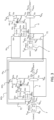
- driver circuit is designed as in figure 2 or in figure 3 to add an early turn OFF function of a first switch upon turning ON of a second switch in the same leg level (upper leg level or lower leg level) in the driver circuit.
- the driver circuit 31 comprises a pre-driver 7 which provides a first galvanic isolation between the controller power supply V DD , Vss and the power switch X gate buffer circuit 6 having a V DDx and V SSx power supply.
- a gate current mirror circuit 51 having transistors T3 and T4 is positioned in the source branch of the push pull buffer 6 having transistors T1 and T2.
- the image of the source current of the buffer 6 is taken at the junction of the resistor R MON and the collector of transistor T5.
- This source current corresponds to the gate current of the power switch device X during its OFF to ON transition.
- a second galvanic isolation 52 made with an optocoupler 52a transfers the signal extracted from the current mirror to a SR gate which output provides a signal Gp y used as discussed hereunder to turn off a power switch device Y, as seen in figure 3 , prior to reception of the controller switch closing signal I-.
- the same driver circuit is realized for the power switch Y and the power device Y provides in turn a Gp x signal which will turn off the power switch device X OFF prior to reception of the controller signal during an OFF to ON transition of the power switch device Y.
- the SR gates are replaced by MOS transistors Q1x, Q2x in the driver circuit of the gate Y of power switch Y and Q1y, Q2y in the driver circuit of the gate X of power switch X.
- These MOS transistors receive an image of the gate driver current through transformers TRx and Try which provide the second galvanic isolation in replacement of the optocouplers 52a.
- the image from the gate driver current of switch Y goes through a Schottky diode D1x and on the gate of Q2x to provide the signal GPx that will pull down the gate buffer of switch X
- the image from the gate driver current of switch X goes through a Schottky diode D1y and on the gate of Q2y to provide the signal GPy that will pull down the gate buffer of switch Y.
- the O+ signal to turn on switch Y provides the signal RSTy through an inverter 71, such signal being provided to pull down the gate of MOS transistor Q2y through MOS transistor Q1y and the O+ signal to turn on switch X provides the signal RSTx through a further inverter 71, such signal being provided to pull down the gate of MOS transistor Q2x through MOS transistor Q1x.
- This second realization mode only based on transistors and passive components is simpler to embed in a power module than logic components as in figure 2 and provides the same function.
- the disclosed circuits provide a simple way to reduce the ON overlap between switches without creating open circuit conditions since it is based on detection of the OFF to ON transition of a first switch to anticipate the ON to OFF transition of the second switch which is controlled in a complementary way from the first switch.
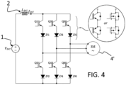
- control circuit described may be adapted to a three-phase output current source converter as per figure 4 with the use of adapted logic circuits and isolation to combine the gate command signals and gate pull down detection signals of three half-bridges.
- present disclosure may be applied to DC/AC converters but also to AC/DC converters, the source and load being reversed.
- the present invention may be combined with a circuit designed to protect the current source converter, such circuit using a sink current mirror circuit similar to the source current mirror depicted.
Landscapes
- Engineering & Computer Science (AREA)
- Power Engineering (AREA)
- Power Conversion In General (AREA)
- Inverter Devices (AREA)
Priority Applications (2)
| Application Number | Priority Date | Filing Date | Title |
|---|---|---|---|
| EP23306949.1A EP4554072A1 (fr) | 2023-11-10 | 2023-11-10 | Réduction de chevauchement pour convertisseurs de source de courant utilisant des miroirs de courant de grille |
| PCT/JP2024/080103 WO2025100554A1 (fr) | 2023-11-10 | 2024-07-02 | Réduction du chevauchement pour convertisseurs de source de courant utilisant des miroirs de courant de grille |
Applications Claiming Priority (1)
| Application Number | Priority Date | Filing Date | Title |
|---|---|---|---|
| EP23306949.1A EP4554072A1 (fr) | 2023-11-10 | 2023-11-10 | Réduction de chevauchement pour convertisseurs de source de courant utilisant des miroirs de courant de grille |
Publications (1)
| Publication Number | Publication Date |
|---|---|
| EP4554072A1 true EP4554072A1 (fr) | 2025-05-14 |
Family
ID=89119458
Family Applications (1)
| Application Number | Title | Priority Date | Filing Date |
|---|---|---|---|
| EP23306949.1A Pending EP4554072A1 (fr) | 2023-11-10 | 2023-11-10 | Réduction de chevauchement pour convertisseurs de source de courant utilisant des miroirs de courant de grille |
Country Status (2)
| Country | Link |
|---|---|
| EP (1) | EP4554072A1 (fr) |
| WO (1) | WO2025100554A1 (fr) |
Citations (1)
| Publication number | Priority date | Publication date | Assignee | Title |
|---|---|---|---|---|
| CN114221567A (zh) * | 2021-12-30 | 2022-03-22 | 东莞市双平电源技术有限公司 | 一种以lcr并联结构作为负载的逆变电路及其工作方法 |
-
2023
- 2023-11-10 EP EP23306949.1A patent/EP4554072A1/fr active Pending
-
2024
- 2024-07-02 WO PCT/JP2024/080103 patent/WO2025100554A1/fr active Pending
Patent Citations (1)
| Publication number | Priority date | Publication date | Assignee | Title |
|---|---|---|---|---|
| CN114221567A (zh) * | 2021-12-30 | 2022-03-22 | 东莞市双平电源技术有限公司 | 一种以lcr并联结构作为负载的逆变电路及其工作方法 |
Non-Patent Citations (1)
| Title |
|---|
| BEN GUO ET AL: "Compensation of input current distortion in three-phase buck rectifiers", APPLIED POWER ELECTRONICS CONFERENCE AND EXPOSITION (APEC), 2013 TWENTY-EIGHTH ANNUAL IEEE, IEEE, 17 March 2013 (2013-03-17), pages 930 - 938, XP032410447, ISBN: 978-1-4673-4354-1, DOI: 10.1109/APEC.2013.6520325 * |
Also Published As
| Publication number | Publication date |
|---|---|
| WO2025100554A1 (fr) | 2025-05-15 |
Similar Documents
| Publication | Publication Date | Title |
|---|---|---|
| US6483724B1 (en) | DC/DC ZVS full bridge converter power supply method and apparatus | |
| CA3006344C (fr) | Topologie a tolerance de pannes pour convertisseurs multiniveaux du type en t | |
| CA2320328C (fr) | Redressement synchrone automatique | |
| US8866342B2 (en) | Power converting apparatus | |
| US20120187879A1 (en) | Zero-voltage-transition soft switching converter | |
| US11387746B2 (en) | Current source inverter with bi-directional switches | |
| US12573956B2 (en) | Converter for power conversion, three-phase converter arrangement and method for packaging a converter | |
| EP2858221A1 (fr) | Protection contre les courts-circuits | |
| EP4554072A1 (fr) | Réduction de chevauchement pour convertisseurs de source de courant utilisant des miroirs de courant de grille | |
| US11750109B2 (en) | Power conversion device | |
| US12375004B2 (en) | Synchronous reverse blocking switch for soft-switching current source converters and soft-switching current source converters including the same | |
| US12255550B2 (en) | Current source inverter using bidirectional switches with bidirectional power flow capability | |
| EP4554092A1 (fr) | Protection contre l'interruption de courant pour convertisseurs de source de courant utilisant des miroirs de courant de grille | |
| CN118631030B (zh) | 用于电机驱动的功率半导体电路 | |
| JP7522292B2 (ja) | 電力変換装置及びその制御方法 | |
| EP3411947A1 (fr) | Modules ups et conditionnement de puissance | |
| CN106655859B (zh) | 一种用于电机驱动电路的桥臂及其控制方法 | |
| KR102573204B1 (ko) | 전력 변환 장치 및 그 제어 방법 | |
| US12101038B2 (en) | Uninterruptible power supply having short circuit load capability | |
| US20260008354A1 (en) | Multi-phase full-bridge drive system and method for driving motor | |
| Nakayama et al. | High-frequency quasi-Z-source inverter concept for short-circuit capable GaN-HEMT-based converters | |
| KR102381873B1 (ko) | 전력 변환 장치 및 그 제어 방법 | |
| McNeill et al. | Fundamental Comparison of Efficiencies of Voltage Source Converter Phase-Leg Configurations with Super-Junction MOSFETs | |
| CN118891813A (zh) | 高功率的dc/dc转换器 | |
| PL207881B1 (pl) | Sposób zabezpieczania łącznika mocy w przekształtniku mocy oraz przekształtnik mocy |
Legal Events
| Date | Code | Title | Description |
|---|---|---|---|
| PUAI | Public reference made under article 153(3) epc to a published international application that has entered the european phase |
Free format text: ORIGINAL CODE: 0009012 |
|
| STAA | Information on the status of an ep patent application or granted ep patent |
Free format text: STATUS: THE APPLICATION HAS BEEN PUBLISHED |
|
| AK | Designated contracting states |
Kind code of ref document: A1 Designated state(s): AL AT BE BG CH CY CZ DE DK EE ES FI FR GB GR HR HU IE IS IT LI LT LU LV MC ME MK MT NL NO PL PT RO RS SE SI SK SM TR |
|
| STAA | Information on the status of an ep patent application or granted ep patent |
Free format text: STATUS: REQUEST FOR EXAMINATION WAS MADE |
|
| 17P | Request for examination filed |
Effective date: 20250814 |
|
| STAA | Information on the status of an ep patent application or granted ep patent |
Free format text: STATUS: EXAMINATION IS IN PROGRESS |
|
| 17Q | First examination report despatched |
Effective date: 20251117 |