EP4556896A1 - Beleuchtungsempfangssystem und messverfahren - Google Patents
Beleuchtungsempfangssystem und messverfahren Download PDFInfo
- Publication number
- EP4556896A1 EP4556896A1 EP24211215.9A EP24211215A EP4556896A1 EP 4556896 A1 EP4556896 A1 EP 4556896A1 EP 24211215 A EP24211215 A EP 24211215A EP 4556896 A1 EP4556896 A1 EP 4556896A1
- Authority
- EP
- European Patent Office
- Prior art keywords
- light
- aperture
- illumination
- receiving cavity
- yarn
- Prior art date
- Legal status (The legal status is an assumption and is not a legal conclusion. Google has not performed a legal analysis and makes no representation as to the accuracy of the status listed.)
- Pending
Links
Images




Classifications
-
- G—PHYSICS
- G01—MEASURING; TESTING
- G01N—INVESTIGATING OR ANALYSING MATERIALS BY DETERMINING THEIR CHEMICAL OR PHYSICAL PROPERTIES
- G01N21/00—Investigating or analysing materials by the use of optical means, i.e. using sub-millimetre waves, infrared, visible or ultraviolet light
- G01N21/84—Systems specially adapted for particular applications
- G01N21/88—Investigating the presence of flaws or contamination
- G01N21/8806—Specially adapted optical and illumination features
-
- G—PHYSICS
- G01—MEASURING; TESTING
- G01N—INVESTIGATING OR ANALYSING MATERIALS BY DETERMINING THEIR CHEMICAL OR PHYSICAL PROPERTIES
- G01N21/00—Investigating or analysing materials by the use of optical means, i.e. using sub-millimetre waves, infrared, visible or ultraviolet light
- G01N21/01—Arrangements or apparatus for facilitating the optical investigation
-
- G—PHYSICS
- G01—MEASURING; TESTING
- G01N—INVESTIGATING OR ANALYSING MATERIALS BY DETERMINING THEIR CHEMICAL OR PHYSICAL PROPERTIES
- G01N21/00—Investigating or analysing materials by the use of optical means, i.e. using sub-millimetre waves, infrared, visible or ultraviolet light
- G01N21/84—Systems specially adapted for particular applications
- G01N21/88—Investigating the presence of flaws or contamination
-
- G—PHYSICS
- G01—MEASURING; TESTING
- G01N—INVESTIGATING OR ANALYSING MATERIALS BY DETERMINING THEIR CHEMICAL OR PHYSICAL PROPERTIES
- G01N21/00—Investigating or analysing materials by the use of optical means, i.e. using sub-millimetre waves, infrared, visible or ultraviolet light
- G01N21/84—Systems specially adapted for particular applications
- G01N21/88—Investigating the presence of flaws or contamination
- G01N21/89—Investigating the presence of flaws or contamination in moving material, e.g. running paper or textiles
- G01N21/8914—Investigating the presence of flaws or contamination in moving material, e.g. running paper or textiles characterised by the material examined
- G01N21/8915—Investigating the presence of flaws or contamination in moving material, e.g. running paper or textiles characterised by the material examined non-woven textile material
-
- B—PERFORMING OPERATIONS; TRANSPORTING
- B65—CONVEYING; PACKING; STORING; HANDLING THIN OR FILAMENTARY MATERIAL
- B65H—HANDLING THIN OR FILAMENTARY MATERIAL, e.g. SHEETS, WEBS, CABLES
- B65H63/00—Warning or safety devices, e.g. automatic fault detectors, stop-motions ; Quality control of the package
- B65H63/06—Warning or safety devices, e.g. automatic fault detectors, stop-motions ; Quality control of the package responsive to presence of irregularities in running material, e.g. for severing the material at irregularities ; Control of the correct working of the yarn cleaner
- B65H63/062—Electronic slub detector
- B65H63/065—Electronic slub detector using photo-electric sensing means, i.e. the defect signal is a variation of light energy
Definitions
- the invention refers to an illumination receiving system.
- the invention refers to a clearer.
- the invention also refers to a textile machine.
- the invention refers to a method of manufacturing.
- the invention refers to a method for measuring.
- a clearer comprises a yarn sensor for optically scanning a yarn moving longitudinally in a measuring gap supplied with light rays from a source with a first receiver for directly transmitted light, two further receivers for light reflected from the yarn and elements for transmitting light between the source, gap and receivers.
- the transmitting element between the source and gap includes a diffusing foil, an aperture, and a lens behind the source in the radiation direction, such that the aperture is imaged at infinity.
- the transmitting elements between the gap and reflected light receivers each contain a lens before the receiver in the radiation direction, such that an image discernable by each receiver lies, in the absence of yarn on the opposite wall of the measurement gap, such that each image of the reflected light receivers lies crosswise on the other side and outside of the image of the source on the wall.
- the clearer in the art provides a complex and difficult to handle optical setup in combination with a complex housing which limits the potential of the clearer with respect to the optical setup capabilities. Furthermore, the clearer in the art is complex in assemblance and therefore tedious to assemble, which binds resources in doing so.
- the object is solved by an illumination receiving system with the features of claim 1. Further, the object is solved by a clearer with the features of claim 11. The object is solved by a textile machine with the features of claim 11. The object is solved by a method of manufacturing an illumination receiving system with the features of claim 12. The object is solved by a method for measuring with the features of claim 17.
- the object is solved by a housing with the features of claim 1.
- an illumination receiving system may be configured for receiving a shadow projection from an object or may be configured for receiving reflected light from an object, particularly in a textile machine.
- the illumination receiving system may comprise at least one receiving cavity.
- the illumination receiving system may comprise at least one photo sensitive electronical component.
- the receiving cavity is particularly configured and placed relative to an object such that light emitted from a light source and projecting a shadow from the object to enter the receiving cavity.
- the receiving cavity is particularly configured and placed relative to an object such that light being reflected from the object to enter the receiving cavity.
- the light entering the receiving cavity is particularly transmitted to the at least one photo sensitive electronical component for measuring the incoming illumination.
- the proposed illumination receiving system may foresee multiple non-specular reflections of the incoming illumination in the measurement cavity.
- the multiple non-specular reflections of the incoming illumination may result in an even illumination of the whole cavity surface.
- the structure or image of the projection can thus be destroyed.
- the measurement can be an integral measurement of all the light captured through the aperture of the receiving system.
- the complete optical setup may not require a separate and individual diffusing sheet e.g., a diffusor.
- the task of measuring the characteristics of the object between an illumination projector and the illumination receiving system may be reduced to measurements of the illumination strength of the cavity surface.
- the opening aperture of the receiving system and the size of the photo sensitive electronical component can be decoupled.
- the cross section of the opening aperture of the illumination receiving system can be varied independently with respect to the size of the photo sensitive electronical component and vice versa.
- the setup is simple to handle and therefore reduces the necessary maintenance, set up and handling resources.
- the object may particularly be at least one of a string-like textile formation, a yarn, a sliver, a rover or a singular item, particularly placed inside a measurement gap of a sensor, particularly in a textile machine.
- a photosensitive electronical component may be any type of photosensitive detector or part thereof interacting with the incoming (the received) light.
- the photosensitive electronical component may be a photodiode e.g., a GaAs material configured to detect light and transforming the incoming light into an electronical signal.
- the light source may be positioned relative to a measurement gap, wherein a yarn can be guided.
- the guiding of a yarn can be implemented such that the yarn passes relative to an illumination spot, an illumination area and/or an illumination volume.
- the yarn may interact with the light emitted from a light source to project a shadow or to reflect light from the yarn to the illumination receiving system.
- the yarn, its parts or components thereof may interact with the light and may cause scattering and/or may absorb light of certain wavelengths. All these interactions may be indicative of yarn characteristics, such as impurities, defects, fiber damages etc.
- the yarn is guided between two points where it interacts with a yarn guiding device as described elsewhere herein.
- a light source is configured to transmit light via optics to a certain illumination spot, illumination area and/or illumination volume as described elsewhere herein.
- the illumination receiving system may function as a receiver and may comprise optics to transfer light from the illumination spot, the illumination area and/or the illumination volume to a photosensitive detector system (also referred to as photosensitive electronic component).
- a photosensitive detector system also referred to as photosensitive electronic component.
- the combination of light source, photosensitive detector (as an embodiment or synonym of a photosensitive electronical component) and the optics in at least one beam path there between may be referred to as an optical setup.
- the light source might be any type of light source emitting light that is capable of performing the respective tasks as described in detail elsewhere herein.
- a light source might be a light emitting diode, or in short, an LED, a laser diode, a continuous wave laser, a pulsed laser, etc.
- a receiving cavity is particularly configured to receive light projecting a shadow from a yarn into the receiving cavity. Therefore, the shadow may indicate differences on sectional parts of the yarn moving by in the measuring gap.
- the yarn is moving by particularly because it is made in a spinning device of a textile machine and thereafter it can be checked for the resulting quality. This might be one exemplary application of the respective illumination receiving system, particularly in a clearer of a textile machine as described elsewhere herein.
- the photosensitive electronical component is mounted in a position such that the photosensitive electronical component is out of line-of-sight of the incoming light projecting a shadow from the object and/or reflecting light from the object into the receiving cavity.
- the photosensitive electrical component has particularly no direct line of sight to the illumination projector as a type of projection system. Without direct line of sight of the photosensitive electrical components, no diffusor may be required.
- the photosensitive electrical component can be placed in plane to the signal processing PCBA.
- the required electronics can be assembled in a cost conserving single part with a single manufacturing pass of method steps.
- a PCBA, short for printed circuit board assembly particularly refers to the combination of a PCB, short for a printed circuit board, and components and electronic accessories.
- the PCBA can be placed such that it comprises at least one of the light source or the photosensitive detector.
- the light source may be a light emitting diode, short LED.
- the photosensitive detector may be a photodiode that can sense light for transforming it into an electronic signal. At least one of the light source or the photosensitive detector may be placed in plane with the PCB.
- the combination of a PCB with at least one of photosensitive detector or light source may render it to a PCBA.
- the PCBA may comprise at least one alignment structure that is configured and positioned to allow for an alignment of the PCBA with respect to other optical components described elsewhere herein to assemble an optical setup by placing the PCB onto the respective optical components, particularly assembling the illumination receiving system.
- optical setup The light source, the photosensitive electrical component (as part of the photosensitive detector) and any optics there between may be referred to as optical setup.
- the photosensitive electronical component can measure the brightness of the entrapped incoming illumination by the receiving cavity (the lighthouse). This can represent an indirect measurement. Due to this indirect measurement, the size of the photosensitive electronical component may not be coupled or may be independent of the size of the object to be measured. This allows for a selection of the most suitable photosensitive electronical component, particular with criteria being one or a combination of response time, sensitivity, wavelength range, sensitivity over wavelength, Noise Equivalent Power, active size, packaging type, cost, etc. This selection criteria can be much wider compared to known solutions in the art and may allow for optimization, where the first criteria to be met may be the maximum defect size that is to be measured.
- an aperture can be placed at the entrance of the receiving cavity. This allows to block out unwanted environmental light.
- a thin aperture may allow light from all angles of the opening hemisphere to go through the aperture opening.
- a thin aperture has no angular blocking.
- a thick aperture on the contrary provides an angular blocking of incoming (received) rays of light (also to be referred to as light beams).
- the aperture may be attached to the receiving cavity, particularly the lighthouse, directly. Such a direct attachment of the receiving cavity, particularly a lighthouse, to the aperture is particularly not used in combination with a thin aperture. In these embodiments for effective suppression of environmental light, the aperture may need to reduce the opening angle over which light is to enter into the lighthouse.
- the (receiving) aperture may be a thick aperture. The (receiving) aperture in form of a thick aperture reduces the opening angle of the receiving cavity, particularly a lighthouse, over which light can be received. The exact calculation of the opening dimensions of the receiving cavity, particularly a lighthouse, can take the opening angle of the aperture and the nominal distance of the yarn to the aperture into account.
- the receiving cavity can be a lighthouse.
- the exemplary embodiment comprises a lighthouse as a receiving cavity in which all the light transmitted into it, is integrated by multiple reflections.
- the photosensitive electronical component can be mounted to the side of the lighthouse at a position where there is no direct line of sight to the incoming illumination entrapped by the lighthouse. This allows the photosensitive electronical component to be placed in plane of the signal processing PCBA without having a direct line of sight to the incoming illumination.
- the lighthouse does not need to be pre-assembled to a PCBA, particularly a single PCBA. This can be done at a later stage in an assembly process (method of assembly) as described elsewhere in detail herein.
- At least the width of an aperture opening can be set to a range of a minimum length of the defect size that is to be measured.
- at least the height of the aperture can be set to a range of a maximum defect size that is to be measured. This allows to define the respective cutoff for measured signals based on an optical device, here the aperture. This is easy to control and to adapt.
- the aperture can be a thick aperture. This allows blocking of certain angular components of otherwise received and detected rays of light. This allows to block certain type of stray light or to suppress external light sources that do not form part of the optical setup. All this allows to increase the signal to noise ratio. Therefore, even smaller signals may be detected.
- opposite walls of the receiving cavity can be at least one chosen from diffused, non-specular, shaped such that they direct light away from the aperture, or light absorbing in the wavelength range in which the at least one photo sensitive electronical component is sensitive. This allows to reduce the impact of light that might be scattered from the opposite walls of the receiving cavity. Therefore, these types of light beam are particularly suppressed and therefore do not further impact the measurement, or their impact may be reduced.
- an aperture of the receiving cavity can be (stray) light reducing in the wavelength range in which the at least one photosensitive electronical component is particularly sensitive by at least one of being non-specular, being absorptive or being shaped and/or being positioned such that it can direct light in a direction where potential secondary back-reflections into the aperture of the receiving cavity are particularly minimal; and/or shaped and/or positioned such that light impinging on its outer surface can be spread in multiple directions for minimizing potential secondary back-reflections into the aperture of the receiving cavity.
- an aperture of the receiving cavity can be light absorbing in the wavelength range in which the at least one photosensitive electronical component is sensitive. It may be alternatively or additionally non-specular, non-directive and/or shaped or positioned such that it directs light in a direction where potential secondary reflections back into the aperture of the receiving cavity are minimal and/or shaped or positioned such that it spreads light in multiple directions minimizing potential secondary reflections back into the aperture of the receiving cavity. This allows to reduce the impact of light that might be scattered from the aperture of the receiving cavity. Therefore, these types of light beam are particularly suppressed and therefore do not further impact the measurement, or their impact may be reduced.
- a thin aperture with lens assembly may be placed in front of the entrance to the receiving cavity in an f-configuration, particularly mounted in an interconnecting tube, for a shadow projection, particularly in an f-configuration mounted in an interconnecting tube, for a shadow projection and providing a (simple) pin-hole at the entrance to the receiving cavity.
- S/N Signal to Noise ratio
- a thin aperture with the desired sizes according to the defect to be measured can be in close proximity to a light gathering lens in z-direction of light propagation.
- the thin aperture together with the lens can be placed in a wall of the measurement gap, opposite to an illumination projector as described elsewhere herein.
- the focal length of the lens can be selected such that the focal length is half the width of the measurement gap.
- the collimated light from the illumination projector may impinge onto the aperture and may be focused by the lens on its focal point.
- Stray light originating from the yarn may impinge onto the aperture and can be converted to a parallel (collimated) beam of light by the lens.
- Stray light originating from the outer bounds of the illumination projector objects can pass the aperture and lens with the same angle as they were impinging.
- Stray light originating from the center of the projection objects may pass the aperture and may be focused by the lens at a distance of 2f.
- Providing a simple pin-hole at the entrance to the receiving cavity, particularly the lighthouse, at the position of the secondary focus point of the lens can remove most of the stray light projections e.g., originating from the opposite wall as well as from the yarn.
- the part holding the thin aperture with lens can be connected by a tube to the lighthouse, the so-called interconnecting tube.
- a thin aperture with lens assembly can be placed in front of the entrance to the receiving cavity in a greater than 2f configuration, particularly mounted in an interconnecting tube, for a reflection arrangement, particularly wherein the opening size of the aperture of the receiving cavity matches the opening size of the thin aperture.
- S/N Signal to Noise ratio
- the same type of thin aperture with lens combination can be used as with the shadow projection arrangement, but the entrance to the receiving cavity, particularly the lighthouse, can be positioned at a distance further than 2f from the lens.
- the entrance to the receiving cavity, particularly the lighthouse can have the same opening as the thin aperture.
- the distance between the receiving cavity, particularly the lighthouse, and the lens is at least 4f.
- Light reflected off of the yarn after passing through the aperture can be converted by the lens to a beam of parallel light (collimated beam).
- This light beam is able to pass the entrance to the receiving cavity, particularly the lighthouse.
- Collimated light beams can be back-reflected from the opposite walls e.g., of the measurement gap. They can, after passing the aperture, be focused to the secondary focus point of the lens. Because of their steep angle, these rays can be incident with the inner surface of the wall of the interconnecting tube and can be absorbed by the interconnecting tube's inner surfaces between the lens and the receiving cavity, particularly the lighthouse.
- Stray light, particularly coming from the center of the opposite wall can, after passing through the thin aperture, be focused by the lens at a distance 2f from the lens. Because of the focus angle, this light spot will increase to the size of the thin aperture at distance 4f from the lens.
- the at least one inner surface of the receiving cavity can comprise at least one of a non-specular surface finish which is preferably of a (highly-)reflective, non-directional material.
- a non-specular surface finish which is preferably of a (highly-)reflective, non-directional material.
- the material of the surface may contain particularly either of Barium Sulfate (BaSO 4 ) or Titanium Dioxide (TiOz) pigments as they exhibit the respective material characteristics.
- a clearer for a textile machine or a textile machine can comprise an illumination receiving system as described elsewhere herein.
- Features, feature combinations, technical effects and advantages described in connection with the illumination receiving system, the clearer and/or any of the methods described elsewhere herein also apply to the textile machine and/or the clearer, irrespective of the category (method, use, device and system) described or claimed.
- This also applies the other way around, so that with regard to the disclosure of the individual aspects of the invention, reciprocal reference is or can always be made, particularly independent of the category (method, use, device and system) described and/or claimed.
- a method of manufacturing an illumination receiving system can comprise the step of manufacturing a pre-receiving cavity.
- the method can comprise the step of applying a surface finish (i.e., machining, etching, coating, lining). This allows to establish a surface that exhibits the integrating properties of the receiving cavity as described with respect to the illumination receiving system.
- a surface finish i.e., machining, etching, coating, lining.
- the method can comprise the step of manufacturing of the pre-receiving cavity to be in form of (direct) injection molding.
- Manufacturing of the receiving cavity, particularly the lighthouse can be done by direct injection molding.
- the light entrapped by the receiving cavity, particularly the lighthouse can be measured following multiple non-specular reflections.
- the material choice of the receiving cavity, particularly the lighthouse can therefore affect the efficiency of the resulting embodiment of an illumination receiving system, particular the receiving cavity.
- the non-specular surface requirement can be influenced by the surface finish of the molding tool.
- a pigment can be added to a base plastic compound.
- a resulting granulate can be used for (direct) injection molding.
- the right material allows for an inherently non-specular, non-directionally reflective surface that comprises a (highly) reflective surface finish (without directionality of the reflection).
- embedding the pigments in the material provides that these do not rub off from the material as they are inherently part of the material..
- a material that is highly reflective and non-directional can be used to increase the illumination efficiency.
- the pigment added can be either Barium Sulfate (BaSOt) or Titanium Dioxide (TiOz). These pigments exhibit the properties of high reflectivity with non-directed reflectivity.
- an receiving cavity's part of a wall or an interconnecting tube can be coated and or be made such that it comprises an absorptive material, particularly comprising a carbon component. Therefore, the respective components absorb stray light instead of reflecting it themselves. Therefore, the signal to noise ration may further be increased.
- a method for measuring defects in a yarn can comprise the step of emitting light from a light source to a yarn such that the light projects a shadow from the object, particularly the yarn.
- the method for measuring defects in an object, particularly a yarn can comprise the step of emitting light from a light source to an object, particularly a yarn, such that the light reflects off of the object, particularly the yarn.
- the method may comprise the step of collecting the light with the projected shadow or reflected from the yarn in a receiving cavity.
- the method may comprise the step of transmitting the light entering the receiving cavity to at least one photosensitive electronical component such that the incoming illumination is to be measured.
- Fig. 1 shows an embodiment of a clearer 10, whose optical, mechanical and electrical components, their production process, the assembly processes as well as the service processes are addressed in the following.
- the clearer 10 can be used to measure the thickness of a yarn 34 (see Fig. 4 ).
- a through-light shadow-projection setup may be used in some embodiments.
- For correct measurements of the diameter of the yarn 34 an even, non-divergent illumination profile without any vignetting can be provided.
- the clearer 10 combines an illumination projector 30 with an illumination receiving system 39, both as described in detail for different embodiments with respect to Figs. 3 to 6 .
- the clearer 10 provides a housing that is described in detail with respect to Fig. 2 .
- the clearer 10 is configured to be placed in a textile machine and may be configured for guiding a yarn 34 to optically detect characteristics in the yarn 34. To do so, the clearer 10 may be placed after a yarn 34 was made in the textile machine and before the yarn 34 is transferred to a spindle for transportation or storage.
- the clearer 10 comprises a housing body 3 that can be mounted to a textile machine via a mounting element 4.
- a yarn 34 which is not shown in Fig. 1 , can pass a yarn guiding device 11 for yarn guiding.
- the yarn guiding device 11 can comprise at least two eyelets 2 which provide contact points for the yarn 34 to move in a measurement gap 9 of the window carrier 17, between a first window 19 on an emission side (where the illumination projector 30 projects light in a z-direction of propagation through the measurement gap) and a second window 89 (here not visible for reasons of perspective; please refer to Fig. 12A and 13B ). Particularly between these two windows, light propagates to interact with the yarn 34.
- An air venting hole 1 can be provided to reduce vibrations from air flow and pressure build-up in the yarn guiding device 11, avoiding transfer of vibrations to the optical components to improve the measurement quality.
- the air venting hole 2 may be provided, as shown in Fig. 1 , in the window carrier 17 alone, but may in other embodiments be formed by a combination of at least two of the window carrier 17, the eyelets 2, the housing body 3 or the housing cover 18.
- a yarn exit guide 12 may facilitate guidance of the yarn into the measurement gap 9 during automatic yarn placement.
- yarn exit guide 12 may prevent the yarn 34 from slipping out of the measurement gap 9 in case it is transferred to a transportation or storing spindle thereafter and changing the pointing therefore rapidly.
- the clearer 10 can indicate certain measurement results via a button 8 with light guide 70 wherein the button 8 is placed in a seal dome 7 as described in great detail with respect to Figs. 10A to 10E .
- the clearer 10 may comprise a connector plug 6 (or a respective data transfer cable or wireless transmission device in other embodiments not shown here) in the housing body 3 which allows to transfer data and results from the measurements to a computer for example.
- the connector plug 6 may comprise a connector sealing 5 to avoid dust from entering the housing.
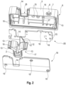
- Fig. 2 shows a housing of a clearer 10 in an exploded view.
- the housing may comprise at least a first housing part and a window carrier 17.
- the window carrier 17 is configured and arranged in a first configuration at the first housing part for a light from a light source 32 (see Fig. 4 to 6 for details) to pass at least one of a first window 89 for illuminating a guided yarn 34 or a second window 19 to pass the light from the guided yarn 34 to a receiver (see Fig. 4 to 6 for details) as described in detail elsewhere herein.
- the window carrier 17 can be configured to be detachable from the housing, particularly reversibly detachable from the housing, for transition to a second configuration, particularly for cleaning at least one window 19, 89.
- the housing may comprise a housing body 3 as first housing part and at least one PCBA 93. In some embodiments, as one is shown here, particularly a single PCBA 93 may be provided. Alternatively or additionally, a housing cover 18 may be provided as second housing part for covering and/or for sealing the housing body 3.
- the window carrier 17 may carry at least one window 89 on an emission side and at least one window 19 on a receiving side.
- a yarn guiding device 11 may be formed by the window carrier 17 to guide the yarn 34 in a position for illumination between the emission side and the receiving side, so through the measurement gap 9.
- the clearer 10 housing consist of 3 parts: the housing body 3, carrying the single PCBA 93 and the detachable part carrying the windows 19, 89 (wherein the detachable part is therefore referred to as window carrier 17), the housing cover 18, covering and sealing the housing body 3 as well as the detachable window carrier 17.
- the housing cover 18 is particularly attached to the housing body 3 by screws.
- the window carrier 17 may be held by compression as well as by form linkage between the housing body 3 and the housing cover 18.
- no individual, separate sealing compounds or seals e.g. made out of elastomers, silicons and or rubbers, are used to seal the parts contributing to the housing, other than a seal dome 7 for an optional button 8 and a connector seal 5 for the connector plug 6.
- no glue is used between the parts.
- no electronics are connected to the housing, particularly all electronics are provided on a single PCBA 93. All internal connections can preferably be made by using screws (not shown here) placed in screw holes 15.
- the whole housing including all the internal parts can be efficiently assembled with ease.
- ribs 27 allow to place the components in the right height and relative position inside the housing body 3, referred to as pockets 78 (see Fig. 11 ). Therefore, no special care may have to be taken during alignment, nor special thermal treatments may be needed for stress relief after assembly.
- the window carrier 17 can be easily exchanged by just removing and retightening a few screws. No re-calibration, no stress relief process may be required.
- the detachable window carrier 17 can also carry the eyelets 2 for guiding and stabilizing the yarn 34 in the measurement gap 9 (see Fig. 1 ) of the clearer 10.
- An alternative design may be to integrate the eyelets 2 into the housing body 3 for one part and into the housing cover 18 as the other part.
- Alignment structures 16 may provide the respective support to pre-align all components to be placed inside the housing body 3 upon assembly.
- the window carrier 17 comprises the windows 19, 89 as described elsewhere.
- the window carrier 17 may be placed in recesses 25 contacting a contact surface 14 for the window carrier 17 on the housing body 3 and similar contact surfaces 14 on the PCBA 93 and the housing cover 18.
- the window carrier 17 may interact with the housing body 3 via connector pins 13 and/or sleeves that form respective orthogonal sealing and locking features 83 as shown in Fig. 12B showing a cut view through a plane through the connector pins 13. It is understood that the connector pins 13 can be implemented pointwise as individual pins or pockets for location and or sleeves with a longitudinal shape covering location in combination with sealing.
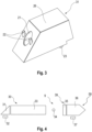
- Fig. 3 shows an illumination projector 30 with integrated mirror housing 31 functioning as a mirror holder for an exemplary embodiment of a waveguide 33 as shown in Fig. 4 .
- an exemplary illumination projector 30 design shows an 45° angle for second surface mirror attachment, wherein the offset correction for the thickness of the second surface mirror as mirror 21 as well as the heat stacks 22 are shown in Fig. 3 , to which the stamped mirror foil as mirror 21 can be placed and wherein heat stacks 22 can subsequently be molten to secure the mirror 21 in place.
- the LED as light source 32 is mounted in plane together with a receiving photodiode as photosensitive electronical component 37 on the PCB to form a PCBA 93, particularly being used for signal processing.
- the illumination projector 30 can have the light to be emitted by the light source 32, particularly in form of an LED, whereby the light source 32 is particularly mounted directly to the surface of the signal processing PCB, forming the PCBA 93, to particularly having a 90° angle of the illumination projection.
- the 90° illumination angle of the illumination projector 30 can be achieved by using a simple 45° mirror 21 added at the side of the light source 32, particularly the LED, to the waveguide 33, the waveguide 33 particularly being in form of a tube 26.
- a potential embodiment on mounting a mirror 21 together with the tube 26 as a single integrated component is shown in Fig. 3 .
- the 45° mirror 21 can be shaped and function as a prism (not shown), particularly using total reflection, or by adding a mirror coating at the 45° surface (as suggested in Fig. 4 ), by means of a simple first surface mirror (not shown) directly mounted to the illumination projector's 30 structure (not shown), or even simpler by means of a second surface mirror 21.
- An exemplary low cost means of integrating a mirror surface to the illumination projector 30 can be achieved by using a second surface mirror foil.
- the mirror foil can be particularly easily produced by stamping large sheets of abundantly available commercial mirror foils to the required size, particularly so as the surface mirror coating may be mechanically protected.
- the base materials used for these foils can be one of PE, PP or PMMA, all of which having low surface tensions compared to glass or aluminum.
- the low surface tension may be an inherent protection against vapor condensation. If so required, the already low surface tension can be further reduced by additional surface coatings on sheet basis.
- the thickness of the foils can be selected such, that the offset in the projection of the light (light bundle) of the second surface is negligible in practical terms, for instance by selecting secondary mirror foils with a thickness ranging from 0.05 to 0.15 mm. In case thicker foils are used, the offset by the secondary surface can be easily accommodated by correct optical arrangement of the actual waveguide 33, particularly in form of a projection tube 26 of the illumination projector's 30 structure.
- the secondary surface mirror can be secured to the illumination projector 30 using for instance glue. Direct gluing of the mirror 21 with particularly a low surface tension second surface to the illumination projector 30 can be avoided.
- a mechanical means of securing the mirror is for instance by means of a pocket in which the mirror 21 can be slit into following which the pocket being sealed off afterwards with i.e., glue. This is particularly done in production as additional sliders may be used during manufacturing of the illumination projector 30, but also the sliding of the mirror 21 into and the sealing of the pocket may be done. Moreover, the mirror 21 might get scratched during sliding into this pocket.
- Another alternative method may be applied by creating a box into which the mirror 21 can be placed followed by placing and/or pressing a cover into the box to be able to secure the mirror 21.
- box as well as cover are particularly to be provided.
- This is further simplified (further saving resources) by a method of heat staking: during injection molding heat stacks 22 can be made to the sidewall of the waveguide 33, particularly as a projection tube 26. As the secondary mirror foil can be stamped, holes can be made at the position of the heat stacks 22. During assembly the mirror 21 can be placed over the heat stacks 22 of the illumination projector 30. In the following the heat stacks 22 can be molten down to the lining of the mirror foil. The result is a low-cost production process that can have a very high yield, that is particularly clean and yields a secure mirror attachment regardless of environmental conditions and thermal cycling.
- the exit aperture of the waveguide 33 can be light absorbing (i.e. black).
- the end material may be non-specular and may have a shape that directs any light reflected off its surface away from the illumination receiving system 39 (which may be referred to as the receiver).
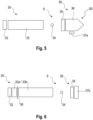
- Fig. 4 shows a schematic diagram of an exemplary embodiment of an optical setup.
- an illumination projector 30 is shown which is configured for a shadow projection from a yarn 34 in a textile machine.
- the illumination projector 30 may be configured for illuminating a yarn 34 for light to be reflected from the yarn 34.
- the illumination projector 30 may be independently implemented from an illumination receiving setup 39 as shown elsewhere herein.
- the illumination projector 30 particularly comprises at least one light source 32, particularly a light emitting diode or in short an LED.
- the illumination projector 30 particularly comprises at least one waveguide 33 and particularly a yarn guiding device 11.
- the light source 32 is particularly placed such that the emitted light enters the waveguide 33.
- the waveguide 33 is placed such that the light exiting the waveguide 33 particularly forms an area-source like emission on its exit side.
- the yarn guiding device 11 is particularly configured and positioned relative to the area-source like emission on the waveguide's 33 exit side to project a shadow from the yarn 34 to a receiving side or to reflect light from the yarn 34 to a receiving side.
- At the receiving side there may be one of different embodiments of an illumination receiving setup 39 as described elsewhere herein.
- the waveguide 33 comprises in particular a tube, further in particular, the tube is a light-homologation tube.
- the purpose of the light-homologation tube is to destroy any pattern or image carried in the propagating light beam e.g., an emitter pattern of an LED.
- the cross section of the tube contained in waveguide 33 can be of a round, elliptical, rectangular or squared shape. In longitudinal direction, the tube may be straight or conical.
- the cross section and the width of the waveguide 33 can be designed according to the required width of the light bundle and the height of the waveguide 33 can be designed according to the height requirement of the light bundle.
- the width of the waveguide 33 and the height of the waveguide 33 are individually and independently shaped according to the measurement requirements, wherein the width of the light bundle is adjusted to the width resolution e.g., of the yarn defects to be measured. They may correspond to the minimum length of the yarn defects to be detected.
- the height of the light bundle is particularly adjusted to the maximum size of the yarn defect to be measured.
- the waveguide 33 may comprise a hollow core with an inner surface being diffusive and/or non-specular. This way a maximum of light may be propagated through the waveguide in form of a tube, particularly a light-homologation tube while simultaneously destroying any pattern or image being carried in the light beam.
- Fig. 4 , 5 and 6 show different embodiments of the illumination projector 30, particularly considering the arrangement of the light source 32. Those may be combined freely with the different embodiments of an illumination receiving system 39 shown as matters of example.
- a shadow might be projected off from the yarn 34 into a direction of the receiving side. Additionally or alternatively, a light might be reflected off from the yarn 34 in other embodiments.
- the light propagation direction may be referenced as z-direction.
- the illumination receiving system 39 can be configured for receiving a shadow projection from a yarn 34 in a textile machine or it can be configured for receiving light reflected from the yarn 34.
- the illumination receiving system 39 particularly comprises at least one receiving cavity 36 and at least one photosensitive electronical component 37 to form a detector.
- the receiving cavity 36 can be configured and placed relative to a yarn 34 such that light emitted from a light source 32 and projecting a shadow from the yarn 34 and/or being reflected from the yarn 34 to enter the receiving cavity 36.
- the light entering the receiving cavity 36 can be transmitted to the at least one photosensitive electronical component 37 as a detector for measuring the incoming illumination.
- the photosensitive electronical component 37 may also be referenced as a detector. It may be capable of transferring the incoming radiation into an electronical signal which might be analyzed to determine at least one yarn 34 characteristic, such as composition, impurification, defects from yarn 34 formation, etc.
- An aperture 35 can be placed at the entrance of the receiving cavity 36.
- the aperture 35 may limit the light entering the receiving cavity 36, particularly in form of a lighthouse 59 to the light projecting the shadow or light being reflected from the yarn 34. Stray light or light from external light sources not included in the optical setup as described elsewhere herein, may be blocked by the aperture 35.
- At least the width of an aperture opening 42 of aperture 35 can be set to a range of a minimum length of the defect size of the yarn that is to be measured. Alternatively or additionally, at least the height of the aperture opening 42 of aperture 35 can be set to a range of a maximum defect size of the yarn that is to be measured.
- Opposite walls of the receiving cavity 36 may be at least diffusive, non-specular, shaped such that they direct light away from the aperture or are light absorbing in the wavelength range in which the at least one photosensitive electronical component 37 - the photosensitive detector - is sensitive.
- An aperture of the receiving cavity 36 - not to be mixed up with aperture 35 in the beam path in front of the receiving cavity 36 - may be light absorbing in the wavelength range in which the at least one photosensitive electronical component 37 is sensitive.
- the surface may be non-specular or shaped or positioned such that it directs light in a direction where potential secondary reflections back into the aperture of the receiving cavity 36 are minimal. This may prevent stray light to reach the photosensitive electronical component 37.
- At least one inner surface of the receiving cavity 36 comprises at least one of a non-specular surface finish or a highly reflective surface finish. This may improve the light propagation in the receiving cavity 36.
- both the light source 32 here in form of an LED and photosensitive electronical components 37 can be mounted in plane of the signal processing PCBA 93 (here not shown). This allows that all electrical components can be assembled during a single pass soldering process.
- the receiving photosensitive electronical component 37 e.g., a photodiode or other type of photosensitive detector, has no direct line of sight to the emitting LED.
- the illumination projector 30 may consist of a mere tube as waveguide 33.
- the following may also apply to waveguides 33 of different tape and structure e.g., glass fibers, photonic crystal fibers, etc.
- the tube is referenced as a mere example.
- the tube can be simple in structure and may not require special mechanical positioning tolerances, nor any special mechanical size tolerances.
- the tube can be manufactured as a simple part, i.e. by injection molding as described elsewhere herein. This allows to put a light source 32, particularly an LED, at one side of the tube and receive a light bundle at the other side of the tube with favorable properties of having particularly both: a low divergent angle, and an even distribution and/or no vignetting.
- the tube does not require tight mechanical manufacturing tolerances. In one embodiment it can be produced by extrusion and cut to the required length afterwards.
- the cross section of the tube can be varied according to the requirements: round, elliptical, rectangular, square etc. A particular shape may be elliptical as described in the following.
- the width of tube can be designed according to the desired width requirements of the light bundle and the height of the tube can be designed according to the desired height requirement of the light bundle.
- the width of the tube and the height of the tube can be individually and independently shaped according to the measurement requirements: the width of the light bundle is particularly adjusted to the width resolution of the yarn defects to be measured.
- the minimum length of the yarn defect to be detected may determine the width of the tube, whereas the height of the tube is adjusted to the maximum size of the yarn defect to be measured.
- the illumination flux of the light source 32 here the LED, increases according to the cross-section area of the tube, also to be referenced as projection tube.
- a projection tube with an elliptic shape may result in a higher illumination intensity, given the same emitted illumination flux of the light source 32, here the LED, compared to a round tube.
- the waveguide 33 as tube to form a projection tube is that the given design can avoid strict tolerances of the emission angle of the light source 32, particularly the LED, other than having a continuous first derivative of its projection profile. It does not even require to have the same angular emission profile in both axis, just a continuous first derivative in either axis.
- asymmetrical emission axes of the light source 32, particularly as LED these are oriented in accordance of the dimensions of the waveguide 33 as an illumination projector's 30 tube.
- the reduced requirements on the emission angles of the light source 32, particularly as LED allow for a much wider selection range. The wider selection range allows for additional cost optimization.
- the structure of the inner surface of the waveguide 33 as tube needs to be diffusive and/or non-specular.
- the length of the tube can (predominantly) determine the resulting divergence angle, whereas the preparation of the internal surface can determine the vignetting of the resulting light bundle.
- the efficiency of the projection is also determined by the reflective properties of the inner surface of the waveguide 33 as tube.
- This optical setup can avoid an out of plane arrangement of the electro-optical components (light source 32, particularly as LED, photosensitive electronical component 37 as detector, particularly at least one photodiode) with respect to the processing electronics.
- the electro-optical components light source 32, particularly as LED, photosensitive electronical component 37 as detector, particularly at least one photodiode
- the light source 32 particularly the LED
- the photosensitive electronical component 37 particularly the at least one photodiode
- they can be mounted on an additional flex-print (for each of them).
- a rigid-flex PCB or through-hole components may be used. All these embodiments carry additional costs and complexity during manufacturing.
- the embodiments described with respect to Fig. 4 can simplify part design and can improve tolerances in their production. Furthermore, assembly and part maintenance as well as service are improved.
- the illumination projector 30, producing a light bundle with even distribution (no vignetting) in combination with a low divergent angle may not be limited to the application of providing a yarn sensor for detecting at least one characteristic of a yarn 34, but can be used in any optical sensor for through light and/or reflective measurements.
- Fig. 5 shows a schematic diagram of an embodiment of an optical setup.
- the waveguide 33 is a mere tube as projection tube as well, but with direct attachment of the light source 32, here also an LED, by using a through hole LED component, or where an SMD LED is mounted to a flex print whereby the flex print is attached separately and independently to the signal processing PCBA 93 or where an SMD LED is mounted to the flex part of a rigid-flex board.
- an additional and individual mounting process of the light emitting part of the light source 32 to the waveguide 33 as a tube may be required.
- the receiving photo sensitive electronical components 37 have no direct line of sight to the light source 32 as an emitting LED. All the properties described with respect to Fig. 4 for the waveguide 33 as a tube, but also for other types of waveguides 33, remain, except for the 45° mirror 21 (see Fig. 3 ) in mirror housing 31.
- the light source 32 here the LED, is no longer mounted in plane of the signal processing PCBA 93. At least the light source 32, here the LED, and the waveguide 33 in form of a tube need to be pre-assembled before continuing with the assembly of the other housing parts.
- Figs. 4 and 5 it may particularly be possible to reduce the number of components for the illumination receiving system 39, being beneficial when the photosensitive electrical component 37 has no direct line of sight to the illumination projector 30 as illumination projection system. Without direct line of sight of the photosensitive electrical components 37 to the light emitting components, a diffusor 38 may not be required, as it is placed in the embodiment shown with respect to Fig. 6 .
- the photosensitive electrical component 37 can be placed in plane to the signal processing PCBA 93. Placing all the receiving photosensitive electrical components 37 on the same PCB (to form the PCBA 93) as the signal processing components, the electronics can be assembled in a cost conserving single manufacturing method step, as described elsewhere herein.
- the proposed exemplary solution can do both by using a lighthouse 59 as receiving cavity 36.
- the lighthouse 59 is a receiving cavity 36 in which all the light transmitted into it can be integrated by multiple reflections.
- the photosensitive electronical component 37 can be mounted to the side of the lighthouse 59 at a position where there is no direct line of sight to the incoming illumination entrapped by the lighthouse 59. This allows the photosensitive electronical component 37 to be placed in plane of the signal processing PCBA 93 without having a direct line of sight to the incoming illumination.
- the lighthouse 59 does not need to be pre-assembled to the single PCBA 93, but this can be done at a later stage in the assembly process as described elsewhere herein.
- the photosensitive electronical component 37 may measure the brightness of the entrapped incoming illumination by the lighthouse 59. Due to this indirect measurement, the size of the photosensitive electronical component can be decoupled and can thus be independent of the size of the object to be measured. This allows for selection of the most suitable photosensitive electronical component 37, with criteria being one or a combination of response time, sensitivity, wavelength range, sensitivity over wavelength, Noise Equivalent Power, active size, packaging type, cost, etc. This selection criteria may be much wider and allows for an improved optimization, where the first criteria to be met can be the maximum defect size that is to be measured.
- Fig. 6 shows a schematic diagram of an embodiment of an optical setup.
- the light source 32 as LED is no longer mounted in plane of the signal processing PCBA 93.
- an additional and individual mounting process of the light emitting part of the light source 32 to the waveguide 33 as tube is particularly required.
- At least the light source 32 as LED and the waveguide 33 as tube are particularly pre-assembled before continuing with the assembly of the other housing parts.
- the receiving photosensitive electronic component 37 can have a direct line of sight to the light source 32, particularly as emitting LED.
- the direct line of sight of the photosensitive electronical component 37 to the light source 32, particularly as LED, may require an additional diffusor 38 at the side of the light source 32. Without diffusor 38, the photosensitive electronical component 37 may look straight into the light source, here the LED, and be "blinded" by it.
- the contours of the light source 32 may be distinguished by the photosensitive electronical component 37 and may affect a uniform sensitivity of yarn defects over the measurement range over the aperture 35. This may be in analogy to a human looking straight into the sun or lamp.
- the diffusor 38 may be put immediately after the light source, particularly the LED, in z-direction when propagating from the light source 32.
- An alternative position can be at the side of the photosensitive electronical component 37, so in the illumination receiving system 39.
- the photosensitive electronical component 37 may be placed at the exit of the receiving aperture 35, results in inefficient use of the diffusor 38 with the risk of the contour of the light source 32, particularly the LED, may still be noticeable in the measurement field of the photosensitive electronical component 37.
- Putting the diffusor 38 immediately in front of the photosensitive electronical component 37 before the light bundle hits the photosensitive electronical component 37 may result in the contours of the light source 32, particularly the LED, to be still noticeable by the photosensitive electronical component 37.
- a tall detector 37b is used in accordance to the height of aperture 35.
- the length of the tall detector 37b may exceed the dimensions of the light beam hitting the aperture 35.
- a small detector 37a may be used which reduces the costs, but also may function at least partially as an aperture, particularly in addition to the aperture 35.
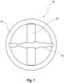
- Fig. 7 shows a schematic representation of an embodiment of an aperture 35 with passing yarn 34.
- the aperture 35 comprises a mounting ring 41 and an aperture opening 42 where the light passes through in z-direction from the light source 32 (here not shown, but see Figs. 4 to 6 for exemplary embodiments).
- the perspective is in z-direction, thus the light source 32 is behind the viewer.
- an aperture 35 can be placed at the entrance of the incoming light of the lighthouse 59, as shown in Figs. 4 to 6 .
- the width of the receiving aperture opening can be similar in range as the minimum length of the defect to be measured.
- the height of the aperture 35 can be in range of the maximum defect size that is to be measured.
- a thin aperture will allow light from all angles of the opening hemisphere to go through the aperture opening 42.
- a thin aperture has no angular blocking.
- a thin aperture is particularly not used as e.g., in the embodiments shown in Figs. 4 and 5 . Instead, for effective suppression of environmental light, the aperture 35 is such that it can reduce the opening angle over which light is to enter into the lighthouse 59.
- the receiving aperture 35 particularly reduces the opening angle of the lighthouse 59 over which light can be received.
- the exact calculation of the aperture opening dimensions of the lighthouse 59 can take the opening angle of the aperture 35 and the nominal distance of the yarn 34 to the aperture 35 into account.
- a thick aperture is used as aperture 35 as a simple-to-implement, low-cost solution.
- a mere mechanical aperture width of 1 mm and a depth of 4 mm- corresponding to the thickness - can have an opening angle of 28°. Any light bouncing off from the opposite wall of the illumination receiving system 39 in the direction of the lighthouse aperture 86 within the 28° reception conus can pass through the aperture 35.
- the embodiments can comprise a thick aperture in combination with anti-secondary reflective shapes of the lighthouse aperture 86 and of other opposing structures, particularly combined with a light-absorbing coating or respective light-absorbing materials of these structures.
- Fig. 8 shows a schematic ray diagram of an embodiment of an optical setup.
- a thin aperture 53 with lens assembly can be placed in front of the entrance of the receiving cavity 36 in an f-configuration for a shadow projection.
- the aperture opening 42 of aperture 35 is schematically represented as aperture diameter 51. Even though the aperture diameter 51 is referenced, the respective aperture opening 42 does not have to be round as described in detail elsewhere herein.
- alternative embodiments to those described with respect to Figs. 4 , 5 and 7 may combine a lens with a single aperture to further enhance the Signal to Noise ratio (S/N).
- a thin aperture with the desired sizes according to the defect to be measured can be in close spatial proximity to a focusing lens.
- the thin aperture together with the lens may form a thin aperture with lens assembly 53 which may be placed in a wall of the measurement gap 9, opposite to the illumination projector 30.
- the focal length of the lens can be selected such, that the focal length f is half the measurement gap width 54, the width of the measurement gap 9.
- the collimated light from the illumination projector 30 impinges onto the aperture 35 with lens assembly 53 and is focused by the lens on its focal point being placed inside the opening diameter 51 (the thin straight lines in Fig. 8 ).
- Stray light particularly originates from the yarn 34 may impinge onto the aperture and may be converted to a parallel (collimated) beam of light by the lens.
- Stray light originating from the outer bounds of the illumination projector objects 56 can pass the aperture with lens assembly 53 particularly having the same angle as that with which they were impinging.
- Stray light particularly originating from the center 55 of the illumination projector objects 56 (thick straight lines in Fig.
- the part holding the thin aperture with lens assembly 53 may be connected by a tube to the lighthouse 59, the interconnecting tube 58.
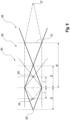
- Fig. 9 shows a schematic ray diagram of an embodiment of an optical setup.
- a thin aperture with lens assembly 53 can be placed in front of the entrance to the receiving cavity 36 in a greater than 2f configuration, particularly mounted in an interconnecting tube 58, for a reflection arrangement, particularly wherein the aperture opening size of the aperture of the receiving cavity 36 matches the aperture opening 42 size of the thin aperture of the thin aperture with lens assembly 53.
- the embodiment shown in Fig. 9 and described in the following increases Signal to Noise ratio (S/N).
- the reflective arrangement can use the same thin aperture with lens assembly 53 as was described with respect to the shadow projection arrangement from the embodiment depicted in Fig. 8 , but the entrance to the lighthouse 59 may be positioned at a distance further then 2f from the lens and the entrance 57 to the lighthouse 59 may have the same opening as the thin aperture, particularly the aperture diameter 51.
- the distance between the lighthouse 59 and the lens may be at least 4f.
- This light beam can pass the entrance to the lighthouse 59.
- Parallel (collimated light) back reflected from the opposite wall are, after passing the aperture of the aperture with lens assembly 53, focused to the secondary focus point 60 of the lens. Because of their steep angle, these rays can be absorbed by the walls of the interconnecting tube 58 between the lens and the entrance 57 of the lighthouse 59.
- Stray light, seemingly coming from the center 55 of the opposite wall (straight thick lines in Fig. 9 ) are, particularly after passing through the thin aperture, focused at a distance 2f from the lens by the lens of assembly 53. Because of the focus angle, this light spot will increase to the size of the thin aperture at distance 4f from the lens.
- the embodiments described can provide the means for implementing a method for projecting a shadow off from a yarn or for reflecting light off a yarn 34.
- the method may comprise the steps of providing light emitted by a light source 32. At least a part of the light emitted by the light source 32 may be collected in a waveguide in a method step. The light from the waveguide 33 may be transmitted to a yarn.
- the embodiments described can provide the means for implementing a method for measuring at least one characteristic in a yarn e.g., yarn defects.
- the method can comprise the step of emitting light from a light source 32 to a yarn 34 such that the light projects a shadow from the yarn 34 and/or the light reflects from the yarn 34.
- the light with the projected shadow or reflected from the yarn 34 can be collected in a receiving cavity 36.
- the light entering the receiving cavity 36 can be transmitted to at least one photosensitive electronical component 37 such that the incoming illumination is to be measured.
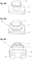
- Fig. 10A shows a top perspective view of an embodiment of a dual use light guide 70 with uses of signaling to the operator and the ability to provide operator feedback by means of a button press action.
- Light guide 70 consists of an operator activatable head 8 connected to a light guide shaft 71 for conducting light from a signaling light source, particularly a signaling LED (not shown).
- the light guide shaft 71 and head 8 are particularly placed on a basis 72, wherein the light guide shaft 71 particularly forms a shaft to transmit the force of pushing the head 8.
- head 8 is used for distribution of the light transmitted by light shaft 71 in a preferred direction to the operator, and in which basis 72 is used to efficiently collect light from the signaling LED (not shown).
- light guide 70 consisting of head 8, light shaft 71 and basis 72 and in which head 8, light guide shaft 71 and basis 72 are optically interconnected and constitute a single part.
- indicating lights can be used. These indicating lights can be implemented by one or multiple LED's.
- the LED's can have single color or consist of multiple colors.
- a typical intuitive color scheme when running may be green for OK and red for FAULT (corresponding to traffic light colors).
- An indication method may be implemented based on using blinking schemes of the LEDs used for indication.
- the blinking period and blinking scheme can indicate the state.
- the blinking scheme can extend to all the LED's available for indication use, conveying morse-type signs to the operator. Even though the messaging is less-intuitive as display communication and may take some initial training to get familiar with the morse-type code, its implementation is beneficial because of the variance of timing schemes. Moreover, LEDs are visible and distinguishable from a far distance. Furthermore, displays are more costly and more demanding in space, maintenance and implementation.
- a display using multiple LEDs or a couple of LEDs combined with a blinking scheme, particularly a signaling RGB LED is proposed by which the most important states can be easily indicated by intuitive color coding.
- RGB LED traffic light signaling as well as other states can be implemented.
- the number of states can be doubled, moreover closely related states or problems can be indicated by "color + non blinking” and "color + blinking".
- three different colors to indicate the amount of yarn 34 that is to be removed can be used.
- An alternative can be to choose a color in combination with a timing sequence to indicate the amount of yarn 34 that is to be removed.
- a positive scheme may indicate the amount of yarn that is to be removed
- a negative scheme may indicate that yarn is to be removed until all the yarn that is to be removed has been removed.
- “short blinking” may correspond to “short fault”, “little yarn to be removed”
- “middle period blinking” may correspond to “middle fault”
- “long period blinking” may correspond to "long fault”
- the signaling LED may keep indicating yarn to be removed for as long as there is still yarn to be removed.
- the signaling LED can be linked to a light guide 70.
- the shape of the light guide 70 may be such that it emits an elliptical illumination pattern: the emission flux side wards to the adjacent spindles are considerably larger compared to the emission angles in up (ceiling) and down (floor) direction. This emission pattern gives better visibility to the operator from far and reduces power consumption or necessity of LED loading to do so. Both improve efficiency.
- ellipsoidal Fresnel lenses or other structures impressed to the light emitting surface of button 8 (particularly its head) can be incorporated in addition to improve light distribution into the desired direction.
- Another feature for improvement of the light guide's 70 efficiency is to adapt the surface of the light guide 70 at the basis 72 where the light of the LED is coupled into, according to the emission profile of the signaling RGB LED and the desired light distribution i.e., typically domed as well, alternatively a conus shape.
- stopper 73 may be in place.
- stoppers 73 constraint the movement of the head in downwards direction to the side wall of the PCBA (not shown) and prevent over exerting pressure to a (micro) switch that is assembled to the same PCBA.
- the basis 72 may also engage with an LED, particularly in-between the stoppers 73, to couple light into the light guide shaft 71.
- the clearer 10 Besides indicating the state of the clearer 10 to the operator, often the clearer 10 (or its control system, control function and/or computer program products) desire to receive feedback from the operator, for instance in form of an acknowledgement or a confirmation that a certain corrective process or handling has been completed or can be initiated.
- a button 8 can be integrated into the clearer 10.
- the button 8 is particularly an additional component that can be placed onto the housing, particularly the housing body 3.
- provisions can be made for the button 8 to be holstered.
- the parts can be produced, assembled and checked.
- Integrating the button function together with the indicating light guide 70 can help reducing costs.
- a simple and robust alternative exemplary embodiment is that of a mechanical solution requiring the light guide 70 to be movable.
- the light guide 70 may be pushed down by the operator if so required and retracts on its own upon release.
- a mechanical solution is particularly independent of the means by which the button 8 is pressed.
- a mechanical solution is able to give tactile feedback to the operator pressing it.
- An alternative exemplary embodiment to a mechanical button 8 can be an all-optical solution.
- an additional photodiode may be used with which the variance in brightness of the returned or back-reflected light of the light guide 70 upon activation and/or blocking and/or reflection by the operators hand of the light guide 70 is measured.
- moving parts are avoided, which reduces mechanical maintenance requirements. Therefore, no tactile feedback can be given and the function may be dependent on environmental circumstances (sunlight exposure).
- Fig. 10B shows a top perspective view of an exemplary embodiment of a button 8 with a seal dome 7.
- the light guide 70 can be capable to move down when being pressed by the operator and can be capable to retract on its own upon release.
- the spring-loaded action for the light guide 70 to retract on its own can be implemented by the sealing.
- the sealing may comprise a seal dome 7, which compresses when being pressed which results in storing energy in a material deformation used to return to its original shape when released.
- the tactile feedback can be achieved by activating a micro-switch at the end of the stroke of the light guide 70.
- a mechanical stopper 73 may be integrated into the PCBA 93 (here not shown) to which the tactile switch is assembled.
- the stopper 73 By implementation of the stopper 73 on the same PCBA 93 as the tactile switch, all tolerances can be controlled during PCBA 93 manufacturing particularly reducing cost and increasing accuracy. Introduction of tolerances during assembly or other tolerance stack ups can thus be avoided.
- a basis 72 can be integrated as a flange underneath the button and/or the light guide that is significantly wider compared to the opening in the housing body 3 where the button 8 or the button with seal dome 7 is to be implemented.
- the light guide 70 and/or button 8 can be assembled together with its seal dome 7 from the inside of the housing prior to assembly of the PCBA 93.
- the button 8 to the outside is constrained by the housing body 3 and to the inside by the PCBA 93 (after its assembly).
- buttons 8 can inadvertently be removed from the housing body 3 e.g., by a fingernail gripping in the seam (not shown) between housing body 3 and button 8 or between seal dome 7 and housing body 3.
- Fig. 10D shows a partial cut view of an exemplary embodiment of a seal dome 7 for a button 8 as described with respect to Figs. 10A to 10C .
- the seal particularly comprises a hollow core 74 that can be configured and positioned for the light guide 70 to be incorporated therein.
- the button 8 can be surrounded in a circumferential direction by the seal dome 7.
- a spring part 75 can support the spring action by deforming upon pressing the button 8, storing energy in the material deformation to return to the original unpressed configuration upon release of the pressure on the button 8.
- a seal basis 76 can be provided to insulate the button 8 and/or the light guide 70 mechanically and electronically from the PCBA 93 (not shown).
- Fig. 10E shows a button 8 with seal dome 7 surrounding it, placed as button with light guide 70 at a housing body 3.
- the perspective view is onto the bottom of the housing, where the housing cover 18 is sunk into the housing body 3 as described elsewhere herein.
- a screw is shown being located in a screw hole 15 to compress the housing cover 18 into the housing body 3, forming a seam 77.
- the button may be positioned such that it protrudes on a sidewall of the housing body 3 when placed in textile machine.
- Fig. 11 shows a cut view through a plane parallel to the yarn propagation direction and parallel to a z-direction through a housing.
- the window carrier 17 can be held by compression between the housing body 3 and the housing cover 18 forming a linkage between the housing body 3 and the housing cover 18.
- the linkage particularly comprises no sealing compound or seal which seals the parts contributing to the housing.
- the linkage particularly comprises no glue which glues the parts contributing to the housing.
- no electronics are connected to the housing.
- the embodiment depicted in Fig. 11 comprises a sealing that is a combination between form consistent part design and a meandering sealing.
- the housing cover 18 may comprise a gravity seal. To do so, the clearer 10, the housing body 3 and the housing cover 18 are configured such that the housing cover 18 may be arranged at the bottom of the clearer 10, latest when implemented into a textile machine for operation. In addition, the housing cover 18 is particularly sunk into the housing body 3. Therefore, there are particularly no cover seams 77 to the side of the housing body 3 only underneath as shown in Fig. 10E for matter of example. By close form fit of the housing cover 18 to the sidewalls of the housing body 3, a first seal can be created. By placing the housing cover 18 at the bottom and sunken into the housing body 3, all dust falling in direction of gravity, cannot enter into the housing, because of gravity (gravity seal).
- a double meandering sealing 79 with form fit can be employed.
- dust would have to move up (against gravity) between the housing body's 3 side wall 69 and housing cover 18, particularly up to a first recess of the housing cover 18. There, the dust would have to move horizontally between housing body 3 and housing cover 18 until reach a first wall 90.
- the same sealing technique can be employed for sealing the window carrier 17 to the housing body 3 at the top as well as sealing to the housing cover 18 at the bottom.
- sealing of the window carrier 17 to the front or to the stern side of the clearer an even more elaborate meandering seal is implemented: by using two orthogonal sealing features as shown in Fig. 12B .
- the dust would have to move first sideways to the back of the clearer 10 and/or of the housing body 3, then horizontally to the side of the housing body 3, followed by a forwards movement, followed by again a horizontal movement, then followed by a repeated movement to the back of the housing after which another horizontal stretch needs to be passed followed by a third movement to the back succeeded by fourth horizontal movement and a fourth movement to the back after which a reversed sideways stretch is to be passed and then a final fifth movement to the back.
- This is also shown in the Fig. 2 , where the window carrier 17 is shown from a top angled view. In this and alternative embodiments several angles as well as reversed motion directions are provided. These angles and reversed motions do not have to be full U-turns as described above.
- Fig. 12A shows a cut view through a first plane perpendicular to the yarn propagation direction through a housing showing a selected part thereof.
- Fig. 12B shows a cut view through a second plane perpendicular to the yarn propagation direction through a housing showing a selected part thereof.
- Fig. 12A and Fig. 12B meandering sealings are shown that block dust from entering the housing body 3 due to a form fit between the housing body 3 and Window Carrier 17 and housing cover 18.
- Fig. 12A refers to the double meandering sealing 79 as described with respect to Fig. 11 , just in a bottom view, not in a cut view.
- the gravity seal can be formed by the housing cover 18 (here not shown) sunken into the housing body 3 to be oriented such that the housing cover 18 forms the bottom of the housing.
- several angles as well as reversed motion directions are provided. These angles and reversed motions do not have to be full up-down-turns as described above.
- several different angles can be chosen and also several meandering length of the path provided for the dust to pass. The particular scheme may be provided such that it achieves the desired dust protection rating.
- Fig. 12B shows the stern side sealing arrangement with orthogonal locking and sealing arrangement 83 that forms a meandering seal as described already with respect to Fig. 11 for the window carrier 17.
- Fig. 12B shows the stern side sealing arrangement with orthogonal locking and sealing arrangement 83 that forms a meandering seal as described already with respect to Fig. 11 for the window carrier 17.
- several angles as well as reversed motion directions are provided. These angles and reversed motions do not have to be full U-turns as described above.
- several different angles can be chosen and also several meandering length of the path provided for the dust to pass. The particular scheme may be provided such that it achieves the desired dust protection rating.
- the individual and independent elastomer seal would undergo aging of the material.
- the material might lose elasticity when compared to the elasticity it had during production. It potentially also provides sticking issues to a housing part, etc.
- the individual and independent seal upon opening of the housing, the individual and independent seal, although visibly in shape, might have lost at least some level of its former elasticity which causes a risk after re-tightening of the housing.
- Fig. 13A shows a cut view through a first plane perpendicular to the yarn propagation direction through a housing shown in full, partially assembled.
- Fig. 13B shows an embodiment of a window carrier 17 with an embodiment of a lighthouse 59.
- eyelets 2 can guide and stabilize the yarn 34 in a measurement gap 9 of a clearer 10.
- the eyelets 2 may be placed in the window carrier 17.
- the eyelets 2 can be placed at the housing body 3 for one part and at the housing cover 18 as the other part.
- Fig. 13C shows an embodiment of a lighthouse 59.
- Fig. 13D shows a cut view through a first plane perpendicular to the yarn propagation direction through a housing shown in full, partially assembled with an optical setup placed therein.
- Figs. 13A to 13D show a partial representation of a method of assembling a housing in their respective order.
- the point of view is from a bottom into the housing body 3.
- the housing cover 18 is not sunk into the bottom of the respective housing body 3, yet.
- the step of placing optical components in a housing body as shown in Fig. 13A and concluded in Fig. 13D is shown.
- the button 8 as button with light guide 70 may be placed into a fitting hole in the housing body 3 and sealed using the seal dome 7 with seal basis 76.
- the placing of the optical components can be followed by placing a PCBA 93 in the housing body 3, further followed by a step of connecting the optical components and the PCBA 93.
- the window carrier 17 can be placed in the housing body 3 as shown in Fig. 13A .
- the lighthouse 59 is shown in Fig. 13 C in isolation.
- a holder 80 may provide a screw hole 15 to screw the lighthouse 59 to the PCBA 93 at a later stage during assembly.
- An alignment pin 87 provides the necessary alignment, particularly together with the ribs 27 as they were shown in Figs. 12A and 12B for example to align the optical as well as the electronical components.
- the PCBA 93 may place in the alignment pin 87 and thus align receiving photo sensitive electronical component 37 (here not shown as the PCBA 93 is not in place).
- the housing particularly has no individual and separate sealing component or seals made out of elastomers, silicons and or rubbers the housing can be assembled or disassembled multiple times and particularly because of using only screws, the assembly or disassembly can be done with ease. Together with the undercut of the housing forming pockets 78 as shown and explained with respect to Fig. 11 , no special alignment has to be performed. Furthermore, no aging processes take place. This allows for completion of the complete assembly in one go. As the whole assembly can be done at a single stage, this saves valuable floor space in the production facility. Moreover it can save on production effort: No part is handled twice. This saves further resources. As an additional benefit, the assembly process facilities automation during production.
- all electronics are on at least one PCBA 93, particularly a single PCBA 93.
- Alignment structures 16 can align the PCBA 93 with the optical components.
- the alignment tolerances of the waveguide 33 as projector tube and lighthouse 59 with aperture 35 are accommodating. This may avoid the need of a special alignment procedure other than mounting them to the same plane on the PCBA 93 and particularly ensuring general alignment by placement of pinholes in the mounting plane PCBA 93.
- the alignment by alignment structures 16 on the PCBA 93, but also by the ribs 27 and the formed pockets 78, the optical components such as the waveguide 33 and/or the lighthouse 59 can be placed such that they already align with the PCBA 93 before it is even introduced to the housing body 3.
- a beam entrance 88 of the waveguide may align with the light source 32 (not shown), while a beam exit 85 of the lighthouse 59 may align with the photosensitive electronical component 37 (not shown in Fig. 13D ).
- the optical components can be placed individually into the housing body 3 first and only connected to the PCBA 93 after the PCBA 93 has been assembled into the housing body 3. This reverses any assembly process where PCBA 93 and optics are assembled to a sub-module first.
- the optics are placed into the housing body first (after the button 8 is placed, but this can be independently performed, unless it is placed before the PCBA 93 is placed).
- This allows to implement undercuts as pockets 78 (see Fig. 11 ) in the housing body for placement of the optical components.
- This in turn allows for independent optimization of the design of the optical components and the sealing design of the housing as was described in detail herein with respect to Figs. 11 to 12B .
- the housing cover 18 is sunk into the housing body 3, particularly following a step of placing the PCBA 93.
- the method for assembly of a housing or a clearer may comprise the following steps:
- the housing can be placed in an assembly fixture.
- the sealing 5 for the connector 6 and/or sealing dome 7 for button 8 can be inserted, followed by inserting the light guide 70 and/or button 8.
- These steps can also be reversed.
- the window carrier 17 may be put together with the illumination receiving system 39 as an insertion combination into the housing body 3 (sliding and pressing the window carrier 17 into the housing body 3: light compression may exist, even though it is not screwed in yet). During this process normal production cleanliness can be sufficient. Windows 19, 89 of the window carrier 17 can be checked on obvious dirt / smear prior to insertion.
- Sub-assemblies may be provided in that the lighthouse aperture 86 may be pushed into the lighthouse 56 and in that the eyelets 2 may be heat staked to the window carrier 17.
- the illumination projector 30 as assembly may be put into the housing body 3.
- the illumination projector 30 as assembly can be checked on cleanliness and that no foreign particles, no scratches and no deformations are present in the waveguide 33, particularly in form of a tube. Photodiode and LED holes can be checked that they are open, not blocked, no flashes etc. are present.
- Sub-assemblies may be provided e.g., by pushing the projector aperture to the illumination projector's 30 core of the waveguide 33 being a tube and/or by heat staking of the mirror 21 to the illumination projector's 30 core of the waveguide 33 being a tube.
- the connector seal 5 into the housing body 3 to implement the connector plug 6. In all these steps one may ensure that the corners of the components and sub-assemblies are seated correctly.
- the PCBA 93 (not shown here) may be slid (from the right or from the bottom) into the housing body 3. In a step it may be taken care of that the seating of the connector seal 5 is placed correctly.
- the illumination projector 30 (projector) and illumination receiving system 39 (receiver) using may be screwed to the housing body using at least one screw each, particularly by using only a single screw each.
- one may take care of a correct alignment of each of the pins to the PCBA 93.
- the PCBA 93 may be secured to the housing body 3, particularly by using at least a single screw, particularly by using only a single screw.
- the housing cover 18 is sunk into a bottom of the housing body and may be secured, particularly with 3 screws.
- a preferred method for manufacturing of the projection tube is particularly by (direct) injection molding, particularly without secondary inner surface conditioning processes, like secondary grinding (machining) or coating of the inner surface of the waveguide 33 being a tube.
- a draft angle may be provided for secure tool release of the inner pin shaping the inner surface and its structure. Suitable draft angles can range between 1 and 10 degrees. Depending on the cross section of the inner tube and the desired structure the draft angle can range between 3 and 7 degrees. The inclusion of the draft angle can have a minimal influence on the divergence angle of the exit beam and particularly only a minor can have an influence on the intensity of the exit light bundle.
- the material choice may affect the efficiency of the embodiment.
- the material can allow for an inherently non-specular and highly reflective (90 % or higher, preferably 99 % or higher) surface finish.
- the non-specular surface requirement can be influenced by the surface finish of the molding tool and by the properties of the material used (filler properties).
- a material that is highly reflective and non-directional reduces the requirements to be given for the emitted illumination flux of the light source 32, particularly the LED.
- a material providing very high reflective properties and being non directional can be is Barium Sulfate (BaSO 4 ).
- Manufacturing of the lighthouse 59 can be performed by direct injection molding (particularly no secondary processes like machining and or coating of the inner surface of the lighthouse 59).
- the light entrapped by the lighthouse 59 can be integrated by multiple non-specular reflections as described elsewhere herein.
- the material choice of the lighthouse 59 can affect the efficiency of the embodiment resulting from the method.
- the material can have an inherently non-specular and highly reflective surface finish.
- the non-specular surface requirement is influenced by the surface finish of the molding tool and by the properties of the material used (filler properties).
- a material that is highly reflective and non-directional increases the illumination efficiency.
- a material providing very high reflective properties and being non directional can be Barium Sulfate (BaSO 4 ).
- Barium Sulfate can be provided as a powder. When sprayed directly to a surface it can easily be rubbed off. Therefore, Barium Sulfate can be added to a coating (for instance latex with 50% weight/weight also in short w/w), improving its rubbing fastness. Providing barium sulfate in a coating can be achieved by submitting the receiving cavity 36 for secondary processing. Secondary processing of the receiving cavity 36 might add undesirable costs during manufacturing.
- Barium Sulfate pigments can be added to a base plastic compound and by extruding this mixture. The resulting granulate can be used for injection molding in method steps described elsewhere herein.
- Precipitated Barium Sulfate may be used as a delivery component.
- the filler can be mixed with the base material of choice, like i.e., PA or ABS.
- Barium Sulfate as a filler can add further properties to the base material. It may improve processability, hardness, and chemical resistance.
- Titanium Dioxide (TiOz) can be used as a highly reflective filler for a plastic compound.
- a material can be selected that has highly absorptive properties.
- a material with a high carbon content can be highly absorptive over a wide wavelength range.
- when used as a filler in a plastic compound it may render this compound conductive.
- adding carbon as a filler to the material choice for the aperture may reduce environmental and stray light sensitivity and may also improve EMV and ESD susceptibility.
- the term “may” refers to optional features of the invention. Consequently, there are also further aspects and/or embodiments of the invention which additionally or alternatively have the respective feature or features. All features in feature combinations are also disclosed independently thereof and may also be singled out from the combinations of features disclosed herein and used in combination with other features to specify the subject-matter of the any of the claims, dissolving any structural and/or functional relationship that may exist between the features. Terms like “first”, “second”, “third” may be used to refer to a list of elements, but does not necessarily describe these features or elements according to their importance, their order of appearance or importance. Therefore, these elements or features may specify the different aspects in any other particular order, unless explicitly expressed.
Landscapes
- Physics & Mathematics (AREA)
- Health & Medical Sciences (AREA)
- Life Sciences & Earth Sciences (AREA)
- Chemical & Material Sciences (AREA)
- Analytical Chemistry (AREA)
- Biochemistry (AREA)
- General Health & Medical Sciences (AREA)
- General Physics & Mathematics (AREA)
- Immunology (AREA)
- Pathology (AREA)
- Engineering & Computer Science (AREA)
- Textile Engineering (AREA)
- Investigating Materials By The Use Of Optical Means Adapted For Particular Applications (AREA)
Applications Claiming Priority (1)
| Application Number | Priority Date | Filing Date | Title |
|---|---|---|---|
| LU505551A LU505551B1 (en) | 2023-11-16 | 2023-11-16 | Illumination receiving system and method for measuring |
Publications (1)
| Publication Number | Publication Date |
|---|---|
| EP4556896A1 true EP4556896A1 (de) | 2025-05-21 |
Family
ID=89321622
Family Applications (1)
| Application Number | Title | Priority Date | Filing Date |
|---|---|---|---|
| EP24211215.9A Pending EP4556896A1 (de) | 2023-11-16 | 2024-11-06 | Beleuchtungsempfangssystem und messverfahren |
Country Status (3)
| Country | Link |
|---|---|
| EP (1) | EP4556896A1 (de) |
| CN (1) | CN120009174A (de) |
| LU (1) | LU505551B1 (de) |
Citations (9)
| Publication number | Priority date | Publication date | Assignee | Title |
|---|---|---|---|---|
| GB484426A (en) * | 1936-09-30 | 1938-05-05 | Karl Strippel | Process for the production of reflectors for lighting purposes, and metal strips, mouldings or the like, for building and other purposes |
| JPH0473702A (ja) * | 1990-07-16 | 1992-03-09 | Mitsui Petrochem Ind Ltd | 拡散反射体 |
| US5414520A (en) * | 1992-03-17 | 1995-05-09 | Zellweger Uster Ag | Process and device for detecting impurities in a textile test material |
| EP0572592B1 (de) * | 1991-12-20 | 1997-06-04 | Zellweger Luwa Ag | Fremdfasererkennung in garnen |
| EP0761585B1 (de) * | 1995-09-06 | 2000-02-02 | Zellweger Luwa Ag | Garnsensor |
| EP1508797B1 (de) * | 2003-08-21 | 2008-12-17 | Murata Kikai Kabushiki Kaisha | Detektionsvorrichtung für Fremdstoffe in Garnen |
| EP1655599B1 (de) | 2004-11-06 | 2012-09-19 | Oerlikon Textile GmbH & Co. KG | Garnsensor |
| US20190182440A1 (en) * | 2017-12-13 | 2019-06-13 | The Hong Kong Research Institute Of Textiles And Apparel Limited | Multispectral color imaging device based on integrating sphere lighting and calibration methods thereof |
| US20210199593A1 (en) * | 2017-09-14 | 2021-07-01 | Uster Technologies Ag | Fiber Blend Identification and Ratio Measurement |
-
2023
- 2023-11-16 LU LU505551A patent/LU505551B1/en active IP Right Grant
-
2024
- 2024-11-06 EP EP24211215.9A patent/EP4556896A1/de active Pending
- 2024-11-15 CN CN202411635717.3A patent/CN120009174A/zh active Pending
Patent Citations (9)
| Publication number | Priority date | Publication date | Assignee | Title |
|---|---|---|---|---|
| GB484426A (en) * | 1936-09-30 | 1938-05-05 | Karl Strippel | Process for the production of reflectors for lighting purposes, and metal strips, mouldings or the like, for building and other purposes |
| JPH0473702A (ja) * | 1990-07-16 | 1992-03-09 | Mitsui Petrochem Ind Ltd | 拡散反射体 |
| EP0572592B1 (de) * | 1991-12-20 | 1997-06-04 | Zellweger Luwa Ag | Fremdfasererkennung in garnen |
| US5414520A (en) * | 1992-03-17 | 1995-05-09 | Zellweger Uster Ag | Process and device for detecting impurities in a textile test material |
| EP0761585B1 (de) * | 1995-09-06 | 2000-02-02 | Zellweger Luwa Ag | Garnsensor |
| EP1508797B1 (de) * | 2003-08-21 | 2008-12-17 | Murata Kikai Kabushiki Kaisha | Detektionsvorrichtung für Fremdstoffe in Garnen |
| EP1655599B1 (de) | 2004-11-06 | 2012-09-19 | Oerlikon Textile GmbH & Co. KG | Garnsensor |
| US20210199593A1 (en) * | 2017-09-14 | 2021-07-01 | Uster Technologies Ag | Fiber Blend Identification and Ratio Measurement |
| US20190182440A1 (en) * | 2017-12-13 | 2019-06-13 | The Hong Kong Research Institute Of Textiles And Apparel Limited | Multispectral color imaging device based on integrating sphere lighting and calibration methods thereof |
Also Published As
| Publication number | Publication date |
|---|---|
| CN120009174A (zh) | 2025-05-16 |
| LU505551B1 (en) | 2025-05-19 |
Similar Documents
| Publication | Publication Date | Title |
|---|---|---|
| US8405636B2 (en) | Optical position sensing system and optical position sensor assembly | |
| US9121567B2 (en) | Turn lamp for vehicle outside mirror | |
| CN109813425B (zh) | 一种光源光功率检测装置及激光光源 | |
| US6285782B1 (en) | Mounting apparatus, recognition device and recognition method for electronic component | |
| JP2009538737A (ja) | キャリア材料上における溶接部の画像を評価する装置 | |
| US20070165232A1 (en) | Optical sensor device | |
| CN112711089B (zh) | 一种杂散光遮蔽结构、包含其的超微距成像模块 | |
| US5012115A (en) | Device for optically detecting hold position of electronic component with dual emitters | |
| AU733167B2 (en) | Light projection device for a photoelectric smoke sensor | |
| EP4556896A1 (de) | Beleuchtungsempfangssystem und messverfahren | |
| LU505549B1 (en) | Illumination projector, method of manufacturing and method of projection | |
| LU505548B1 (en) | Housing and method of assembly | |
| JP6220672B2 (ja) | 変位センサ | |
| CN111580325A (zh) | 一种高亮转角同轴光源 | |
| CN216560302U (zh) | 接触式图像传感器 | |
| CN113746996B (zh) | 接触式图像传感器 | |
| CN219831828U (zh) | 读码器 | |
| CN219496698U (zh) | 光纤传感器 | |
| EP1026496A1 (de) | Optischer Koppler für Feuchtigkeitssensor | |
| CN216313192U (zh) | 接触式图像传感器 | |
| US20040228103A1 (en) | Lighting apparatus | |
| US20250052931A1 (en) | Optical Device With Stray Light Reduction | |
| KR101191230B1 (ko) | 곡면 촬영을 위한 산업용 조명유닛 | |
| CN120253684A (zh) | 一种边缘检测系统和照明装置 | |
| US20210243326A1 (en) | Lighting device and image reading device |
Legal Events
| Date | Code | Title | Description |
|---|---|---|---|
| PUAI | Public reference made under article 153(3) epc to a published international application that has entered the european phase |
Free format text: ORIGINAL CODE: 0009012 |
|
| STAA | Information on the status of an ep patent application or granted ep patent |
Free format text: STATUS: THE APPLICATION HAS BEEN PUBLISHED |
|
| AK | Designated contracting states |
Kind code of ref document: A1 Designated state(s): AL AT BE BG CH CY CZ DE DK EE ES FI FR GB GR HR HU IE IS IT LI LT LU LV MC ME MK MT NL NO PL PT RO RS SE SI SK SM TR |
|
| STAA | Information on the status of an ep patent application or granted ep patent |
Free format text: STATUS: REQUEST FOR EXAMINATION WAS MADE |
|
| 17P | Request for examination filed |
Effective date: 20251121 |