EP4557505A1 - Millimeterwellen-führung und übertragungssystem mit einer solchen millimeterwellen-führung - Google Patents
Millimeterwellen-führung und übertragungssystem mit einer solchen millimeterwellen-führung Download PDFInfo
- Publication number
- EP4557505A1 EP4557505A1 EP24213168.8A EP24213168A EP4557505A1 EP 4557505 A1 EP4557505 A1 EP 4557505A1 EP 24213168 A EP24213168 A EP 24213168A EP 4557505 A1 EP4557505 A1 EP 4557505A1
- Authority
- EP
- European Patent Office
- Prior art keywords
- waveguide
- millimeter
- signal
- millimeter wave
- transmission
- Prior art date
- Legal status (The legal status is an assumption and is not a legal conclusion. Google has not performed a legal analysis and makes no representation as to the accuracy of the status listed.)
- Pending
Links
Images




Classifications
-
- H—ELECTRICITY
- H01—ELECTRIC ELEMENTS
- H01P—WAVEGUIDES; RESONATORS, LINES, OR OTHER DEVICES OF THE WAVEGUIDE TYPE
- H01P5/00—Coupling devices of the waveguide type
- H01P5/12—Coupling devices having more than two ports
-
- H—ELECTRICITY
- H01—ELECTRIC ELEMENTS
- H01P—WAVEGUIDES; RESONATORS, LINES, OR OTHER DEVICES OF THE WAVEGUIDE TYPE
- H01P3/00—Waveguides; Transmission lines of the waveguide type
- H01P3/16—Dielectric waveguides, i.e. without a longitudinal conductor
-
- H—ELECTRICITY
- H01—ELECTRIC ELEMENTS
- H01P—WAVEGUIDES; RESONATORS, LINES, OR OTHER DEVICES OF THE WAVEGUIDE TYPE
- H01P5/00—Coupling devices of the waveguide type
- H01P5/02—Coupling devices of the waveguide type with invariable factor of coupling
Definitions
- the present application relates to a millimeter waveguide made of a dielectric material and a millimeter wave transmission system comprising such a waveguide.
- millimeter waves It is known to transmit millimeter waves through a dielectric plastic waveguide. For some applications, it is desirable to be able to transmit millimeter waves corresponding to the aggregation of several millimeter waves in different frequency bands, each corresponding to a signal to be transmitted.
- FIG. 1 is a diagram showing an example of a millimeter wave transmission system 5.
- the millimeter wave transmission system 5 comprises a millimeter wave transmitting device 10, a millimeter wave receiving device 30, and a waveguide 20 made of dielectric plastic material transmitting the millimeter electromagnetic waves between the transmitting device 10 and the receiving device 30.
- the millimeter wave receiving device 30 comprises a millimeter wave receiving antenna 31 capturing the millimeter electromagnetic waves supplied by the waveguide 20 and supplying a reception signal SRG in the transmission band ⁇ B.
- the receiving device 30 further comprises a distribution circuit 32 receiving the analog reception signal SRG and supplying M analog reception signals SR 1 to SR M to M reception blocks 33 1 to 33 M , M being an integer between 1 and 8 typically, but possibly being a higher integer, M being equal to 3 for example in Figure 1 .
- Each reception block 33 j , j varying from 1 to M comprises a demodulation circuit 34 j receiving the reception signal SR j and providing an SBR signal j in the final frequency band.
- a disadvantage of the millimeter wave transmission system 5 of the Figure 1 is that the generation of the overall analog STG signal can have significant losses.
- a disadvantage of the millimeter wave transmission system 5 of the Figure 1 is that good coupling between the waveguide 20 and each antenna 31 and 35 may be difficult to implement over the entire bandwidth transmission frequencies ⁇ B which can be higher than several tens of GHz.
- An embodiment overcomes all or part of the disadvantages of millimeter waveguides made of a dielectric material and of millimeter wave transmission systems comprising such a known waveguide.
- One embodiment provides a millimeter waveguide comprising a first portion connected to a second portion, the first portion comprising first waveguides, each configured to receive a first millimeter wave, and the second portion corresponding to a second waveguide, each first waveguide comprising a first free end and a second end joined to the second waveguide, each first and second waveguide being entirely made of a dielectric material.
- the millimeter waveguide further comprises a third portion comprising third waveguides, each third waveguide comprising a first free end and a second end joined to the second waveguide.
- the first and second waveguides each comprise a tube delimiting an internal volume filled with a gas, a mixture of gases, a fluid or a solid whose dielectric constant is lower than that of the dielectric material.
- the dimensions of the straight sections of the first waveguides are different.
- the cross section of the tube of at least one of the first waveguides is rectangular and the cross-section of the second waveguide tube is circular.
- the first and second waveguides are each made of a plastic material, in particular polytetrafluoroethylene, polypropylene or polystyrene.
- An embodiment also provides a system for transmitting first millimeter waves comprising a millimeter waveguide as defined above, a millimeter wave transmission device and a millimeter wave reception device, the millimeter wave transmission device comprising, for each first waveguide, an antenna configured for the transmission of millimeter waves and coupled with said first waveguide.
- each first millimeter wave has a frequency band between 30 GHz and 300 GHz.
- the frequency bands of the first millimeter waves are distinct.
- a millimeter wave is an electromagnetic wave whose wavelength can vary between 1 mm and 10 mm, which corresponds to a frequency that can vary between 30 GHz and 300 GHz.
- FIG. 2 is a diagram showing one embodiment of a millimeter wave transmission system 40.
- the millimeter wave transmission system 40 comprises all of the elements of the millimeter wave transmission system 5 shown in Figure 1 with the difference that the combination circuit 14, the antenna 15, the antenna 31, and the distribution circuit 32 are not present, that the transmission device 10 comprises an antenna 42 i for each transmission block 11 i , i varying from 1 to N, that the reception device 30 comprises an antenna 44 j for each reception block 33 j , j varying from 1 to M, and that the waveguide 20 is replaced by a waveguide 50.
- Each transmission block 11 i , i varying from 1 to N, and the corresponding antenna 42 i then forms a transmission circuit 45 i of millimeter waves in a transmission frequency band ⁇ B i .
- the waveguide 50 comprises a first part also called the collection part 51, a second part 52, and a third part also called the distribution part 53.
- the central waveguide 52 connects the collection part 51 to the distribution part 53.
- the collection part 51 comprises N branches 54 1 to 54 N (three branches 54 1 , 54 2 , and 54 3 being represented as example in Figure 2 ).
- Each branch 54 2 i varying from 1 to N, corresponds to a first waveguide.
- the second part 52 corresponds to a second waveguide and called central waveguide thereafter.
- Each branch 54 i i varying from 1 to N, comprises a free end 55 i and is connected, on the side opposite the free end 55 i , to the central waveguide 52.
- the distribution part 53 comprises M branches 56 1 to 56 M (three branches 56 1 , 56 2 , and 56 3 being represented in Figure 2 ). Depending on the application envisaged, the number M may be equal to N or different from N.
- Each branch 56 j , j varying from 1 to M corresponds to a third waveguide which comprises a free end 57 j and which is connected, on the side opposite the free end 57 j , to the central waveguide 52.
- the waveguide 50 is entirely made of a dielectric material.
- the waveguide 50 does not comprise any electrically conductive elements, in particular metallic elements. This advantageously makes it possible to produce a flexible waveguide 50, in particular one exhibiting elastic deformations.
- Each antenna 42 i i varying from 1 to N, is arranged in proximity, preferably in contact with the axial end 55 2 of the branch 54 i .
- Each antenna 42 i is for example adapted to emit millimeter waves which propagate in the corresponding branch 54 i .
- Each antenna 42 i is adapted to emit a millimeter wave in the transmission frequency band ⁇ B i .
- the millimeter wave in the transmission frequency band ⁇ B i propagates in the branch 54 i to the central waveguide 52.
- the millimeter waves add up at the junction between each branch 54 i and the central waveguide 52 to form a millimeter wave in the frequency band of transmission ⁇ B.
- Each antenna 44 j , j varying from 1 to M, is arranged in proximity, preferably in contact with the axial end 57 j of the branch 56 j .
- Each antenna 44 j is for example adapted to capture millimeter waves which propagate in the corresponding branch 56 j .
- the aggregation of millimeter waves in the transmission frequency bands ⁇ B i is carried out by the waveguide 50 while for the system 5 of the Figure 2 , this aggregation is carried out on the signals ST i by the combination circuit 14 of the transmission device 10.
- the aggregation of the millimeter waves in the transmission frequency bands ⁇ B i can, advantageously, be carried out with fewer losses, in particular insertion losses, by the waveguide 50 than when it is carried out by the combination circuit 14.
- the distribution of millimeter waves in the transmission frequency bands ⁇ B i is carried out by the waveguide 50 while for the system 5 of the Figure 2 , this distribution is carried out on the signals ST i by the distribution circuit 32 of the reception device 30.
- the distribution of the millimeter waves in the transmission frequency bands ⁇ B i can, advantageously, be carried out with fewer losses, in particular insertion losses, by the waveguide 50 than when it is carried out by the distribution circuit 32.
- the signals ST i , i varying from 1 to N correspond to different signals.
- the transmission frequency bands ⁇ B i can then be distinct and the transmission frequency band ⁇ B can correspond to the sum of the transmission frequency bands ⁇ B i .
- the width of the transmission frequency band ⁇ B is then greater than the width of each transmission frequency band ⁇ B i .
- the width of each transmission frequency band ⁇ B i may be less than 10 GHz.
- the transmission device 10 may provide signals ST 1 , ST 2 , ST 3 , and ST 4 , the signal ST 1 being in the frequency band ⁇ B 1 from 122 GHz to 131 GHz, the signal ST 2 being in the frequency band ⁇ B 2 from 131 GHz to 140 GHz, the signal ST 3 being in the frequency band ⁇ B 3 from 140 GHz to 149 GHz, and the signal ST 4 being in the frequency band ⁇ B 4 from 149 GHz to 157 GHz.
- the width of each frequency band ⁇ B 1 , ⁇ B 2 , ⁇ B 3 , and ⁇ B 4 is equal to 9 GHz.
- the millimeter waves transported in the central waveguide 52 are then in the frequency band ⁇ B from 122 GHz to 157 GHz.
- the width of the frequency band ⁇ B is equal to 35 GHz.
- the efficiency of the coupling between a millimeter waveguide and an antenna depends in particular on the width of the frequency band of the millimeter waves to be transmitted to the waveguide. Therefore, the coupling between each antenna 42 i and the branch 54 i for the system 40 of the Figure 2 , which is to be carried out on the frequency band ⁇ B i , can, advantageously, be more efficient than the coupling between the antenna 15 and the waveguide 20 for the system 5 of the Figure 2 which is to be carried out on the wider ⁇ B frequency band.
- the signals ST i are identical.
- the transmission frequency bands ⁇ B i can then be substantially identical and the transmission frequency band ⁇ B can be substantially equal to the transmission frequency band ⁇ B i .
- Such an application makes it possible to generate a high-power millimeter wave transported by the central waveguide 52 from reduced-power millimeter waves emitted by each antenna 42 i , i varying from 1 to N.
- the propagation mode of the electromagnetic waves in the waveguide 50 is different from the transverse electromagnetic mode, also called TEM mode.
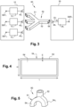
- FIG. 3 is a diagram showing one embodiment of a millimeter wave transmission system 60.
- the millimeter wave transmission system 60 comprises all of the elements of the millimeter wave transmission system 40 shown in Figure 2 with the difference that the reception device 30 comprises a single reception block 33 1 , and that the waveguide 50 does not comprise the distribution part 53, the central guide 52 comprising an end 58 located opposite the antenna 44 1 of the reception block 33 1 .
- This embodiment can in particular be implemented in the case where the transmission frequency bands ⁇ B i are substantially identical and the transmission frequency band ⁇ B.
- the branch 54 1 comprises a tube 62 made of a dielectric plastic material delimiting an internal volume 64.
- the internal volume 64 can be filled with a gas or a gaseous mixture, for example air, or with a liquid or solid dielectric material whose dielectric constant can be lower than that of the dielectric material making up the tube 62.
- the internal volume 64 is filled with air.
- the tube 62 is surrounded by a sheath, not shown in Figure 4 , made of a dielectric material whose dielectric constant is lower than that of the dielectric material making up the tube 62.
- the branch 54 1 comprises a solid rod of the dielectric plastic material.
- the tube 62 or the solid rod has a substantially rectangular cross-section or circular, other cross-sectional shapes nevertheless being conceivable (for example, an elliptical cross-section).
- the tube 62 or the solid rod has a substantially rectangular cross-section which promotes the propagation of millimeter waves in the TE10 mode.
- the tube 62 or the rod has a substantially rectangular cross-section having a width L and a height H.
- the width L is between 0.5 mm and 10 mm.
- the height H is between 0.25 mm and 5 mm.
- the thickness E of the wall of the tube 62 is between 0.5 mm and 10 mm.
- the dielectric constant of the dielectric material forming the tube 62 or the rod of the branch 54 1 is for example between 1 and 4, preferably between 2 and 4.
- the loss angle or delta tangent of the dielectric material forming the tube 62 or the rod of the branch 54 1 is for example less than 10 -3 to ensure minimal signal losses in the branch 54 1 .
- This material may be a dielectric plastic material such as for example polytetrafluoroethylene, polypropylene or polystyrene.
- the wavelength of the electromagnetic waves propagating in the branch 54 1 is between 7 mm and 0.7 mm.
- waves at a frequency of around 60 GHz can be used, for which, for a material with a dielectric constant of 2, the wavelength is 3.5 mm.
- Each branch 54 2 to 54 N may have the same characteristics as those previously described for branch 54 1 .
- Each branch 56 1 to 56 M may have the same characteristics as those previously described for branch 54 1 .
- the central waveguide 52 may have the same characteristics as those described previously for branch 54 1 .
- the dimensions of the straight sections of the branches 54 1 to 54 N are different.
- the dimensions of the straight section of the branch 54 i are adapted to the frequency band ⁇ B i of the millimeter waves transported by the branch 54 i .
- the dimensions of the straight sections of the branches 54 1 to 54 N are identical.
- the dimensions of the straight sections of the branches 56 i to 56 M are different.
- the dimensions of the straight sections of the branch 56 j are adapted to the frequency band of the millimeter waves to be processed by the reception block 33 j associated with the branch 56 j .
- the dimensions of the straight sections of the branches 56 i to 56 M are identical.
- the shape (for example circular shape, rectangular shape, etc.) of the cross section of the central waveguide 52 is different from the shape of the cross section of the branches 54 1 to 54 N .
- FIG. 5 is a partial and schematic perspective view of an embodiment of the waveguide 50 whose collection part 51 comprises two branches 54 1 and 54 2 , the number of branches 54 i however being able to be greater than 2, each having a rectangular cross-section and whose central waveguide 52 has a circular cross-section.
- the waveguide 52 can have a length greater than the length of each branch 54 1 and 54 2 and the manufacture on an industrial scale of a waveguide having a circular cross-section is simpler than the manufacture of a guide of waves having a rectangular cross section.
- Each branch 54 1 , 54 2 having a rectangular cross section which receives a millimeter wave supplied by the associated antenna 42 1 , 42 2 makes it possible to reduce losses during the capture by the branch 54 1 , 54 2 of the millimeter wave emitted by the associated antenna 42 1 , 42 2 .
- the 50 waveguide can be a single piece or obtained by assembling several pieces.
- FIG. 6 is a partial and schematic perspective view of an embodiment of the waveguide 50 whose collection part 51 comprises two branches 54 1 and 54 2 , the number of branches 54 i however being able to be greater than 2, and which corresponds to a separate part of the central waveguide 52.
- the manufacturing methods of the central waveguide 52 and of the collection part 51 can then be different.
- the central waveguide 52 can be manufactured by extrusion and the collection part 51 can be manufactured by molding.
- FIG. 7 and the figure 8 are respectively a top view and a side view, partial and schematic, illustrating the connection between the waveguide 50 and the transmission device 10 according to one embodiment.
- the Figure 9 and the Figure 10 are figures analogous respectively to the Figure 7 and to the figure 8 illustrating the connection between the waveguide 50 and the transmission device 10 according to another embodiment.
- the collection part 51 of the waveguide 50 comprises two branches 54 1 and 54 2 , the number of branches 54 i however being able to be greater than 2.
- the transmission device 10 comprises, for example, a printed circuit 70 and at least one microprocessor 72 mounted on the printed circuit 70.
- the antennas 42 1 and 42 2 are formed by conductive tracks 74 of the printed circuit 70, the antennas 42 1 and 42 2 being represented by dotted lines in Figure 9 .
- the waveguide 50 is mounted according to a so-called edge coupling.
- the antennas 42 1 and 42 2 are formed along an edge 76 of the printed circuit 70 and the branches 54 1 and 54 2 of the waveguide 50 are arranged along the edge 76 so that the axis of each branch 54 1 , 54 2 at the end 55 1 , 55 2 is substantially parallel to the plane of the printed circuit 70.
- Each antenna 42 1 , 42 2 may be in contact with the end 55 1 , 55 2 of the corresponding branch 54 1 , 54 2 .
- the waveguide 50 is mounted according to a so-called vertical coupling.
- the branches 54 1 and 54 2 of the waveguide 50 are arranged so that the axis of each branch 54 1 , 54 2 at the end 55 1 , 55 2 is substantially perpendicular to the plane of the printed circuit 70.
- Each antenna 42 1 , 42 2 can be covered by the corresponding branch 54 1 , 54 2 .
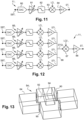
- FIG. 11 is a block diagram of an embodiment of a transmission block 11 i , i varying from 1 to N, in which the transmission block 11 i receives a single digital signal SBT i , and performs modulation to provide the SMT signal in the transmission frequency band ⁇ B i .
- FIG. 12 is a block diagram of another embodiment of a transmission block 11 i , i varying from 1 to N.
- the transmission block 11 i receives several digital signals SBT i and performs a first modulation to provide an analog signal STI i in an intermediate frequency band.
- the transmission block 11 i then provides an analog signal STGI i equal to the sum of the analog signals STI i and then performs a second modulation from the signal STG i to provide the signal ST i in the transmission frequency band ⁇ B i .
- this filtering function is performed directly by the waveguide 50.
- the filtering function can be implemented on each branch 54 i , on the central waveguide 52, and/or on each branch 56 j .
- the filtering function is implemented by providing the branch 54 i , the central waveguide 52, and/or the branch 56 j with a cross section that varies along the branch 54 i , the central waveguide 52, and/or the branch 56 j .
- FIG. 13 is a perspective, partial and schematic view of the internal volume 64 of the branch 54 1 illustrating the performance of a filtering function by the branch 54 1 .
- the cross section of the branch 54 1 comprises abrupt variations, for example one or more constriction zones 90 in which the cross section of the branch 54 1 is reduced, one or more expansion zones 92 in which the cross section of the branch 54 1 is increased, and/or one or more obstacles 94 on the path of the millimeter waves.
- the system 40 of the Figure 2 can be used in full duplex mode, the transmitting device 10 then further comprising a millimeter wave receiving device, for example analogous to the receiving device 30, and the receiving device 30 further comprising a millimeter wave transmitting device, for example analogous to the receiving device 10, so that millimeter waves can be transported by the waveguide 50 in both directions.
Landscapes
- Control Of Motors That Do Not Use Commutators (AREA)
- Waveguides (AREA)
Applications Claiming Priority (1)
| Application Number | Priority Date | Filing Date | Title |
|---|---|---|---|
| FR2312646A FR3155645A1 (fr) | 2023-11-17 | 2023-11-17 | Guide d'ondes millimetriques et systeme de transmission comprenant un tel guide d'ondes |
Publications (1)
| Publication Number | Publication Date |
|---|---|
| EP4557505A1 true EP4557505A1 (de) | 2025-05-21 |
Family
ID=90811050
Family Applications (1)
| Application Number | Title | Priority Date | Filing Date |
|---|---|---|---|
| EP24213168.8A Pending EP4557505A1 (de) | 2023-11-17 | 2024-11-15 | Millimeterwellen-führung und übertragungssystem mit einer solchen millimeterwellen-führung |
Country Status (3)
| Country | Link |
|---|---|
| US (1) | US20250167418A1 (de) |
| EP (1) | EP4557505A1 (de) |
| FR (1) | FR3155645A1 (de) |
Citations (3)
| Publication number | Priority date | Publication date | Assignee | Title |
|---|---|---|---|---|
| US20060035585A1 (en) * | 2004-08-16 | 2006-02-16 | Sony Corporation | Distributing apparatus and method for communication using the same |
| US20200076042A1 (en) * | 2010-07-02 | 2020-03-05 | Cubic Corporation | Three-dimensional microstructures |
| US20230344106A1 (en) * | 2022-04-22 | 2023-10-26 | Raytheon Company | Waveguide-to-waveguide power combiner/divider |
Family Cites Families (2)
| Publication number | Priority date | Publication date | Assignee | Title |
|---|---|---|---|---|
| US8988294B2 (en) * | 2011-12-06 | 2015-03-24 | Viasat, Inc. | Antenna with integrated condensation control system |
| US9478843B2 (en) * | 2014-02-19 | 2016-10-25 | California Institute Of Technology | Dielectric waveguides splitter and hybrid/isolator for bidirectional link |
-
2023
- 2023-11-17 FR FR2312646A patent/FR3155645A1/fr active Pending
-
2024
- 2024-11-09 US US18/942,577 patent/US20250167418A1/en active Pending
- 2024-11-15 EP EP24213168.8A patent/EP4557505A1/de active Pending
Patent Citations (3)
| Publication number | Priority date | Publication date | Assignee | Title |
|---|---|---|---|---|
| US20060035585A1 (en) * | 2004-08-16 | 2006-02-16 | Sony Corporation | Distributing apparatus and method for communication using the same |
| US20200076042A1 (en) * | 2010-07-02 | 2020-03-05 | Cubic Corporation | Three-dimensional microstructures |
| US20230344106A1 (en) * | 2022-04-22 | 2023-10-26 | Raytheon Company | Waveguide-to-waveguide power combiner/divider |
Also Published As
| Publication number | Publication date |
|---|---|
| FR3155645A1 (fr) | 2025-05-23 |
| US20250167418A1 (en) | 2025-05-22 |
Similar Documents
| Publication | Publication Date | Title |
|---|---|---|
| EP0604338B1 (de) | Wenig Raum beanspruchende, breitbandige Antenne mit zugehörigem Sendeempfänger | |
| EP2223377B1 (de) | Radiale Vorrichtung zur Leistungsverstärkung mit Phasensdispersionausgleich der Verstärkungswege | |
| EP1172885A1 (de) | Kurzgeschlossene Streifenleiterantenne und Zweiband-Übertragungsanordnung damit | |
| EP0426972A1 (de) | Ebene Antenne | |
| FR3105884A1 (fr) | Cornet pour antenne satellite bi-bande Ka à polarisation circulaire | |
| EP3726642B1 (de) | Polarisationsschirm mit breitband-hochfrequenz-polarisationszelle(n) | |
| EP0880193B1 (de) | Antennenstrahler für Mikrowellensendung und empfang | |
| EP2195877B1 (de) | Omt-breitband- und multiband-/sende- und empfangs-/kopplungs- und trennvorrichtung für hochfrequenz-telekommunikationsantennen | |
| EP3136499B1 (de) | Aufteilungs-/kombinationssystem für hyperfrequenzwelle | |
| FR2850793A1 (fr) | Transition entre un circuit micro-ruban et un guide d'onde et unite exterieure d'emission reception incorporant la transition | |
| FR2850792A1 (fr) | Filtre compact en guide d'onde | |
| WO2022069806A1 (fr) | Connecteur radiofrequence | |
| EP4557505A1 (de) | Millimeterwellen-führung und übertragungssystem mit einer solchen millimeterwellen-führung | |
| EP0015610B1 (de) | Spiegelfrequenzreflektierendes Mikrowellenfilter und Mikrowellenempfänger mit einem solchen Filter | |
| EP0015838B1 (de) | Breitbändiger Hochfrequenzmischer | |
| EP0153541A1 (de) | Rundes Fernster für einen Mikrowellenhohlleiter | |
| EP1152483B1 (de) | Zweiband-Mikrowellenstrahlelement | |
| FR2742262A1 (fr) | Filtre pseudo-elliptique dans le domaine millimetrique realise en technologie guide d'ondes | |
| EP3293815A1 (de) | Millimeter-wellenleiter | |
| FR2463520A1 (fr) | Reseau quadriporte pour la separation de deux signaux constitues par des bandes de frequences a double polarisation | |
| FR2935198A1 (fr) | Element rayonnant compact a faibles pertes | |
| EP0430136A1 (de) | Bandsperrfilter für Mikrowellenhohlleiter | |
| WO2024189480A1 (fr) | Transducteur orthomode compact bi-bande à polarisation linéaire | |
| EP3537541B1 (de) | Elektromagnetische entkoppelung | |
| WO2024047573A1 (fr) | Jonction orthomode à six ports |
Legal Events
| Date | Code | Title | Description |
|---|---|---|---|
| PUAI | Public reference made under article 153(3) epc to a published international application that has entered the european phase |
Free format text: ORIGINAL CODE: 0009012 |
|
| STAA | Information on the status of an ep patent application or granted ep patent |
Free format text: STATUS: REQUEST FOR EXAMINATION WAS MADE |
|
| 17P | Request for examination filed |
Effective date: 20241115 |
|
| AK | Designated contracting states |
Kind code of ref document: A1 Designated state(s): AL AT BE BG CH CY CZ DE DK EE ES FI FR GB GR HR HU IE IS IT LI LT LU LV MC ME MK MT NL NO PL PT RO RS SE SI SK SM TR |