EP4560403A1 - Appareil de formation d'images - Google Patents
Appareil de formation d'images Download PDFInfo
- Publication number
- EP4560403A1 EP4560403A1 EP24211067.4A EP24211067A EP4560403A1 EP 4560403 A1 EP4560403 A1 EP 4560403A1 EP 24211067 A EP24211067 A EP 24211067A EP 4560403 A1 EP4560403 A1 EP 4560403A1
- Authority
- EP
- European Patent Office
- Prior art keywords
- charging
- transfer
- photosensitive member
- image forming
- forming apparatus
- Prior art date
- Legal status (The legal status is an assumption and is not a legal conclusion. Google has not performed a legal analysis and makes no representation as to the accuracy of the status listed.)
- Pending
Links
Images


Classifications
-
- G—PHYSICS
- G03—PHOTOGRAPHY; CINEMATOGRAPHY; ANALOGOUS TECHNIQUES USING WAVES OTHER THAN OPTICAL WAVES; ELECTROGRAPHY; HOLOGRAPHY
- G03G—ELECTROGRAPHY; ELECTROPHOTOGRAPHY; MAGNETOGRAPHY
- G03G21/00—Arrangements not provided for by groups G03G13/00 - G03G19/00, e.g. cleaning, elimination of residual charge
- G03G21/06—Eliminating residual charges from a reusable imaging member
-
- G—PHYSICS
- G03—PHOTOGRAPHY; CINEMATOGRAPHY; ANALOGOUS TECHNIQUES USING WAVES OTHER THAN OPTICAL WAVES; ELECTROGRAPHY; HOLOGRAPHY
- G03G—ELECTROGRAPHY; ELECTROPHOTOGRAPHY; MAGNETOGRAPHY
- G03G15/00—Apparatus for electrographic processes using a charge pattern
- G03G15/50—Machine control of apparatus for electrographic processes using a charge pattern, e.g. regulating differents parts of the machine, multimode copiers, microprocessor control
- G03G15/5004—Power supply control, e.g. power-saving mode, automatic power turn-off
-
- G—PHYSICS
- G03—PHOTOGRAPHY; CINEMATOGRAPHY; ANALOGOUS TECHNIQUES USING WAVES OTHER THAN OPTICAL WAVES; ELECTROGRAPHY; HOLOGRAPHY
- G03G—ELECTROGRAPHY; ELECTROPHOTOGRAPHY; MAGNETOGRAPHY
- G03G15/00—Apparatus for electrographic processes using a charge pattern
- G03G15/02—Apparatus for electrographic processes using a charge pattern for laying down a uniform charge, e.g. for sensitising; Corona discharge devices
- G03G15/0208—Apparatus for electrographic processes using a charge pattern for laying down a uniform charge, e.g. for sensitising; Corona discharge devices by contact, friction or induction, e.g. liquid charging apparatus
- G03G15/0216—Apparatus for electrographic processes using a charge pattern for laying down a uniform charge, e.g. for sensitising; Corona discharge devices by contact, friction or induction, e.g. liquid charging apparatus by bringing a charging member into contact with the member to be charged, e.g. roller, brush chargers
-
- G—PHYSICS
- G03—PHOTOGRAPHY; CINEMATOGRAPHY; ANALOGOUS TECHNIQUES USING WAVES OTHER THAN OPTICAL WAVES; ELECTROGRAPHY; HOLOGRAPHY
- G03G—ELECTROGRAPHY; ELECTROPHOTOGRAPHY; MAGNETOGRAPHY
- G03G15/00—Apparatus for electrographic processes using a charge pattern
- G03G15/02—Apparatus for electrographic processes using a charge pattern for laying down a uniform charge, e.g. for sensitising; Corona discharge devices
- G03G15/0266—Arrangements for controlling the amount of charge
-
- G—PHYSICS
- G03—PHOTOGRAPHY; CINEMATOGRAPHY; ANALOGOUS TECHNIQUES USING WAVES OTHER THAN OPTICAL WAVES; ELECTROGRAPHY; HOLOGRAPHY
- G03G—ELECTROGRAPHY; ELECTROPHOTOGRAPHY; MAGNETOGRAPHY
- G03G15/00—Apparatus for electrographic processes using a charge pattern
- G03G15/02—Apparatus for electrographic processes using a charge pattern for laying down a uniform charge, e.g. for sensitising; Corona discharge devices
- G03G15/0283—Arrangements for supplying power to the sensitising device
-
- G—PHYSICS
- G03—PHOTOGRAPHY; CINEMATOGRAPHY; ANALOGOUS TECHNIQUES USING WAVES OTHER THAN OPTICAL WAVES; ELECTROGRAPHY; HOLOGRAPHY
- G03G—ELECTROGRAPHY; ELECTROPHOTOGRAPHY; MAGNETOGRAPHY
- G03G15/00—Apparatus for electrographic processes using a charge pattern
- G03G15/14—Apparatus for electrographic processes using a charge pattern for transferring a pattern to a second base
- G03G15/16—Apparatus for electrographic processes using a charge pattern for transferring a pattern to a second base of a toner pattern, e.g. a powder pattern, e.g. magnetic transfer
- G03G15/1665—Apparatus for electrographic processes using a charge pattern for transferring a pattern to a second base of a toner pattern, e.g. a powder pattern, e.g. magnetic transfer by introducing the second base in the nip formed by the recording member and at least one transfer member, e.g. in combination with bias or heat
- G03G15/167—Apparatus for electrographic processes using a charge pattern for transferring a pattern to a second base of a toner pattern, e.g. a powder pattern, e.g. magnetic transfer by introducing the second base in the nip formed by the recording member and at least one transfer member, e.g. in combination with bias or heat at least one of the recording member or the transfer member being rotatable during the transfer
- G03G15/1675—Apparatus for electrographic processes using a charge pattern for transferring a pattern to a second base of a toner pattern, e.g. a powder pattern, e.g. magnetic transfer by introducing the second base in the nip formed by the recording member and at least one transfer member, e.g. in combination with bias or heat at least one of the recording member or the transfer member being rotatable during the transfer with means for controlling the bias applied in the transfer nip
-
- G—PHYSICS
- G03—PHOTOGRAPHY; CINEMATOGRAPHY; ANALOGOUS TECHNIQUES USING WAVES OTHER THAN OPTICAL WAVES; ELECTROGRAPHY; HOLOGRAPHY
- G03G—ELECTROGRAPHY; ELECTROPHOTOGRAPHY; MAGNETOGRAPHY
- G03G15/00—Apparatus for electrographic processes using a charge pattern
- G03G15/14—Apparatus for electrographic processes using a charge pattern for transferring a pattern to a second base
- G03G15/16—Apparatus for electrographic processes using a charge pattern for transferring a pattern to a second base of a toner pattern, e.g. a powder pattern, e.g. magnetic transfer
- G03G15/1665—Apparatus for electrographic processes using a charge pattern for transferring a pattern to a second base of a toner pattern, e.g. a powder pattern, e.g. magnetic transfer by introducing the second base in the nip formed by the recording member and at least one transfer member, e.g. in combination with bias or heat
- G03G15/167—Apparatus for electrographic processes using a charge pattern for transferring a pattern to a second base of a toner pattern, e.g. a powder pattern, e.g. magnetic transfer by introducing the second base in the nip formed by the recording member and at least one transfer member, e.g. in combination with bias or heat at least one of the recording member or the transfer member being rotatable during the transfer
- G03G15/1685—Structure, details of the transfer member, e.g. chemical composition
-
- G—PHYSICS
- G03—PHOTOGRAPHY; CINEMATOGRAPHY; ANALOGOUS TECHNIQUES USING WAVES OTHER THAN OPTICAL WAVES; ELECTROGRAPHY; HOLOGRAPHY
- G03G—ELECTROGRAPHY; ELECTROPHOTOGRAPHY; MAGNETOGRAPHY
- G03G21/00—Arrangements not provided for by groups G03G13/00 - G03G19/00, e.g. cleaning, elimination of residual charge
- G03G21/0005—Arrangements not provided for by groups G03G13/00 - G03G19/00, e.g. cleaning, elimination of residual charge for removing solid developer or debris from the electrographic recording medium
- G03G21/0064—Arrangements not provided for by groups G03G13/00 - G03G19/00, e.g. cleaning, elimination of residual charge for removing solid developer or debris from the electrographic recording medium using the developing unit, e.g. cleanerless or multi-cycle apparatus
-
- G—PHYSICS
- G03—PHOTOGRAPHY; CINEMATOGRAPHY; ANALOGOUS TECHNIQUES USING WAVES OTHER THAN OPTICAL WAVES; ELECTROGRAPHY; HOLOGRAPHY
- G03G—ELECTROGRAPHY; ELECTROPHOTOGRAPHY; MAGNETOGRAPHY
- G03G2215/00—Apparatus for electrophotographic processes
- G03G2215/00953—Electrographic recording members
- G03G2215/00957—Compositions
-
- G—PHYSICS
- G03—PHOTOGRAPHY; CINEMATOGRAPHY; ANALOGOUS TECHNIQUES USING WAVES OTHER THAN OPTICAL WAVES; ELECTROGRAPHY; HOLOGRAPHY
- G03G—ELECTROGRAPHY; ELECTROPHOTOGRAPHY; MAGNETOGRAPHY
- G03G2215/00—Apparatus for electrophotographic processes
- G03G2215/00953—Electrographic recording members
- G03G2215/00962—Electrographic apparatus defined by the electrographic recording member
Definitions
- the present invention relates to an image forming apparatus, such as a printer, a copying machine, or a facsimile machine, using an electrophotographic type.
- the image forming apparatus such as a laser printer, of the electrophotographic type
- a surface of a photosensitive member is electrically charged by a charging means, and the charged surface of the photosensitive member is exposed to light by an exposure means (image developing position), so that an electrostatic latent image is formed on the photosensitive member.
- toner is deposited on the electrostatic latent image by a developing means, so that a toner image is formed on the photosensitive member, and this toner image is transferred onto a sheet-like recording material by a transfer means.
- a rotatable photosensitive drum is used in many cases.
- a transfer member such as a transfer roller for forming a transfer portion in contact with the photosensitive member is used in many cases.
- an image forming apparatus including the photosensitive drum and the transfer roller will be described as an example.
- a toner image on the photosensitive drum is transferred from the photosensitive drum onto the recording material under application of a transfer voltage of an opposite potential to a charge polarity of the photosensitive drum to the transfer roller.
- the charge polarity (normal charge polarity) of the photosensitive drum is a polarity of a potential formed on a surface of the photosensitive drum charged by the charging means for image formation.
- the transfer memory occurs and the surface of the photosensitive drum is non-uniformly charged, when the surface of the photosensitive drum is subsequently charged by the charging means, it is difficult to uniformize a surface potential of the photosensitive drum in some instances.
- the transfer memory As a condition in which the transfer memory is liable to occur, in the case of an image forming apparatus of a direct transfer type in which the toner image is directly transferred from the photosensitive member onto the recording material, it is possible to cite a state in which the transfer voltage is not applied to the transfer roller in a state that the recording material is not interposed between the photosensitive drum and the transfer roller.
- the recording material which is an electric resistor is not interposed between the photosensitive drum and the transfer roller, when a transfer voltage similar to a transfer voltage when the recording material is interposed between the photosensitive drum and the transfer roller is applied to the transfer roller, the electric discharge is liable to occur between the photosensitive drum and the transfer roller in some cases.
- Japanese Laid-Open Patent Application No. 2016-218155 discloses an image forming apparatus in which a pre-exposure means (pre-charging exposure means) for exposing the surface of the photosensitive drum, immediately after passing through the transfer portion, to light is provided.
- the surface potential of the photosensitive drum on which the transfer memory generated is, for example, the same in polarity as the charge polarity of the photosensitive drum and becomes lower in absolute value than a potential after the image exposure, even when the surface of the photosensitive drum is exposed to light by the above-described pre-exposure means, it is difficult to uniformize a potential of a portion where an absolute value of a surface potential has already become lower than the potential after the image exposure. Further, it would be also considered that exposure intensity of the pre-exposure means is made stronger than exposure intensity of the exposure means for performing the image exposure. However, particularly, in the case where at least part of the surface potential of the photosensitive drum on which the transfer memory generated is reversed in polarity to the opposite polarity to the charge polarity (charge potential), it is difficult to sufficiently uniformize the transfer memory.
- a principal object of the present invention is to provide an image forming apparatus capable of suppressing occurrence of an image defect due to a transfer memory.
- an image forming apparatus comprising: a rotatable photosensitive member; a first charging member configured to electrically charge a surface of the photosensitive member in contact with the surface of the photosensitive member in a first charging position with respect to a rotational direction of the photosensitive member; a second charging member configured to electrically charge the surface of the photosensitive member in a second charging position with respect to the rotational direction of the photosensitive member; a developing member configured to form a toner image on the surface of the photosensitive member by supplying toner, charged to a predetermined polarity, to the surface of the photosensitive member in a developing position with respect to the rotational direction of the photosensitive member; a transfer member contacting the surface of the photosensitive member in a transfer position with respect to the rotational direction of the photosensitive member and configured to transfer the toner image from the photosensitive member onto a recording material passing through between the photosensitive member and the transfer member; a first charging voltage applying portion configured to apply a first charging voltage of the predetermined
- FIG. 1 is a schematic sectional view of an image forming apparatus 100 of an embodiment 1.
- the image forming apparatus 100 of this embodiment is a laser beam printer of an electrophotographic type and is capable of forming a black (monochromatic) image on a recording material P depending on image information inputted from an external device 200 such as a personal computer.
- an external device 200 such as a personal computer.
- the image forming apparatus 100 includes a photosensitive drum 1 which is drum-shaped (cylindrical) photosensitive member as an image bearing member inside an apparatus main assembly.
- the photosensitive drum 1 is constituted by providing a photosensitive material, such as OPC (organic photosensitive member, organic photoconductor), amorphous selenium, or amorphous silicon on a cylindrical drum substrate formed of aluminum, nickel, or the like.
- OPC organic photosensitive member, organic photoconductor
- amorphous selenium or amorphous silicon
- the photosensitive drum 1 is a negatively chargeable OPC photosensitive member of ⁇ 24 mm in outer diameter. That is, in this embodiment, a charge polarity (normal charge portion) of the photosensitive drum 1 is the negative polarity.
- This photosensitive drum 1 is constituted by laminating on a surface of an electroconductive supporting member constituted by an aluminum cylinder, an electroconductive layer, an undercoat layer, and a photosensitive layer consisting of two layers of a charge-generating layer and a charge-transporting layer in a named order from the electroconductive supporting member side.
- the photosensitive drum 1 is rotationally driven in an arrow Rd direction (clockwise direction) in Figure 1 .
- a charging brush 2 which is a brush-shaped charging member as a first charging means.
- the charging brush 2 is constituted by sticking and fixing a fabric of 5 mm in width obtained by forming electroconductive nylon fibers in a pile fabric, to an electroconductive supporting portion constituted by a stainless steel (metal) plate which also functions as an electric energy supplying electrode.
- the electroconductive nylon fibers (brush fibers) constituting the charging brush 2 is 2 denier in fineness, 200 kF/inch 2 in bristle (yarn) planting density, and 4 mm in pile length.
- the charging brush 2 contacts a surface (outer peripheral surface) of the photosensitive drum 1 so that an entering amount of bristle tips of the brush fibers into the photosensitive drum 1 becomes 0.6 mm. Further, in this embodiment, the charging brush 2 is fixedly disposed and rubs the surface of the photosensitive drum 1 with rotation of the photosensitive drum 1. Incidentally, a width of the charging brush 2 is a length of the charging brush 2 in a direction along a surface movement direction of the photosensitive drum 1. Further, "kF/inch 2 " which is a unit of the bristle planting density shows the number of filaments per (one) square inch.
- the charging brush 2 substantially uniformly contacts the surface of the photosensitive drum 1 at tips of the brush fibers thereof, and is disposed so that a change in bristle tip of the brush fibers is reduced by rotation of the photosensitive drum 1.
- the above-described entering amount is represented by a difference between a length (pile length) of the brush fibers and a clearance between a brush fiber supporting portion and the photosensitive drum 1 in a state in which a force for bending the brush fibers is not externally exerted.
- the brush fibers of the charging brush 2 is higher in electric resistance on an outer peripheral surface side than a central side in a cross-sectional direction of the brush fibers.
- the charging brush 2 in order to satisfactorily perform injection charging described later, is disposed so that the tips of the brush fibers contact the surface of the photosensitive drum 1. Incidentally, this does not apply, for example, in the case where brush fibers sufficiently low in electric resistance on the outer peripheral surface side in the cross-sectional direction, and preferably, the charging brush 2 is caused to enter the photosensitive drum 1 so that a first charging ratio (brush charging ratio) described later becomes a predetermined value or more, and thus the brush fibers may be laid down.
- a position where a charging process by the charging brush 2 on the photosensitive drum 1 in a rotational direction of the photosensitive drum 1 is performed is a first charging position Pa.
- the charging brush 2 electrically charges the surface of the photosensitive drum 1 principally by direct injection charging.
- the charging brush 2 charges the surface of the photosensitive drum 1 by flowing of a current, depending on a potential difference between the charging brush 2 and the photosensitive drum 1, through a portion where the brush fibers directly contact the surface of the photosensitive drum 1.
- the charging brush 2 is disposed along a rotational axis direction of the photosensitive drum 1, and a length of a region, in which the brush fibers are provided, in the rotational axis direction is longer than a length of an image forming region (a toner image foamable region) on the photosensitive drum 1 in the rotational axis direction.
- a charging roller 3 which is a roller-shaped charging member as a second charging means is provided.
- the charging roller 3 is constituted by an electroconductive base shaft (core metal, core portion) also functioning as an electric energy supplying electrode, and an elastic layer cylindrically surrounding an outer peripheral surface of the core metal.
- the charging roller 3 is an elastic roller of ⁇ 10 mm in roller outer diameter, ⁇ 5 mm in core metal diameter, and 2.5 mm in thickness of the elastic layer.
- SUS stainless steel
- NBR nonitrile rubber
- epichlorohydrin is used as a material of the elastic layer of the charging roller 3.
- the charging roller 3 is press-contacted to the photosensitive drum 1 and is rotated with rotation of the photosensitive drum 1.
- a position on the photosensitive drum 1 where the photosensitive drum surface is charged by the charging roller 3 is a second charging position Pb.
- the charging roller 3 principally charges the surface of the photosensitive drum 1 by electric discharge generating in at least one of minute gaps, between the photosensitive drum 1 and the charging roller 3, formed on sides upstream and downstream of a contact portion between the photosensitive drum 1 and the charging roller 3 with respect to the rotational direction of the photosensitive drum 1.
- the contact portion between the photosensitive drum 1 and the charging roller 3 is regarded as the second charging position Pb.
- a rotational axis direction of the charging roller 3 is substantially parallel to the rotational axis direction of the photosensitive drum 1, and a length of the elastic layer of the charging roller 3 contacting the surface of the photosensitive drum 1 in the rotational axis direction of the photosensitive drum 1 is longer than the length of the image forming region on the photosensitive drum 1 in the same direction.
- an exposure device 4 as an exposure means is provided.
- the exposure device 4 is constituted by a laser scanner device (laser optical system). With respect to the rotational direction of the photosensitive drum 1, a position where the surface of the photosensitive drum 1 is exposed to light by the exposure device 4 is an exposure position Pc.
- a developing device 5 as a developing means is provided.
- a non-magnetic one-component developer toner
- This developing device 5 includes a developing roller 5a as a developer carrying member (developing member), and a developing container 5b which is a container for accommodating the developer.
- the developing roller 5a is contacted to the surface of the photosensitive drum 1 and supplies the toner to a developing portion which is an opposing portion (contact portion) to the photosensitive drum 1.
- the toner in the developing container 5b is supplied.
- the developing device 5 may use a magnetic one-component developer (toner) or a two-component developer containing toner and a carrier.
- a position on the photosensitive drum 1 where the toner is supplied by the developing roller 5a (a position of contact of the developing roller 5a with the photosensitive drum 1 in this embodiment) is a developing position Pd.
- the normal charge polarity of the toner which is a principal charge polarity during development, is the negative polarity.
- a transfer roller 6 which is a roller-shaped transfer member (rotatable transfer member) as a transfer means is provided.
- the transfer roller 6 is urged (pressed) toward the photosensitive drum 1 by a transfer pressing spring (not shown) which is an urging member as an urging means, and is press-contacted to the photosensitive drum 1.
- a transfer nip (transfer portion, transfer nip portion) Nt which is a contact portion between the photosensitive drum 1 and the transfer roller 6 is formed.
- the transfer roller 6 is rotated with rotation of the photosensitive drum 1.
- the transfer roller 6 not only nips and feeds the recording material P between itself and the photosensitive drum 1, but also transfers the toner image from the photosensitive drum 1 onto the recording material P under application of a voltage.
- the transfer roller 6 is constituted by an electroconductive base shaft (core metal, core portion) also functioning as an electric energy supplying energization electrode, and an elastic layer cylindrically surrounding an outer peripheral surface thereof.
- an elastic layer in general, a semiconductor rubber material constituted by using EPDM (ethylene-propylene-dien-methylene rubber), NBR (nitrile-butadiene rubber), SBR (styrene-butadiene rubber), urethane rubber, epichlorohydrin rubber, silicone rubber, or the like is used.
- the material of the elastic layer may contain an electroconductive agent, such as an ion-conductive agent, in an appropriate amount.
- the elastic layer of the transfer roller 6 is formed of a foam member (elastic foam member) and a cell structure is formed in the neighborhood of the surface of the transfer roller 6.
- the transfer roller 6 used in this embodiment a foamable an elastic roller which is ⁇ 14 mm in roller outer diameter, ⁇ 5 mm in core metal diameter, and 4.5 mm in thickness of the elastic layer and in which the elastic layer is constituted by an elastic foam layer.
- the cell diameter was 300 ⁇ m.
- SUS is used as a material of the core metal of the transfer roller 6, and a mixture rubber material of SBR and epichlorohydrin is used as a material of the elastic layer.
- a position where the toner image on the photosensitive drum 1 is transferred onto the recording material P is a transfer position Pe.
- a charge-removing needle 19 as a charge-removing member for not only removing excessive electric charges on the surface of the recording material P after the transfer but also reducing a degree of potential non-uniformity on the photosensitive drum 1 generated by peeling (electric) discharge is provided.
- the charge-removing needle 19 it is possible to use a charge-removing needle which is provided with a saw-tooth-like sharp end portion and which is formed with a thin metal plate material, such as SUS plate or aluminum plate, having good electroconductivity.
- This charge-removing needle 19 is disposed on a side downstream of the transfer roller 6 with respect to a feeding (conveying) direction of the recording material P so that a needle tip opposes the surface of the photosensitive drum 1.
- a recording material cassette 7 in which the recording material (transfer material, recording medium, sheet) P such as paper is accommodated is provided. Further, along a feeding passage of the recording material P from the recording material cassette 7, a feeding roller 8, a conveying roller 9, a top sensor 10, a pre-transfer conveying guide 15, a transfer-fixing conveying guide 11, a fixing device 12, a discharging roller 13 and a discharge tray 14 are disposed in a named order. Further, the image forming apparatus 100 is provided with a controller 40 for carrying out control of an operation of the image forming apparatus 100.
- the photosensitive drum 1, and as process means actable on the photosensitive drum 1, the charging brush 2, the charging roller 3, and the developing device 5 may be integrally assembled into a process cartridge detachably mountable to the apparatus main assembly of the image forming apparatus 100.
- the photosensitive drum 1 is rotationally driven in an arrow Rd direction (clockwise direction) in Figure 1 at a peripheral speed (process speed) of 300 mm/sec by a driving force transmitted from a driving source 17 constituting a driving means.
- the surface of the rotating photosensitive drum 1 is electrically charged by the charging brush 2 and the charging roller 3 substantially uniformly to a predetermined potential (dark-portion potential, charge potential, non-image portion polarity) of the same polarity as the normal charge polarity (negative polarity in this embodiment) of the toner.
- a first charging voltage (first charging bias) which is a DC voltage of the negative polarity is applied from a first charging power source (high-voltage power source) 20 as a first charging voltage applying means (first charging voltage applying portion).
- a second charging voltage (charging bias) which is a DC voltage of the negative polarity is applied from a second charging power source (high-voltage power source) 21 as a second charging voltage applying means (second charging voltage applying portion).
- a first charging voltage of -500 V is applied to the charging brush 2 and a second charging voltage of -1100 V is applied to the charging roller 3, so that a dark-portion potential Vd of -500 V is formed on the surface of the photosensitive drum 1.
- the charged surface of the photosensitive drum 1 is subjected to scanning exposure depending on image information by the exposure device (laser scanner) 4, so that an electrostatic latent image (electrostatic image) is formed on the photosensitive drum 1.
- a video controller 110 of the image forming apparatus 100 generates a time-series electric digital pixel signal by processing the image information inputted from the external device 200 to the image forming apparatus 100.
- the exposure device 4 outputs laser light L modulated depending on the time-series electric digital pixel signal, and subjects the charged surface of the photosensitive drum 1 to scanning exposure (image exposure) to the laser light L.
- the electrostatic latent image formed on the photosensitive drum 1 is developed (visualized) by being supplied with the toner by the developing device 5, so that the toner image (toner picture, developer image) is formed on the photosensitive drum 1.
- a developing voltage which is a DC voltage of the same polarity (negative polarity in this embodiment) as the normal charge polarity of the toner is applied by a developing power source (high-voltage power source) 16 as a developing voltage applying means (developing voltage applying portion),
- the developing voltage of -350 V is applied to the developing roller 5a.
- toner charged to the same polarity (negative polarity in this embodiment) as the charge polarity of the photosensitive drum 1 is deposited (reverse development type).
- the toner image formed on the photosensitive drum 1 is electrostatically transferred onto a predetermined position on the recording material P in the transfer nip Nt by the action of the transfer roller 6.
- a transfer voltage transfer bias
- transfer power source high-voltage power source
- the recording material P is accommodated in the recording material cassette 7 as a recording material accommodating portion and is fed one by one from the recording material cassette 7 by the feeding roller 8 as a feeding member.
- An interval between a trailing end of a present recording material (paper) P and a leading end of a subsequent recording material (subsequent paper) P which is a recording material P subsequent to the present recording material P in the case where images are continuously formed on the recording materials P is referred to as a sheet interval (paper interval).
- a distance of the sheet interval is set to 20 mm.
- a time for this sheet interval is 67 msec which is very short, and therefore, when an absolute value of the transfer voltage is intended to be made low by a timing corresponding to the sheet interval, falling and raising of the transfer voltage are not in time in some instances. For such a reason, in this embodiment, between a period in which the recording material P passes through the transfer nip Nt (herein, this period is also referred to as “during sheet (paper) passing") and the sheet interval, the same transfer voltage is set.
- the recording material P is conveyed by the conveying roller registration roller) 9 as a conveying member, and is supplied to the transfer nip Nt along the pre-transfer conveying guide 15 as a guiding member.
- the conveying roller 9 supplies the recording material P to the transfer nip Nt so as to be timed to the toner image on the photosensitive drum 1.
- the recording material P passed through the charge-removing needle 19 is conveyed toward the fixing device 12 as a fixing means along the transfer-fixing conveying guide 11 as a guiding member.
- the fixing device 12 includes a fixing roller 12a and a pressing roller 12b press-contacting the fixing roller 12a.
- the fixing device 12 heats and presses the recording material P, on which an unfixed toner image is carried, passing through a nip between these rollers, so that the toner image is fixed on the recording material P.
- the recording material P after the toner image is fixed by the fixing device 12 is discharged (outputted) on the discharge tray 14 as a discharging portion, formed at an upper surface of the image forming apparatus 100, by the discharging roller 13.
- toner (transfer residual toner) remaining on the surface of the photosensitive drum 1 without being transferred during the transfer is removed and collected from the surface of the photosensitive drum 1 in the following step (cleaner-less type).
- transfer residual toner toner charged to the positive polarity and toner which does not have a sufficient electric charge although the toner is charged to the negative polarity present in mixture.
- the transfer residual toner is charged again to the negative polarity by injection charging or electric discharge in the first charging position Pa and the second charging position Pb.
- the transfer residual toner charged again to the negative polarity in the first charging position Pa and the second charging position Pb reaches the developing position Pd with the rotation of the photosensitive drum 1.
- the electrostatic latent image depending on the image information is formed.
- Behavior of the transfer residual toner will be described by being divided into the behavior in an image portion (exposure portion) and the behavior in a non-image portion (non-exposure portion).
- the transfer residual toner deposited on the photosensitive drum 1 in the non-image portion is urged toward and transferred onto the developing roller 5a by a potential difference between the light-portion potential Vl of the photosensitive drum 1 and the developing voltage in the developing position Pd, and then is collected in the developing container 5b.
- the toner collected in the developing container 5b is used again for the image formation.
- the transfer residual toner deposited on the photosensitive drum 1 in the image portion is urged toward the photosensitive drum 1 by a potential difference between the dark-portion potential Vd and the developing voltage in the developing position Pd, so that the transfer residual toner is not transferred from the photosensitive drum 1 onto the developing roller 5a.
- This transfer residual toner is moved together with the toner, transferred from the developing roller 5a onto the photosensitive drum 1, to the transfer position Pe, and is transferred onto the recording material P in the transfer nip Nt, so that the transfer residual toner is removed from the surface of the photosensitive drum 1.
- the image formation can be successively carried out.
- the image forming apparatus 100 is capable of executing printing at a print speed of 56 sheets per min.
- the controller 40 is constituted by including a CPU 41 as a calculation (computation) control means which is a central element for performing arithmetic processing, a ROM 41a and a RAM 41b as a storing means, an input/output portion (not shown) for controlling transfer of signals between the controller 40 and the respective portions, and the like.
- a CPU 41 as a calculation (computation) control means which is a central element for performing arithmetic processing
- ROM 41a and a RAM 41b as a storing means
- an input/output portion (not shown) for controlling transfer of signals between the controller 40 and the respective portions, and the like.
- the CPU 41 and the memories such as the ROM 41a and the RAM 41b are capable of performing data transfer and reading to each other.
- the controller 40 executes the image forming operation and the like by controlling operations of respective portions of the image forming apparatus 100 including the first charging power source 20, the second charging power source 21, the transfer power source 18, and the driving source 17.
- the image forming apparatus 100 executes a job which is a series of operations for forming and outputting the image (images) on a single or a plurality of recording materials P and which is started by a single start instruction.
- the job includes in general an image forming step, a pre-rotation step, a sheet (paper) interval step, and a post-rotation step.
- the image forming step is a period in which formation of the electrostatic latent image for the image formed and outputted on the recording material P, formation of the toner image, and transfer of the toner image are carried out in actuality, and during image formation (image forming period) refers to this period.
- a timing during image formation is different at each of the positions where the respective steps of the formation of the electrostatic latent image, the formation of the toner image, the transfer of the toner image are carried out.
- the pre-rotation step is period from the input of the start instruction until the image is started to be formed in actuality, in which a preparation operation before the image forming step is performed.
- the sheet interval step is a period corresponding to an interval between two recording materials P when the images are continuously formed on the plurality of recording materials P (continuous image formation).
- the post-rotation step is period in which a post operation (preparatory operation) after the image forming step is performed.
- non-image formation is a period other than during the image formation and includes the pre-rotation step, the sheet interval step, the post-rotation step, and in addition, during turning-on of a power source of the image forming apparatus 100, or a pre-multi-rotation step which is a preparatory operation step during restoration from a sleep state, or the like.
- FIG. 2 is a schematic sectional view of an image forming apparatus 101 of a conventional example 1.
- the charging brush 2 in the image forming apparatus 100 of this embodiment is not provided, and instead thereof, a pre-exposure device 30 is provided.
- the pre-exposure device 30 is provided for uniformizing potential non-uniformity of the photosensitive drum 1 after passing through the transfer position Pe (and before passing reaching the charging position Pb), and exposes the surface of the photosensitive drum 1 by irradiating the surface of the photosensitive drum 1 with laser light L2 in a pre-exposure position Pf.
- the laser light L2 of the pre-exposure device 30 has exposure intensity equal to the exposure intensity of the laser light L1 of the exposure device 4, so that the surface potential of the photosensitive drum 1 can be charge-removed to -100 V which is the same as the light-portion potential Vl.
- a constitution and an operation of the image forming apparatus 101 of the conventional example 1 are substantially the same as those of the image forming apparatus 100 of this embodiment.
- the same reference numerals or symbols as those in this embodiment are added.
- Parts (a) to (d) of Figure 3 are schematic views for illustrating progression of the surface potential of the photosensitive drum 1 in a position corresponding to the sheet interval in the case where images are continuously formed on recording materials P by the image forming apparatus 101 of the conventional example 1.
- Part (a) of Figure 3 shows the surface potential of the photosensitive drum 1 before passing through the transfer position Pe (after passing through the charging position Pb and before reaching the transfer position Pe), and in a position corresponding to the sheet interval, exposure by the exposure device 4 is not carried out, and therefore, the dark-portion potential Vd is maintained.
- Part (b) of Figure 3 shows the surface potential of the photosensitive drum 1 after passing through the transfer position Pe (after passing through the transfer position Pe and before passing reaching the pre-exposure position Pf).
- transfer voltage control which is the same as the transfer voltage control in this embodiment is employed, and therefore, in the sheet interval, a transfer voltage of the positive polarity and large in absolute value, which is the same as the transfer voltage during sheet passing is applied. For that reason, electric discharge due to a potential difference between the transfer roller 6 and the photosensitive drum 1 generates in the transfer nip Nt, so that potential non-uniformity (transfer memory) as shown in part (b) of Figure 3 generates on the surface of the photosensitive drum 1. Unevenness of this transfer memory depends on a cell diameter of the surface of the transfer roller 6, and is generated due to a change in an electrical discharge state between a rubber portion and a foam portion (void portion).
- a region having a surface potential having the same polarity as the charge polarity of the photosensitive drum 1 and lower in absolute value than the light-portion potential Vl (hereinafter, this surface potential is simply referred to as the "surface potential lower in absolute value than the light-portion potential VL” or the like) or a surface potential having an opposite polarity to the normal charge polarity of the photosensitive drum 1 (hereinafter, this surface potential is simply referred to as a "surface potential inverted in polarity” or the like) generates on the photosensitive drum 1.
- Part (c) of Figure 3 shows a surface potential of the photosensitive drum 1 after passing through the pre-exposure position Pf (after passing through the pre-exposure position Pf and before reaching the charging position Pb.
- the surface potential of the photosensitive drum 1 in a portion having a surface potential having the same polarity as the charge polarity of the photosensitive drum 1 and higher in absolute value than the light-portion potential Vl can be charge-removed.
- the surface potential of the photosensitive drum 1 in a portion having a surface potential lower in absolute value than the light-portion potential Vl or in a portion having the surface potential inverted in polarity cannot be uniformized.
- Part (d) of Figure 3 shows a surface potential of the photosensitive drum 1 after passing through the charging position Pb (after passing through the charging position Pb and before reaching the transfer position Pe). Even when the photosensitive drum surface passes through the charging position Pb in the state of part (c) of Figure 3 , as shown in part (d) of Figure 3 , the surface potential in the portion where the absolute value thereof is lower in absolute value than the light-portion potential Vl due to the transfer memory and the surface potential where the polarity thereof is inverted cannot be sufficiently returned to the dark-portion potential Vd in some cases.
- Parts (a) and (b) of Figure 4 are schematic views for illustrating a method for measuring the cell diameter of the elastic foam layer (foam member, foam material).
- the surface of the transfer roller 6 was observed by using a digital microscope ("VHX-1000", manufactured by KEYENCE Corp.) and a lens for the digital microscope ("VH-Z 100R", manufactured by KEYENCE Corp.).
- Part (a) of Figure 4 schematically shows an image obtained when the surface of the transfer roller 6 was observed with a magnification of 100 of the lens for the digital microscope.
- a plurality of cells are observed in the image obtained from the digital microscope.
- diameters of 30 cells from a largest cell of all the cells in the image were measured, and an average (value) of the diameters was determined as the cell diameter of the surface of the transfer roller 6.
- an angle of visibility (x ⁇ y) of the digital microscope is 4 mm ⁇ 3 mm (range of a length of 4 mm and a width of 3 mm on the surface of the transfer roller 6).
- a shape of the cells constituting the elastic layer of the transfer roller 6 is not limited to a shape close to a perfect circle.
- the shape is a distorted shape in some instances.
- a diameter of a perfect circle having the same area as an area of the cell having the disordered shape is determined as an outer diameter of the cell.
- Images were continuously formed on recording materials P by the image forming apparatus 100 of this embodiment, occurrence or non-occurrence of the image defect due to the transfer memory was checked.
- the first charging voltage of -500 V as applied.
- An image pattern for evaluating the occurrence or non-occurrence of the image defect due to the transfer memory was a half-tone image (image of 50 % in toner application amount in the case where the toner application amount of a solid image is taken as 100 %). Further, the presence or absence of a change in density of the half-tone image on a subsequent recording material P corresponding to a sheet interval preceding to the subsequent recording material P was evaluated.
- an appropriate set value of the transfer voltage is +3000 V (+ 3 kV). Further, in this embodiment, at the transfer voltage smaller than +3000 V, sufficient transfer from the photosensitive drum 1 onto the recording material P is not carried out, so that improper transfer occurs in some instances. Further, in this embodiment, even in the case where the transfer voltage of +3000 V was applied in the sheet interval, the image defect due to the transfer memory does not occur. For that reason, there is no need to change a set value of the transfer voltage between during sheet passing and in the sheet interval. That is, the image forming apparatus 100 of this embodiment achieves a faster process speed and a shorter sheet interval while suppressing the occurrence of the image defect due to the transfer memory.
- the image defect due to the transfer memory occurred.
- the transfer voltage was +2000 V
- the surface potential of the photosensitive drum 1 in a position corresponding to the sheet interval, after passing through the transfer position Pe was measured, the surface potential was -80 V which was lowered in absolute value than the light-portion potential Vl (-100 V). That is, this shows that the image defect due to the transfer memory in the image forming apparatus 101 of the conventional example 1 occurred by the mechanism described using Figure 3 .
- the image forming apparatus 100 of this embodiment is more advantageous in suppression of the occurrence of the image defect due to the transfer memory than the image forming apparatuses of the conventional example 1 and the comparison example.
- Parts (a) to (d) of Figure 5 are schematic views for illustrating progression of the surface potential of the photosensitive drum 1 in a position corresponding to a sheet interval in the case where images are continuously formed on recording materials P by the image forming apparatus 100 of this embodiment.
- Part (a) of Figure 5 shows the surface potential of the photosensitive drum 1 before passing through the transfer position Pe, and similarly as in the case of part (a) of Figure 3 , exposure by the exposure device 4 is not performed in the position corresponding to the sheet interval, and therefore, the dark-portion potential Vd is maintained.
- Part (b) of Figure 5 shows the surface potential of the photosensitive drum 1 after passing through the transfer position Pe, and similarly as in the case of part (b) of Figure 3 , a region having the surface potential lower in absolute value than the light-portion potential Vl due to the transfer memory and a region having the surface potential inverted in polarity generate on the photosensitive drum 1.
- Part (c) of Figure 5 shows the surface potential of the photosensitive drum 1 after passing through the first charging position Pa (after passing through the first charging position Pa and before reaching the second charging position Pb). In the first charging position Pa, an electric charge is injected from each of the brush fibers of the charging brush 2 by injection charging.
- Part (d) of Figure 5 shows the surface potential of the photosensitive drum 1 after passing through the second charging position Pb (after passing through the second charging position Pb and before reaching the transfer position Pe).
- a degree of unevenness of the surface potential of the photosensitive drum 1 is reduced to the state of part (c) of Figure 5 , and further, the surface potential of the photosensitive drum 1 can be recovered to the state of part (c) of Figure 5 , as shown in part (d) of Figure 5 , a substantially uniform dark-portion potential Vd can be formed on the photosensitive drum 1 by passing through the second charging position Pb.
- a degree of the transfer memory such that the surface potential lower in absolute value than the light-portion potential Vl or the surface potential inverted in polarity generates is alleviated, so that it becomes possible to suppress the occurrence of the image defect due to the transfer memory.
- a ratio of a potential amount changed in the first charging position Pa to a potential amount changed in the first charging position Pa and the second charging position Pb is a predetermined value or more.
- This ratio of the potential amount changed in the first charging position Pa to the potential amount changed in the first charging position Pa and the second charging position Pb is referred to as a "first charging ratio R1".
- the first charging ratio R1 can be represented by the following formula (1).
- R1 % V1 ⁇ Vt / Vd ⁇ Vt ⁇ 100
- V1 is a surface potential of the photosensitive drum 1 after passing through the first charging position Pa and before reaching the second charging position Pb.
- Vt is the surface potential of the photosensitive drum 1 after passing through the transfer position pe and before reaching the first charging position Pa.
- Vd is the dark-portion potential (surface potential of the photosensitive drum 1 formed in the second charging position Pb).
- the first charging ratio R1 approximately equals to 20 % (R1 ⁇ 20%).
- the average of the measurement result of each potential is represented by an average of the measurement result of a sufficient number of points (for example, 10 points to 30 points) with respect to the surface movement direction of the photosensitive drum 1.
- the first charging voltage was changed from 0 V to -500 V, at which a potential difference between the charging brush 2 and the photosensitive drum 1 in the first charging position Pa becomes less than a discharge start voltage.
- a result is shown in a table 2 appearing hereinafter.
- the potential amount of the photosensitive drum 1 capable of being changed by the first charging member has a limit to some extent, and typically, the first charging ratio R1 is 50 % or less.
- a second charging voltage at which a potential difference between the charging roller 3 and the photosensitive drum 1 in the second charging position Pb becomes the discharge start voltage or more is applied to the charging roller 3, so that the surface of the photosensitive drum 1 is charged to a predetermined dark-portion potential Vd.
- Figure 6 is a graph showing an example of a measurement result of progression of the surface potential Vt of the photosensitive drum 1 after passing through the transfer position Pe and before reaching the first charging position Pa in the same condition as the condition in an experiment in which the result of the table 2 was obtained.
- Vt in the position corresponding to the sheet interval (PAPER INTERVAL)
- PAPER INTERVAL the first charging ratio
- This situation is a situation described using part (b) of Figure 5 , and in order to suppress the image defect due to the transfer memory, there is a need that a difference between a maximum (value) and a minimum (value) of Vt in the position corresponding to the sheet interval is made small in the first charging position Pa.
- An index R1 of the first charging ratio necessary to suppress the image defect due to the transfer memory can be obtained from the following formula (2).
- R1 ′ % Vtmax ⁇ Vtmin / Vd ⁇ Vtave ⁇ 100
- Vtmax is the maximum of Vt in the position corresponding to the sheet interval
- Vtmin is the minimum of Vt in the position corresponding to the sheet interval
- Vtave is an average of Vt in the position corresponding to the sheet interval.
- Vtmax +71 V
- Vtmin +18 V
- Vd -500 V
- Vtave +40 V
- R1' 9.8 %
- Vtmax and Vtmin in the above-described formula (2) are not limited to the maximum and the minimum.
- R1' may be calculated by using the value lower than the maximum by 1 (not limited to 1) and the value higher than the minimum by 1 (not limited to 1).
- an average interyarn distance of the charging brush 2 is smaller than an average cell diameter of the surface of the elastic foam layer of the transfer roller 6.
- unevenness of the surface potential non-uniformity of the photosensitive drum 1 due to the transfer memory depends on the cell diameter of the surface of the transfer roller 6.
- the average interyarn distance of the charging brush 2 is larger than this unevenness of the surface potential non-uniformity depending on the cell diameter, a minute region in which the brush fibers of the charging brush 2 do not contact the photosensitive drum surface generates on the photosensitive drum 1, so that it becomes difficult to sufficiently alleviate the transfer memory in some instances.
- the average interyarn distance of the charging brush 2 may more preferably be 70 % or less, further preferably be 50 % or less, of the average cell diameter of the surface of the elastic foam layer of the transfer roller 6.
- the cell diameter of the surface of the transfer roller 6 is 300 ⁇ m.
- a planting density of the charging brush 2 is 200 kF/inch 2 , so that the average interyarn distance of the charging brush 2 can be acquired as 57 ⁇ m by the following calculation.
- the average interyarn distance may also be acquired by observation similarly as in the above-described case of the cell diameter of the foam member.
- the average interyarn distance of the charging brush 2 is set to a value smaller than the cell diameter of the surface of the elastic foam layer of the transfer roller 6.
- the average interyarn distance of the charging brush 2 is set sufficiently smaller than the average cell diameter of the surface of the elastic foam layer of the transfer roller 6.
- Figure 7 is a schematic sectional view of an image forming apparatus 102 of the modified embodiment of this embodiment.
- an injection roller 25 is provided in contact with the photosensitive drum 1 in a first charging position Pg.
- the injection roller 25 is rotated with rotation of the photosensitive drum 1.
- a surface of the rotating photosensitive drum 1 is electrically charged uniformly to a predetermined potential (dark-portion potential, charge potential) by the injection roller 25 and the charging roller 3.
- a first charging voltage which is a DC voltage of the negative polarity is applied from a first charging power source (high-voltage power source) 26.
- first charging power source high-voltage power source
- the injection roller 25 is, similarly as in the case of the transfer roller 6, a roller prepared by forming a foamable elastic layer on a core metal. That is, the injection roller 25 is constituted by an electroconductive base shaft (core metal, more portion) also functioning as an energy supplying electrode and an elastic foam layer cylindrically enclosing an outer peripheral surface thereof. To the injection roller 25, a first charging voltage of -500 V is applied, so that the injection roller 25 charges the photosensitive drum 1 principally by the injection charging. Similarly as in the case of the charging brush 2, in order to obtain a good transfer memory alleviating effect, an average cell diameter of the surface of the elastic foam layer of the injection roller 25 may desirably be smaller than an average cell diameter of the surface of the elastic foam layer of the transfer roller 6.
- the average cell diameter of the surface of the elastic foam layer of the injection roller 25 may more preferably be 70 % or less, further preferably be 50 % or less, of the average cell diameter of the surface of the elastic foam layer of the transfer roller 6.
- the cell diameter of the surface of the injection roller 25 is 150 ⁇ m
- the cell diameter of the surface of the transfer roller 6 is 300 ⁇ m.
- the average cell diameter of the surface of the elastic foam layer of the injection roller 25 is set smaller than the average cell diameter of the surface of the elastic foam layer of the transfer roller 6.
- the image forming apparatus 100 includes the rotatable photosensitive member (photosensitive drum) 1; the first charging member (charging brush) 2 for electrically charging a surface of the photosensitive member 1 in contact with the surface of the photosensitive member 1 in the first charging position Pa with respect to a rotational direction of the photosensitive member 1; the second charging member (charging roller) 3 for electrically charging the surface of the photosensitive member 1 in the second charging position Pb with respect to the rotational direction of the photosensitive member 1; the developing member (developing roller) 5a for forming a toner image on the surface of the photosensitive member 1 by supplying toner, charged to a predetermined polarity, to the surface of the photosensitive member in a developing position with respect to the rotational direction of the photosensitive member; the transfer member (transfer roller) 6 contacting the surface of the photosensitive member 1 in the transfer position Pe with respect to the rotational direction of the photosensitive member 1 and for transfer the toner image from the photosensitive member 1 onto a recording material passing through between the photo
- the first charging position Pa is positioned downstream of the transfer position Pe and upstream of the second charging position Pb
- the second charging position Pb is positioned downstream of the first charging position Pa and upstream of the developing position Pd
- the developing position is positioned downstream of the second charging position Pb and upstream of the transfer position Pe
- the transfer position Pe is positioned downstream of the developing position Pd and upstream of the first charging position Pa.
- the controller 40 controls the transfer voltage applying portion 18 so that at least a part of a region of the surface of the photosensitive member 1 directly contacting the transfer member 6 in the transfer position Pe has a potential of the opposite polarity to the predetermined polarity, the first charging voltage applying portion 20 so that the surface of the photosensitive member 1 is charged in the first charging position Pa by applying the first charging voltage of less than a discharge start voltage to the first charging member 2 in the first charging position Pa, and the second charging voltage applying portion 21 so that the surface of the photosensitive member 1 is charged in the second charging position Pb by applying the second charging voltage of not less than the discharge start voltage to the second charging member 3 in the second charging position Pb.
- the controller 40 may preferably control the first charging voltage applying portion 20 so that the first charging ratio becomes 10 % or more.
- the above-described at least a part of the region is a region corresponding to between the recording material P and the subsequent recording material P which is the recording material P subsequent to the recording material P in the transfer position Pe.
- the controller 40 controls the transfer voltage applying portion 18 so that the same transfer voltage is applied to the transfer member 6 when the region of the surface of the photosensitive member P corresponding to between the recording material P and the subsequent recording material P is in the transfer position Pe and when a region of the surface of the photosensitive member 1 corresponding to the recording material is in the transfer position Pe.
- the transfer member 6 is constituted by including a foam member contactable to the surface of the photosensitive member 1.
- the first charging member 2 is constituted by including a brush contactable to the surface of the photosensitive member 1. In this case, an average interyarn distance of the brush of the first charging member 2 may preferably be smaller than an average cell diameter of the foam member of the transfer member 6.
- the first charging member 2 may be constituted by including a foam member contactable to the surface of the photosensitive member 1.
- an average cell diameter of the foam member of the first charging member 2 may preferably be smaller than an average cell diameter of the foam member of the transfer member 6.
- toner remaining on the surface of the photosensitive member 1 after the toner image is transferred from the photosensitive member 1 onto the recording material P is collected by the developing member 5a.
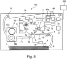
- FIG 8 is a schematic sectional view of an image forming apparatus 103 of this embodiment.
- the image forming apparatus 103 includes a cleaning device 31 as a cleaning means for removing a deposited matter, such as the toner residual toner or paper powder, remaining on the photosensitive drum 1 after passing through the transfer position Pe, from the surface of the photosensitive drum 1.
- the cleaning device 31 includes a cleaning blade 31a as a cleaning member provided so as to contact the surface of the photosensitive drum 1.
- a position where removal of the deposited matter on the photosensitive drum 1 by the cleaning blade 31a is performed is a cleaning position Ph.
- a charging brush 2 similar to the charging brush 2 in the embodiment 1 is provided so as to contact the photosensitive drum 1 in a first charging position Pi on the photosensitive drum 1 after passing through the cleaning position Ph (and before reaching the second charging position Pb). Except for the above-described point, a constitution and an operation of the image forming apparatus 103 of this embodiment are substantially the same as those of the image forming apparatus 100 of the embodiment 1.
- the image forming apparatus 103 includes the cleaning member 31a for removing the toner from the surface of the photosensitive drum 1 on a side downstream of the transfer position Pe and upstream of the first charging position Pi with respect to the rotational direction of the photosensitive member 1.
- the image forming apparatus 100 of the embodiment 1 had the cleaner-less constitution in which the transfer residual toner was collected and re-utilized by the developing device 5.
- the cleaning device 31 having a blade collection constitution such that the surface of the photosensitive drum 1 before reaching the charging brush 2 is cleaned is disposed. For that reason, in the image forming apparatus 103 of this embodiment, it is possible to suppress that the charging brush 2 is contaminated with the deposited matter, such as the transfer residual toner or the paper powder, with the increase in cumulative use amount of the charging brush 2.
- the lowering in first charging ratio R with the increase in cumulative use amount of the charging brush 2 is suppressed, so that the suppressing effect of the image defect due to the transfer memory can be more satisfactorily maintained.
- the first charging ratio R1 represented by the above-described formula (1) lowers in some cases.
- a potential difference of a predetermined value or more generates between the charging brush 2 and the photosensitive drum 1
- the electric discharge generates, and therefore, there is a limit in that the absolute value of the first charging voltage is made large.
- This embodiment aims at obtaining the suppressing effect of the image defect due to the transfer memory irrespective of the environment by suppressing the lowering in first charging ratio R1 with the low-temperature/low-humidity environment.
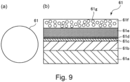
- a photosensitive drum 61 shown in parts (a) and (b) of Figure 9 is used instead of the photosensitive drum 1 in the image forming apparatus 100 of the embodiment 1. Except for this point, a constitution and an operation of the image forming apparatus of this embodiment are substantially the same as those of the image forming apparatus 100 of the embodiment 1.
- Part (a) of Figure 9 is a schematic sectional view of the photosensitive drum 61 in this embodiment
- part (b) of Figure 9 is a schematic sectional view showing a layer structure of the photosensitive drum 61 in this embodiment.
- the photosensitive drum 61 in this embodiment will be described.
- the photosensitive drum 61 in this embodiment has an electric charge injection function at an outermost surface.
- the photosensitive drum 61 includes an electroconductive supporting member 61a, an electroconductive layer 61b, an undercoat layer 61c, a photosensitive layer consisting of two layers of a charge generating layer 61d and a charge transporting layer 61e, and a charge injection layer 61f.
- the charge injection layer 61f forming the surface of the photosensitive drum 61 contains electroconductive particles 61g.
- the charge injection layer 61f is formed by dispersing the electroconductive particles 61g in a binder resin. A content of the electroconductive particles 61g is 5.0 vol.
- volume resistivity of the charge injection layer 61f is 1.0 ⁇ 10 9 ⁇ .cm or more and 1.0 ⁇ 10 14 ⁇ .cm or less.
- volume resistivity of the charge injection layer 61f is less than 1.0 ⁇ 10 9 ⁇ .cm, an electric resistance of the charge injection layer 61f is excessively low, and the electrostatic latent image cannot be appropriately formed, so that it becomes difficult to develop the electrostatic latent image into a predetermined image.
- the volume resistivity of the charge injection layer 61f exceeds 1.0 ⁇ 10 14 ⁇ .cm, the electric resistance of the charge injection layer 61f is excessively high, and a charge injection property of the electric charge from the charging brush 2 into the charge injection layer 61f lowers, and therefore, it becomes difficult to obtain, as an object of this embodiment, the first charging ratio R1 of not less than a predetermined value in the low-temperature/low-humidity environment.
- the content of the electroconductive particles 61g may desirably be 5.0 vol. % or more and 70.0 vol. % or less per the entire volume of the charge injection layer 61f.
- the volume resistivity of the charge injection layer 61f can be controlled by, for example, a particle size of the electroconductive particles 61g, other than the content of the electroconductive particles 61g.
- the particle size of the electroconductive particles 61g may preferably be 5 nm or more and 300 nm or less, more preferably be 40 nm or more and 250 nm or less in terms of a number-average particle size.
- the number-average particle size of the electroconductive particles 61g is less than 5 nm, a specific surface area of the electroconductive particles 61g becomes large, and a degree of water absorption in the neighborhood of the electroconductive particles 61g on the surface of the charge injection layer 61f becomes large, so that the volume-resistivity of the charge injection layer 61f is liable to lower.
- the number-average particle size of the electroconductive particles 61g exceeds 300 nm, not only a degree of dispersion of particle in the charge injection layer 61f becomes worse, but also an area of an interface with the binder resin lowers, so that a resistance in the interface increases and thus the charge injection property is liable to become worse.
- the electroconductive particles 61g contained in the charge injection layer 61f it is possible to cite particles of metal oxides such as titanium oxide, zinc oxide, tin oxide, indium oxide, and the like.
- the metal oxide may be doped with an element, such as niobium, phosphorus or aluminum, or an oxide thereof.
- the electroconductive particles 61g may have a lamination structure including core material particles and a coating layer coating the particles.
- the core material particles it is possible to cite particles of titanium oxide, barium sulfate, zinc oxide, and the like.
- the coating layer it is possible to cite layers of titanium oxide, tin oxide, and the like, and in this embodiment, the layer of titanium oxide is preferred from a viewpoint of the charge injection property from the charging brush 2.
- a content of the niobium may preferably be 0.5 wt. % or more and 15.0 wt. % or less, more preferably be 2.6 wt. % or more and 10.0 wt. % or less, per an entire weight of the niobium-containing titanium oxide particles.
- the titanium oxide particles containing the niobium may preferably be titanium oxide particles of an anatase type or a rutile type, and may more preferably be the titanium oxide particles of the anatase type.
- the titanium oxide particles are particles including the anatase type, titanium oxide particles as a core material and a coating layer of titanium oxide containing niobium at a surface of the core material.
- the anatase type titan oxide particles are used as the core material, and is coated with the niobium-containing titanium oxide at the surface thereof, so that the electric charge becomes easy to move in the charge injection layer 61f, and in addition, the charge injection property from the charging brush 2 into the charge injection layer 61f can be enhanced. Further, it is possible to suppress a lowering in volume resistivity of the charge injection layer 61f.
- the image forming apparatus 100 of this embodiment by using the photosensitive drum 61 including the charge injection layer 61f as the surface layer, even in a low-temperature/low-humidity environment, good charge injection can be performed between the charging brush 2 and the photosensitive drum 1.
- the image forming apparatus 100 of this embodiment it becomes possible to suppress the lowering in first charging ratio R1 in the low-temperature/low-humidity environment, so that it becomes possible to obtain the suppressing effect of the occurrence of the image defect due to the transfer memory irrespective of the environment.
- the present invention is not limited to such a constitution.
- an absolute value of the transfer voltage is made smaller in the sheet interval than during the sheet passing, when the surface potential of the photosensitive member in the position corresponding to the sheet interval is inverted in polarity to the opposite polarity to the normal charge polarity, the occurrence of the image defect due to the transfer memory can be suppressed by the present invention.
- the surface potential of the photosensitive member is inverted in polarity to the opposite polarity to the normal charge polarity, it is possible to suppress the occurrence of the image defect due to the transfer memory.
- the image is formed on a recording material is smaller in width of the photosensitive member in the rotational axis direction (widthwise direction substantially perpendicular to a recording material conveying direction) than a maximum image formable width in the image forming apparatus, a region of the photosensitive member directly contacting the transfer member in the transfer position can generate. In this region, the surface potential of the photosensitive member is inverted in polarity to the opposite polarity to the normal charge polarity similarly as the region corresponding to the sheet interval described in the above-described embodiments in some instances.
- the transfer memory in this region can be alleviated similarly as in the region corresponding to the sheet interval described in the above-described embodiments, so that the occurrence of the image defect due to the transfer memory in this region can be suppressed.
- the surface potential of the photosensitive member is capable of becoming a surface potential smaller in absolute value than the light-portion potential although the surface potential is not inverted in polarity to the opposite polarity to the normal charge polarity (see Figure 6 ).
- the surface potential in this region can also be uniformized in the first charging position, and therefore, it is advantageous in that the dark-portion potential is formed more uniformly in the second charging position.
- the photosensitive member is not limited to a drum-shaped image, but may also be a belt-shaped member or the like member.
- the transfer member is not limited to the roller-shaped member, but may also be a brush-shaped member, a sheet-shaped member, or the like member.
- an average interyarn distance of the charging brush may preferably be made smaller than (more preferably be made not more than 70 % of, further preferably be made not more than 50 % of) an average interyarn distance of the transfer brush.
- the charging brush as the first charging member was the brush member which was fixedly disposed, but for example, the charging brush may also be a brush roller constituted by including a core portion and a brush portion provided around the core portion.
- the image forming apparatus is not limited to the monochromatic image forming apparatus, but for example, the image forming apparatus may also be a color image forming apparatus including a plurality of image forming portions each including a photosensitive member and a process means actable on the photosensitive member. In this case, the present invention is applicable to at least one of the plurality of photosensitive members.
- the present invention even when the pre-exposure device is not provided, the transfer memory is alleviated, so that the occurrence of the image defect due to the transfer memory can be suppressed.
- the present invention is not limited thereto, but even in the case where the pre-exposure device is provided in the image forming apparatus, it is effective to alleviate the transfer memory by uniformizing the surface potential of the photosensitive member inverted in polarity to the opposite polarity to the normal charge polarity.
- each of the normal charge polarity of the photosensitive member and the normal charge polarity was the negative polarity, but may also be the positive polarity, and in that case, a person skilled in the art can appropriately change the polarity in such a manner that the polarity of each of various applied voltages is changed to the opposite polarity to the associated polarity in the above-described embodiments, or in the like manner.
Landscapes
- Physics & Mathematics (AREA)
- General Physics & Mathematics (AREA)
- Engineering & Computer Science (AREA)
- Plasma & Fusion (AREA)
- Microelectronics & Electronic Packaging (AREA)
- Electrostatic Charge, Transfer And Separation In Electrography (AREA)
- Discharging, Photosensitive Material Shape In Electrophotography (AREA)
Applications Claiming Priority (1)
| Application Number | Priority Date | Filing Date | Title |
|---|---|---|---|
| JP2023199524A JP2025085557A (ja) | 2023-11-26 | 2023-11-26 | 画像形成装置 |
Publications (1)
| Publication Number | Publication Date |
|---|---|
| EP4560403A1 true EP4560403A1 (fr) | 2025-05-28 |
Family
ID=93432157
Family Applications (1)
| Application Number | Title | Priority Date | Filing Date |
|---|---|---|---|
| EP24211067.4A Pending EP4560403A1 (fr) | 2023-11-26 | 2024-11-06 | Appareil de formation d'images |
Country Status (4)
| Country | Link |
|---|---|
| US (1) | US20250172896A1 (fr) |
| EP (1) | EP4560403A1 (fr) |
| JP (1) | JP2025085557A (fr) |
| CN (1) | CN120044769A (fr) |
Citations (3)
| Publication number | Priority date | Publication date | Assignee | Title |
|---|---|---|---|---|
| US8180256B2 (en) * | 2007-08-10 | 2012-05-15 | Canon Kabushiki Kaisha | Image forming apparatus featuring first and second brushes for charging residual toner |
| EP2515179A2 (fr) * | 2011-04-22 | 2012-10-24 | Canon Kabushiki Kaisha | Appareil de formation d'images |
| JP2016218155A (ja) | 2015-05-15 | 2016-12-22 | キヤノン株式会社 | 画像形成装置 |
Family Cites Families (1)
| Publication number | Priority date | Publication date | Assignee | Title |
|---|---|---|---|---|
| JP2003307909A (ja) * | 2002-04-17 | 2003-10-31 | Canon Inc | 帯電部材、該帯電部材を用いる帯電装置、及び画像記録装置 |
-
2023
- 2023-11-26 JP JP2023199524A patent/JP2025085557A/ja active Pending
-
2024
- 2024-11-06 EP EP24211067.4A patent/EP4560403A1/fr active Pending
- 2024-11-20 CN CN202411663575.1A patent/CN120044769A/zh active Pending
- 2024-11-25 US US18/958,975 patent/US20250172896A1/en active Pending
Patent Citations (3)
| Publication number | Priority date | Publication date | Assignee | Title |
|---|---|---|---|---|
| US8180256B2 (en) * | 2007-08-10 | 2012-05-15 | Canon Kabushiki Kaisha | Image forming apparatus featuring first and second brushes for charging residual toner |
| EP2515179A2 (fr) * | 2011-04-22 | 2012-10-24 | Canon Kabushiki Kaisha | Appareil de formation d'images |
| JP2016218155A (ja) | 2015-05-15 | 2016-12-22 | キヤノン株式会社 | 画像形成装置 |
Also Published As
| Publication number | Publication date |
|---|---|
| JP2025085557A (ja) | 2025-06-05 |
| CN120044769A (zh) | 2025-05-27 |
| US20250172896A1 (en) | 2025-05-29 |
Similar Documents
| Publication | Publication Date | Title |
|---|---|---|
| US9665032B2 (en) | Image forming apparatus with exposure controlled in dependence on cumulative operating time and humidity | |
| JP2004117960A (ja) | 画像形成装置 | |
| US7756446B2 (en) | Image forming apparatus | |
| US7805089B2 (en) | Image forming apparatus | |
| US20230048499A1 (en) | Image forming apparatus | |
| JP2004069860A (ja) | 画像形成装置 | |
| US6915088B2 (en) | Image forming apparatus | |
| JP4314719B2 (ja) | 画像形成装置及びプロセスカートリッジ | |
| EP4560403A1 (fr) | Appareil de formation d'images | |
| US11852986B2 (en) | Image forming apparatus | |
| US20250341802A1 (en) | Image forming apparatus | |
| US20060165438A1 (en) | Image forming apparatus | |
| US20260010092A1 (en) | Image forming apparatus | |
| US12298687B2 (en) | Image forming apparatus with control of transfer voltage | |
| JP7225361B1 (ja) | 画像形成装置 | |
| US20240019795A1 (en) | Image forming apparatus | |
| US6741824B2 (en) | Charging system, process cartridge and image forming apparatus | |
| JP2005165114A (ja) | 画像形成装置 | |
| JPH086282A (ja) | 画像形成装置 | |
| JP2002014522A (ja) | 画像記録装置 | |
| JP2004077971A (ja) | 画像形成装置 | |
| JP2002040825A (ja) | 画像形成装置 | |
| JP2001343811A (ja) | 画像形成装置 | |
| JP2001343866A (ja) | 画像形成装置 | |
| JP2003233243A (ja) | 画像形成装置 |
Legal Events
| Date | Code | Title | Description |
|---|---|---|---|
| PUAI | Public reference made under article 153(3) epc to a published international application that has entered the european phase |
Free format text: ORIGINAL CODE: 0009012 |
|
| STAA | Information on the status of an ep patent application or granted ep patent |
Free format text: STATUS: THE APPLICATION HAS BEEN PUBLISHED |
|
| AK | Designated contracting states |
Kind code of ref document: A1 Designated state(s): AL AT BE BG CH CY CZ DE DK EE ES FI FR GB GR HR HU IE IS IT LI LT LU LV MC ME MK MT NL NO PL PT RO RS SE SI SK SM TR |
|
| STAA | Information on the status of an ep patent application or granted ep patent |
Free format text: STATUS: REQUEST FOR EXAMINATION WAS MADE |
|
| 17P | Request for examination filed |
Effective date: 20251128 |