EP4560654A2 - Elektronisches bauelement zur einschaltstrombegrenzung und verwendung eines elektronischen bauelements - Google Patents
Elektronisches bauelement zur einschaltstrombegrenzung und verwendung eines elektronischen bauelements Download PDFInfo
- Publication number
- EP4560654A2 EP4560654A2 EP25169735.5A EP25169735A EP4560654A2 EP 4560654 A2 EP4560654 A2 EP 4560654A2 EP 25169735 A EP25169735 A EP 25169735A EP 4560654 A2 EP4560654 A2 EP 4560654A2
- Authority
- EP
- European Patent Office
- Prior art keywords
- ntc
- electronic component
- elements
- contact
- ntc element
- Prior art date
- Legal status (The legal status is an assumption and is not a legal conclusion. Google has not performed a legal analysis and makes no representation as to the accuracy of the status listed.)
- Pending
Links
Images


Classifications
-
- H—ELECTRICITY
- H01—ELECTRIC ELEMENTS
- H01C—RESISTORS
- H01C1/00—Details
- H01C1/14—Terminals or tapping points specially adapted for resistors; Arrangements of terminals or tapping points on resistors
- H01C1/1413—Terminals or electrodes formed on resistive elements having negative temperature coefficient
-
- H—ELECTRICITY
- H01—ELECTRIC ELEMENTS
- H01C—RESISTORS
- H01C17/00—Apparatus or processes specially adapted for manufacturing resistors
- H01C17/28—Apparatus or processes specially adapted for manufacturing resistors adapted for applying terminals
- H01C17/281—Apparatus or processes specially adapted for manufacturing resistors adapted for applying terminals by thick film techniques
-
- H—ELECTRICITY
- H01—ELECTRIC ELEMENTS
- H01C—RESISTORS
- H01C7/00—Non-adjustable resistors formed as one or more layers or coatings; Non-adjustable resistors made from powdered conducting material or powdered semi-conducting material with or without insulating material
- H01C7/001—Mass resistors
-
- H—ELECTRICITY
- H01—ELECTRIC ELEMENTS
- H01C—RESISTORS
- H01C7/00—Non-adjustable resistors formed as one or more layers or coatings; Non-adjustable resistors made from powdered conducting material or powdered semi-conducting material with or without insulating material
- H01C7/04—Non-adjustable resistors formed as one or more layers or coatings; Non-adjustable resistors made from powdered conducting material or powdered semi-conducting material with or without insulating material having negative temperature coefficient
- H01C7/041—Non-adjustable resistors formed as one or more layers or coatings; Non-adjustable resistors made from powdered conducting material or powdered semi-conducting material with or without insulating material having negative temperature coefficient formed with two or more layers
-
- H—ELECTRICITY
- H01—ELECTRIC ELEMENTS
- H01C—RESISTORS
- H01C7/00—Non-adjustable resistors formed as one or more layers or coatings; Non-adjustable resistors made from powdered conducting material or powdered semi-conducting material with or without insulating material
- H01C7/04—Non-adjustable resistors formed as one or more layers or coatings; Non-adjustable resistors made from powdered conducting material or powdered semi-conducting material with or without insulating material having negative temperature coefficient
- H01C7/042—Non-adjustable resistors formed as one or more layers or coatings; Non-adjustable resistors made from powdered conducting material or powdered semi-conducting material with or without insulating material having negative temperature coefficient mainly consisting of inorganic non-metallic substances
- H01C7/043—Oxides or oxidic compounds
-
- H—ELECTRICITY
- H01—ELECTRIC ELEMENTS
- H01C—RESISTORS
- H01C7/00—Non-adjustable resistors formed as one or more layers or coatings; Non-adjustable resistors made from powdered conducting material or powdered semi-conducting material with or without insulating material
- H01C7/06—Non-adjustable resistors formed as one or more layers or coatings; Non-adjustable resistors made from powdered conducting material or powdered semi-conducting material with or without insulating material including means to minimise changes in resistance with changes in temperature
-
- H—ELECTRICITY
- H01—ELECTRIC ELEMENTS
- H01C—RESISTORS
- H01C7/00—Non-adjustable resistors formed as one or more layers or coatings; Non-adjustable resistors made from powdered conducting material or powdered semi-conducting material with or without insulating material
- H01C7/18—Non-adjustable resistors formed as one or more layers or coatings; Non-adjustable resistors made from powdered conducting material or powdered semi-conducting material with or without insulating material comprising a plurality of layers stacked between terminals
Definitions
- the invention relates to an electronic component for limiting inrush current.
- the invention further relates to the use of an electronic component.
- a thermally controlled inrush current limiter can be used for starting an internal combustion engine.
- ICL thermally controlled inrush current limiter
- the starter motor's current draw briefly places a load of up to 1000 A on the 12 V vehicle electrical system. This additional power places such a heavy load on conventional 12 V batteries that the mains voltage drops by several volts. This drop can lead to the failure of other consumers in the vehicle electrical system. To avoid this, the voltage drop must be avoided or reduced.
- An NTC (Negative Temperature Coefficient) component for example, can be used to reduce the voltage drop.
- the NTC component With the expected dimensions of more than 1 cm 2 cross-section and less than 1 mm length of the NTC component, a surface contact with a low electrical Resistance is required. Furthermore, the component is exposed to significant temperature fluctuations during operation, with the thermal expansion coefficient of the ICL ceramic being significantly lower than that of good electrical conductors (e.g., copper). The resulting thermal mechanical stresses can lead to component destruction.
- good electrical conductors e.g., copper
- One problem to be solved is to provide an improved electronic component for inrush current limitation and the use of an improved electronic component.
- an electronic component or component for short, is specified.
- the electronic component is designed to be used in an inrush current limiter or to act as an inrush current limiter.
- the component has at least one NTC element.
- the NTC element serves as a functional element or functional layer of the component.
- the NTC element has an NTC ceramic.
- the component can have a plurality of NTC elements, for example two, three, five, or ten NTC elements.
- the NTC element can be disk- or plate-shaped (round). However, the NTC element can also have a rectangular or annular surface.
- a metallization is arranged on the NTC element, preferably on a top side and a bottom side of the NTC element.
- the metallization preferably comprises silver.
- the metallization can also be copper or gold.
- the NTC element can be a monolithic component.
- the NTC ceramic is manufactured using compression molding technology and then lapped (finely ground on both sides) to the desired shape or thickness (thick-film monolith).
- the NTC element can also be designed as a multilayer monolith. In this case, ceramic foils are stacked on top of each other and pressed together to create the NTC element.
- the component has at least two electrically conductive contact elements or electrodes.
- the contact elements are flat.
- the contact elements are designed and arranged for electrically conductive and thermal connection with the NTC element.
- the component can have a plurality of contact elements, for example, five, ten, or 15 contact elements, whereby the individual NTC elements must be well thermally coupled.
- the NTC element is electrically connected to the respective contact element via a connecting material.
- the NTC element is also thermally connected to the respective contact element via the connecting material.
- the connecting material creates a stable, highly electrically conductive, and mechanically durable connection between the NTC element and the contact elements.
- the thermal expansion coefficient of the respective contact element is adapted to the thermal expansion coefficient of the NTC element.
- the thermal expansion coefficients of the NTC element and the contact elements are approximately the same.
- the NTC element has a thermal expansion coefficient between 7 ppm/K and 10 ppm/K.
- the respective contact element has a corresponding expansion coefficient.
- the thermal expansion coefficient of the respective contact element is preferably in the range between 5 ppm/K and 10 ppm/K.
- CTE material-induced thermal expansion
- the NTC element has a top side and a bottom side.
- the top side and bottom side are opposite each other and are each bounded by the end faces of the NTC element.
- the top side and bottom side are each at least partially electrically contacted by the respective contact element.
- a small edge layer or a small edge area of the top side or bottom side may remain uncontacted.
- the top and bottom sides can also be electrically connected over their entire surface by the respective contact element.
- the NTC element is embedded between the two contact elements, so that the top and bottom sides are each partially or completely covered by a contact element. This allows for particularly reliable contacting of the NTC element. and a particularly stable connection between the NTC element and the contact elements can be achieved.
- the contact element comprises a material composite.
- the contact element is composed of several materials.
- the respective contact element preferably comprises copper. Copper is characterized by its very high electrical conductivity and very high thermal conductivity.
- the contact element preferably comprises Invar and/or Kovar and/or molybdenum. These materials are characterized by their low thermal expansion coefficients.
- the respective contact element comprises a rolled copper-Invar sheet with a layer structure of copper-Invar-copper.
- the contact element has a layer structure of copper - Invar - copper with a thickness ratio of 10% ⁇ copper ⁇ 30% - 50% ⁇ Invar / Kovar / Molybdenum ⁇ 80% - 10% ⁇ copper ⁇ 30%.
- a first layer preferably comprises copper.
- the first layer has a thickness or vertical extent that is between 1/10 and 3/10 of the total thickness of the contact element.
- a second layer preferably comprises Kovar and/or Invar and/or molybdenum.
- the second layer has a thickness that is between 5/10 and 8/10 of the total thickness of the contact element.
- the third layer has a thickness between 1/10 and 3/10 of the total thickness of the contact element.
- the layer of the contact element containing Invar/Kovar/molybdenum is thicker than the layer containing copper. This allows the contact element's coefficient of expansion to be reduced or adapted to the coefficient of expansion of the NTC element.
- the preferred thickness ratio of copper to Invar to copper is 20% - 60% - 20%.
- Other thickness ratios and layer sequences and numbers of layers, as well as the addition of Kovar or molybdenum, are also conceivable to achieve the desired coefficient of expansion.
- the connecting material comprises sintered silver.
- Sintered silver exhibits high electrical and thermal conductivity. Furthermore, sintered silver can withstand high temperatures of up to 400°C, for example, 300°C, as well as rapid and frequent temperature changes.
- the hot state refers to a state at a temperature that is higher than that of the NTC element in its ground state.
- the temperature range between the ground state and the hot state can, for example, span any temperature range between -55°C and +300°C or extend beyond this range.
- the Temperature range between the ground state and the hot state extends over the range from -40°C to +300°C.
- the bonding material preferably comprises ⁇ Ag.
- ⁇ Ag is particularly characterized by its sufficient porosity.
- the NTC element has two, three, five, ten, or more segments.
- the segments of the NTC element preferably represent rectangular subregions of the NTC element that are spaced apart from one another.
- the distance between the segments is 0.05 mm to 0.2 mm, for example, 0.1 mm.
- the NTC element has a nominal resistance R 25 ⁇ 1 ⁇ at a temperature of 25°C (room temperature).
- Room temperature is understood to be the temperature typically prevailing in occupied rooms.
- the electrical resistance preferably describes the electrical resistance of the unloaded NTC element between external contacts at an ambient temperature of 25°C.
- the NTC element has a nominal resistance R 25 of less than or equal to 0.1 ⁇ , preferably less than 0.05 ⁇ , at the specified temperature.
- the NTC element therefore has a very low electrical resistance at room temperature or at 25°C and thus a very high electrical conductivity. This makes the NTC element particularly suitable for use in an inrush current limiter with a high current load.
- the low electrical resistance makes it possible, in particular, to ensure that a sufficiently high inrush current is provided to an electrical load, which is connected in series with the electronic component in a corresponding application, for example, but is limited to such an extent that, for example, the electrical voltage during the switch-on process is still sufficiently high to supply electrical power to other important electrical components.
- the voltage drop during the load's start-up process is reduced by approximately 1 V compared to a load without the electronic component.
- the specific electrical resistance of the NTC element in a ground state of the electronic component is ⁇ 2 ⁇ cm.
- the specific electrical resistance of the NTC element in a ground state of the electronic component is between 0.1 ⁇ cm and 1.0 ⁇ cm, for example, 0.3 ⁇ cm.
- the contact element has a thickness d.
- 0.3 mm ⁇ d ⁇ 0.8 mm applies.
- the thickness d of the respective contact element is less than 0.7 mm, for example, 0.6 mm.
- the component comprises a plurality of NTC elements and contact elements.
- the plurality of NTC elements can be provided by singulation from a substrate.
- the NTC elements are connected in parallel.
- the current carrying capacity The component's thermal conductivity and/or current-carrying capacity can be increased by connecting multiple NTC elements in parallel.
- the NTC elements are preferably stacked one above the other.
- a contact element is arranged between each two adjacent NTC elements.
- the NTC elements are thermally well coupled to one another via the contact elements.
- the NTC element has the composition La (1-x) EA (x) Mn (1-abc) Fe (a) Co (b) Ni (c) O (3 ⁇ ) .
- EA denotes an alkaline earth element.
- the alkaline earth element is preferably selected from magnesium, calcium, strontium, or barium.
- ⁇ denotes the deviation from the stoichiometric oxygen ratio (oxygen excess or oxygen deficit).
- 0.
- This composition provides an NTC element characterized by exceptionally high electrical conductivity and a sufficient B value (thermistor constant).
- the resistance can be further varied and controlled by (a) specific thickness and (a) specific cross-section or area of the NTC element.
- the NTC element has a thickness d. Preferably, 100 ⁇ m ⁇ d ⁇ 600 ⁇ m applies.
- the thickness d of the NTC element is preferably less than 500 ⁇ m, for example 400 ⁇ m.
- the B value B 25/100 is in the range between 1000 K and 4000 K, preferably between 1400 K and 2000 K, for example 1500 K.
- the component has a fastening element.
- the fastening element is Preferably designed and arranged to establish an electrically conductive connection with battery lines.
- the fastening element is further preferably designed and arranged to establish a mechanical connection with battery lines.
- the fastening element is further preferably designed and arranged to provide an indirect mechanical connection between the contact elements.
- the fastening element can be designed to form a screw connection. However, the fastening element can also be designed, for example, to form a clamp connection.
- the fastening element can further comprise a sealing element.
- the sealing element can be insulating or partially insulating.
- the fastening element can comprise at least one nut and one screw and/or at least one clamping element, for example, two clamping elements.
- the fastener exhibits an electrical resistance. This electrical resistance is equal to or only slightly higher than the resistance of the NTC element at low operating temperatures. In particular, the electrical resistance of the fastener is equal to or only slightly higher than the resistance of the NTC element at the lowest operating temperature, e.g., -40°C.
- an electronic component is described.
- the use of the component described above is specified. All features explained in connection with the component also apply to the use, and vice versa.
- the temperature-dependent resistor limits the inrush current during switch-on.
- the NTC element Upon switch-on, the NTC element immediately heats up due to the inrush current (e.g., to 250°C), causing the NTC resistance to quickly decrease to a very small residual resistance (e.g., 0.5 m ⁇ ). Due to the specific properties of the NTC element, this dynamic resistance change reduces the current peak caused by the starter motor, which simultaneously reduces the voltage drop in the battery. This provides an effective component for limiting inrush current in start/stop systems.
- the provided contact elements and the connecting material also provide a very low-resistance electrical connection between the NTC element and the contact elements for repeated switching cycles, where the ambient temperature can fluctuate from -40°C to 120°C. During the switching cycle, the temperature can reach up to 300°C. This results in a stable, highly electrically conductive component with a mechanically durable, temperature-resistant, and extremely resilient connection between the NTC element and contact elements for use in start/stop systems in the automotive sector.
- an electronic component in particular the electronic component described above, for currents up to 1000 A at direct voltage in 12 V and 24 V networks is specified.
- the Figure 1 shows an electronic component 1, or component 1 for short.
- Component 1 is designed to be used as an inrush current limiter or in an inrush current limiter for start/stop systems in 12 V and 24 V networks in the automotive sector.
- Component 1 is particularly suitable for use with currents up to 1000 A (at direct voltage in 12 V and 24 V networks).
- Component 1 is suitable for use in typical 12 V starter motors with approximately 1 kW to 3 kW of power.
- Component 1 comprises an NTC element 2 or an NTC ceramic.
- NTC element 2 represents a functional layer or a functional element of component 1.
- NTC element 2 is a thermally conductive component with a negative temperature coefficient.
- the NTC element 2 has a material composition which is characterized by high electrical conductivity and low specific resistance.
- the NTC element 2 preferably has the following composition: La (1-x) EA (x) Mn (1-abc) Fe (a) Co (b) Ni (c) O (3 ⁇ ) .
- EA stands for an alkaline earth element, for example Mg, Ca, Sr or Ba.
- ⁇ denotes the deviation from the stoichiometric oxygen ratio (oxygen excess or oxygen deficit).
- 0.
- the NTC ceramic has the composition La 0.95 Sr 0.05 MnO 3 .
- the specific electrical resistance of the NTC element 2 in a ground state of the NTC element 2 is less than or equal to 2 ⁇ cm, preferably ⁇ 1 ⁇ cm, for example, 0.5 ⁇ cm.
- the ground state describes a temperature of the NTC element 2 of 25°C or at room temperature.
- the ground state can be an unloaded state in which, for example, no electrical power is applied to the NTC element 2.
- the NTC element 2 has an electrical resistance (nominal resistance R 25 ) of less than or equal to 1 ⁇ , preferably less than 0.1 ⁇ , for example, 0.05 ⁇ .
- the NTC element 2 therefore has a low electrical resistance at room temperature or at 25°C and thus a high electrical conductivity. This makes the NTC element 2 particularly suitable for use in an inrush current limiter.
- the NTC element 2 also has a high B value.
- the B value B 25/100 is in the range between 1000 K and 4000 K, preferably between 1400 K and 2000 K, for example 1500 K.
- the NTC element 2 has a low thermal expansion coefficient. Typically, the thermal Expansion coefficient of NTC element 2 between 7 ppm/K and 10 ppm/K.
- the NTC element 2 is preferably designed as a monolithic component.
- the NTC element 2 is a thick-film monolith.
- the NTC element 2 is manufactured using compression molding technology and then lapped (finely ground on both sides) to the desired thickness.
- the NTC element 2 can also be designed as a multilayer monolith. In this case, ceramic foils are stacked on top of each other and pressed to create the NTC element 2.
- the NTC element 2 shown has a round shape.
- the NTC element 2 is disc-shaped or plate-shaped. However, other shapes are also conceivable for the NTC element 2, for example a rectangular shape or a ring shape.
- the NTC element 2 can be in the form of a substrate.
- the NTC element 2 has an area between 25 mm 2 and 500 mm 2 , for example 200 mm 2.
- the diameter of the NTC element 2 is, for example, less than or equal to 14 mm, e.g. 13.75 mm.
- the NTC element 2 has a thickness d between 100 ⁇ m and 600 ⁇ m, for example 400 ⁇ m. By varying the thickness d and/or cross-section or area of the NTC element 2, the resistance of the NTC element 2 can be varied and controlled.
- the NTC element 2 has a metallization (not explicitly shown).
- the metallization is preferably arranged on a top side and a bottom side of the NTC element 2.
- the metallization preferably comprises baked-on silver.
- the component 1 further comprises two contacts 3 or contact elements 3 (plus contact and minus contact element 12b, 12a, see Figure 3 ).
- the contact elements 3 serve to make electrical contact with the NTC element 2.
- the contact elements 3 lie fully on the top and bottom of the NTC element 2.
- a narrow edge area of the top and bottom can also remain free of the respective contact element 3.
- the contact elements 3 are each electrically connected to the top and bottom of the NTC element 2.
- the NTC element 2 and the contact elements 3 are sintered.
- the component 1 comprises a connecting material 7.
- a layer of connecting material 7 is formed between the top side of the NTC element 2 and the first contact element 3, as well as between the bottom side of the NTC element 2 and the second contact element 7.
- the layer thickness of the connecting material 7 is preferably in the range between 15 ⁇ m and 80 ⁇ m, for example, 20 ⁇ m.
- the connecting material 7 is characterized by high electrical and thermal conductivity.
- the connecting material 7 is further preferably characterized by high porosity.
- the connecting material 7 is further characterized by its ability to withstand high temperatures of up to 400°C, e.g., 300°C, as well as the numerous and rapid temperature changes that can occur during operation or when the component 1 is hot.
- the hot state refers to a state of the component 1 at a temperature that is greater than that of the component 1 in the ground state.
- the temperature range between the ground state and the hot state can, for example, span any temperature range between -55°C and +300°C or extend beyond this range.
- the temperature range between the ground state and the hot state can extend beyond the range from -40°C to +300°C.
- the connecting material 7 comprises sintered silver Ag or ⁇ Ag.
- Sintered silver has the advantage of having sufficient porosity.
- the connecting material 7 creates a stable, highly electrically conductive, and mechanically durable connection between the NTC element 2 and the contact elements 3.
- the respective contact element 3 has high thermal and electrical conductivity.
- the respective contact element 3 is further configured to reduce thermal stresses between the NTC element 2 and the contact element 3.
- the respective contact element 3 is configured to reduce or minimize differences in material-related thermal expansion (CTE).
- the respective contact element 3 comprises a composite material.
- the respective contact element can be formed, for example, as a composite sheet.
- the composite material can comprise copper-Invar-copper (CIC).
- CIC copper-Invar-copper
- Kovar or molybdenum can also be used as the material.
- Invar, Kovar, or molybdenum has a low thermal expansion coefficient.
- the thermal expansion coefficient of these materials is ⁇ 10 ppm / K, for example 7 ppm / K. This means that the expansion coefficient of Kovar / Invar / Molybdenum is very similar to the expansion coefficient of the NTC element 2.
- the expansion coefficient of the contact element 3 can be well adapted to the expansion coefficient of the NTC element 2. Thermal stresses can be reduced or avoided.
- the respective contact element 3 is a rolled copper-Invar sheet with a layer structure of copper-Invar-copper of 20%-60%-20%.
- a layer structure of copper-Invar-copper 20%-60%-20%.
- other ratios of copper to Invar or Kovar to molybdenum are also conceivable.
- other layer sequences and layer thicknesses can also be used.
- the contact elements 3 enclose the NTC element 2 in a pincer-like manner.
- a first partial region 3a of the respective contact element 3 rests on the top or bottom of the NTC element 2 and runs parallel to the top or bottom of the NTC element 2 or to a longitudinal axis L of the component 1.
- a length or horizontal extent of the NTC element 2 is preferably less than or equal to the length or horizontal extent of the first partial region 3a.
- a second partial region 3b of the respective contact element 3 encloses an angle with the longitudinal axis L.
- the second partial region 3b preferably adjoins the first partial region 3a at an angle of ⁇ 20°, for example 15°, to the longitudinal axis L of the component 1.
- the angle between the The angle between the second partial region 3b of the first contact element 3 and the second partial region 3b of the second contact element is preferably less than or equal to 40°, for example 30°.
- a third partial region 3c of the respective contact element 3 adjoins the second partial region 3b and runs parallel to the longitudinal axis L.
- the respective subregions 3a, 3b, 3c preferably have the same length.
- the subregions 3a, 3b, 3c each have a length of 10 mm to 15 mm.
- the respective subregions 3a, 3b, 3c preferably have the same thickness d.
- the sub-areas 3a, 3b, and 3c merge into one another.
- the sub-areas 3a, 3b, and 3c are not designed as separate areas or components, but rather represent subsections of the respective contact element 3.
- the respective contact element 3, in particular the third partial area 3c, has a recess 8.
- the third partial area 3c has a larger horizontal extent or a larger area than the first and second partial areas 3a, 3b (see, for example, Figure 3 ).
- the recess 8 is preferably circular.
- the recess 8 has, for example, a diameter of 8 mm.
- the recess 8 completely penetrates the contact element 3.
- the recess 8 serves to fix the component 1 by means of a fastening element with To connect battery cables, such as in connection with Figure 2 is explained in more detail.
- the Figure 2 shows a possible contacting of the component 1 according to the Figure 1 with the battery cables via cable lugs.
- the component 1 has a fastening element for establishing electrical contact with the component 1 and, in particular, for mechanically fastening battery leads to the component 1.
- the fastening element can be designed to provide a screw connection as described below. Alternatively, the fastening element can also be designed and arranged to establish a clamp connection.
- a spacer 9 is arranged between the first and second contact elements 3.
- the spacer 9 is arranged between a bottom side of the third partial area 3c of the first or upper contact element 3 and the top side of the third partial area 3c of the second or lower contact element 3.
- the spacer 9 is cylindrical.
- the spacer 9 is designed to be insulating.
- the spacer 9 serves to provide electrical insulation between the two contact elements 3 (positive contact element 12b and negative contact element 12a, see Figure 3 ).
- the spacer 9 comprises, for example, polytetrafluoroethylene (PTFE).
- PTFE polytetrafluoroethylene
- PTFE has the advantage that it is consistently insulating up to a temperature of approximately 250° C.
- the spacer 9 has a recess (not explicitly shown), which completely penetrates the spacer 9 in the vertical direction.
- the recess serves to accommodate a connecting element, e.g., a threaded rod 11, for example, a screw.
- a nut 10 is arranged on the top side of the first contact element 3 and the bottom side of the second contact element 3, respectively. Threaded rod 11 and nuts 10 serve to screw the contact elements 3 and to electrically and mechanically connect the component 1 to the battery lines (not explicitly shown).
- clamping elements for example, can be provided for clamping the contact elements 3 and/or for electrically and mechanically connecting the component 1 to the battery lines (not explicitly shown).
- Cable lugs 5 to which a copper cable (not shown) is attached, are arranged between the battery cables (not shown) and the contact elements 3.
- the cable lugs 5 are electrically connected to the contact elements 3.
- the threaded rod 11 is guided through the nuts 10, the recess 8 in the respective contact element 3, and the recess in the spacer 9.
- the screw connection on an axis avoids additional mechanical stress on the connection between the NTC element 2 and the contact elements 3.
- the screw connection or fastening must either have a higher resistance than the NTC element 2 or must be designed to be insulating (see for example Figures 12 and 13 ).
- the screw connection Alternatively, the connection or attachment can also be made directly to a ground contact on the vehicle or the starter motor.
- the temperature-dependent resistance of component 1 limits the inrush current during power-on.
- NTC element 2 Upon power-on, NTC element 2 immediately heats up due to the inrush current (e.g., to 250°C), causing the NTC resistance to rapidly decrease to a very small residual resistance (e.g., 0.5 m ⁇ ).
- This dynamic resistance change reduces the current peak caused by the starter motor, which simultaneously reduces the voltage drop in the battery. This provides a stable, durable, and efficient component for inrush current limitation.
- Component 1 can also be equipped with a so-called "fail-safe" function.
- the Figure 2 The screw connection shown is designed so that its electrical resistance is equal to or only slightly higher than the resistance of NTC element 2 at the lowest operating temperature, e.g., -40°C.
- the resistance of this screw connection is not temperature-dependent. This means that even in the event of a fault (e.g., a break in the conductive connection between NTC element 2 and contact element 3), the engine can still be started (depending on the design of the starter system).
- the voltage drop is also avoided, but the electrical power available for starting is severely limited, which may significantly delay the starting process.
- R spec,25 0.2 ⁇ cm.
- a fixed resistor or another conductive element with a defined electrical resistance can be used.
- the Figure 3 shows a perspective view of an electronic component according to a further embodiment.
- Component 1 has according to Figure 3 several NTC elements 2 and several contact elements 3.
- the component 1 can have up to ten NTC elements 2.
- the NTC elements 2 are each round or disc-shaped (see explanations on Figure 1 ).
- the NTC elements 2 are electrically connected in parallel.
- Contact elements 3 are arranged between NTC elements 2.
- Component 1 preferably has a layer sequence of alternating NTC elements 2 and contact elements 3 (positive contact elements 12b and negative contact elements 12a).
- the flat, "stacked" sequence of contact element 3 / NTC element 2 / contact element 3 / NTC element 2, etc., achieves a good thermal connection between the individual NTC elements 2. This good thermal connection enables uniform heating of NTC elements 2.
- the diameter of the NTC elements 2 can be smaller than the diameter of the Figure 1 NTC element 2 shown. This means that several smaller elements are connected. The stresses decrease with the component size of NTC element 2.
- the fastening to, preferably the screw connection to, the battery terminals is preferably carried out on a common insulating body (for example a spacer 9) in order to avoid additional mechanical stresses on the connection between the NTC elements 2 and the contact elements 3.
- a common insulating body for example a spacer 9
- component 1 according to the Figure 3 , in particular the material, structure and functioning of NTC elements 2 and contact elements 3 as well as their connection via the connecting material 7 and the functioning of the component 1 correspond to the Figure 1 described characteristics.
- the Figure 4 shows a schematic sectional view of an electronic component according to a further embodiment.
- the contact elements 3 are double-sided.
- the respective contact element 3 has three sub-areas 3a, 3b, 3c, where second sub-area 3b and third sub-area 3c are similar but in the opposite direction to the first sub-area 3a.
- the first partial region 3a rests on the top or bottom of the NTC element 2 and runs parallel to the top or bottom of the NTC element 2 or to the longitudinal axis L.
- the length or horizontal extent of the NTC element 2 is less than or equal to the length or horizontal extent of the first partial region 3a.
- the length of the first partial region 3a in this embodiment is greater than the length of the first partial region 3a according to the Figure 1 shown embodiment.
- the length of the first partial region 3a is, for example, 18 mm.
- the diameter of the NTC element 2 is, for example, less than or equal to 14 mm, e.g., 13.75 mm.
- the second and third subregions 3b, 3c each adjoin a side region or edge region of the first subregion 3a.
- the second subregion 3b and the third subregion 3c are formed to the left and right of the first subregion 3a, respectively.
- the second sub-region 3b and the third sub-region 3c each enclose an angle with the longitudinal axis L.
- the second and third sub-regions 3b, 3c preferably each enclose an angle of ⁇ 90°, for example 60°, with the longitudinal axis L.
- Both the second sub-region 3a and the third sub-region 3c extend away from the longitudinal axis L.
- a vertical distance from an end region 13 of the third sub-region 3c or the second sub-region 3b to the NTC element 2 is less than or equal to 18 mm, for example 15 mm.
- the component 1 is designed to be mirror-symmetrical about the axis L.
- the respective contact element 3 is also designed to be mirror-symmetrical about a vertical axis V.
- the design described above allows, for example, the electrical and thermal resistance of the contact elements 3 to be halved while using the same contact material.
- a further advantage of this design is the avoidance of different temperatures in the NTC element 2 by "one-sided" heat dissipation via the contact elements 3, as in the design according to Figure 1 .
- the Figure 5 shows a perspective view of a possible contacting of the electronic component according to Figure 4 .
- the component 1 is placed in a housing 6.
- the housing 6 is frame-shaped.
- the component 1 is contacted (screwed, clamped, or similar) through the housing 6 by means of an insulated, flexible copper cable (not explicitly shown).
- the contacting is carried out as in connection with the Figure 2 described via the nuts 10, the threaded rod 11, which is inserted into the recess 8 of the respective contact element 3, as well as the electrically conductive connection of the contact elements 3 with cable lugs, in which the copper cables
- the copper cables are introduced into the housing 6 via recesses 6a on a top and bottom side of the housing 6.
- the housing 6 has a mechanical strain relief 4 for the copper cables.
- the strain relief 4 can be arranged, for example, on a top side and a bottom side 4 of the housing 6. When mechanical tension is applied to the copper cables, the strain relief 4 ensures that no or only minimal forces act on the component 1 and, in particular, the connecting material 7. The component 1 is therefore preferably held stress-free by the strain relief 4.
- the Figure 6 shows a schematic sectional view of an electronic component according to a further embodiment.
- component 1 corresponds to component 1 from Figure 4
- the contact elements 3 are not arranged mirror-symmetrically to the longitudinal axis L. Rather, the contact elements 3 are offset from each other by 90°. This allows for different installation situations to be accommodated.
- the Figure 7 shows a perspective view of an electronic component according to a further embodiment.
- component 1 corresponds to component 1 from Figure 6
- the component 1 according to Figure 7 several NTC elements 2 and several contact elements 3.
- the component 1 can have up to ten NTC elements 2, each of which is round or disc-shaped and electrically connected in parallel.
- the contact elements 3 are arranged between the NTC elements 2.
- the component 1 thus has, as already described in connection with the Figure 3 described a layer sequence of alternatingly arranged NTC elements 2 and contact elements 3.
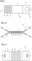
- FIG 8 shows a schematic sectional view of an electronic component according to a further embodiment.
- Figure 9 further shows a plan view of a portion of the electronic component according to Figure 8 .
- NTC element 2 In contrast to the embodiment according to the Figure 1 An NTC element 2 is used, which has been divided or segmented into smaller NTC elements or segments 2a by sawing or scoring.
- the NTC element 2 has a plurality of segments 2a.
- the NTC element 2 has, unlike in Figure 1 preferably a rectangular shape.
- the NTC element 2 has a width and a height of less than or equal to 13 mm, for example 12.7 mm.
- the respective segment 2a is also preferably rectangular.
- the respective segment 2a has a length and a width of approximately 2 mm each.
- the contact elements 3 should also be rectangular for this design.
- the respective contact element is Figures 8 and 9 formed from three rectangular sub-areas 3a, 3b, 3c.
- the three sub-areas preferably have the same length, for example 15 mm.
- the expansion joints 15 have a width of 0.05 mm to 0.2 mm, for example, 0.1 mm. These expansion joints 15 reduce thermal stresses in the NTC element 2 during normal operation.
- ceramic multilayer technology is suitable, in which an NTC substrate made of stacked ceramic foils is segmented by so-called "dicing" before or after metallization. All other features correspond to those associated with the Figure 1 described characteristics.
- FIG. 10 shows a schematic sectional view of an electronic component according to a further embodiment.
- Figure 11 shows a plan view of a portion of the electronic component according to the Figure 10 .
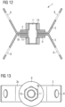
- FIG. 12 shows a schematic sectional view of an electronic component according to a further embodiment.
- Figure 13 shows a perspective view of a portion of the electronic component according to Figure 12 .
- the contact elements 3 are as in connection with Figure 4 As described, it is double-sided.
- the NTC element 2 is arranged between the first partial area 3a of the contact elements 3 and is electrically and thermally connected to the contact elements 3 via the connecting material 7.
- the screw connection is in contrast to the screw connection according to Figure 2 Insulating.
- the NTC element 2 is designed in a ring shape.
- the NTC element 2 has a round, continuous recess.
- the first partial area 3a of the respective contact element 3 also has a recess in this embodiment.
- the recesses of contact elements 3 and NTC element 2 are designed and arranged to enable the insulating screw connection of the contact elements 3.
- the recesses are provided for the introduction of a threaded rod 11 for screwing the contact elements 3.
- a spacer 9 is arranged, which has a recess 9a ( Figure 13 ).
- the respective spacer is, for example, a PTFE disc.
- the respective spacer has a diameter of 15 mm, for example.
- a spacer 9 is arranged on an upper side of the first partial area 3a of the first or upper contact element 3.
- Another spacer 9 is arranged on a lower side of the first partial area 3a of the second or lower contact element 3.
- a nut 10 is arranged on each of the spacers 9. The threaded rod 11 is guided through the nuts 10, the recesses in the spacers 9, the NTC element 2 and the contact elements 3 for screwing the contact elements 3 together.
- An insulating element 14 is inserted into the recess of the NTC element 2 between the threaded rod 11 and the NTC element 2.
- the insulating element 14 can, for example, comprise AlO x .
- the insulating element 14 is an AlO x tube. This enables an insulating screw connection of the component 1.
- the electrical contacting of component 1 is again carried out as in connection with the Figure 2 described via the electrically conductive connection of the contact elements 3 with the battery cables via the cable lugs 5.
- the cable lugs are screwed to the contact elements 3 via the recesses 8 of the contact elements 3.
Landscapes
- Engineering & Computer Science (AREA)
- Microelectronics & Electronic Packaging (AREA)
- Physics & Mathematics (AREA)
- Electromagnetism (AREA)
- Manufacturing & Machinery (AREA)
- Thermistors And Varistors (AREA)
- Details Of Resistors (AREA)
- Emergency Protection Circuit Devices (AREA)
- Powder Metallurgy (AREA)
Abstract
Description
- Die Erfindung betrifft ein elektronisches Bauelement zur Einschaltstrombegrenzung. Die Erfindung betrifft ferner die Verwendung eines elektronischen Bauelements.
- Start-Stopp Systeme im Automobilbereich (PKW, LKW) stellen eine wesentliche Möglichkeit zur Treibstoffersparnis dar und werden deshalb in nahezu allen neuen Fahrzeugen eingebaut. Bei diesen Systemen muss der Einschaltstrom des Anlassers begrenzt werden, um ein Absinken der Bordnetzspannung zu verhindern, damit insbesondere sicherheitsrelevante Anwendungen (ABS, ESP) ausreichend versorgt werden.
- Für den Startvorgang eines Verbrennungsmotors kann hierfür ein thermisch gesteuerter Einschaltstrombegrenzer (ICL) verwendet werden. Beim Neustart des Verbrennungsmotors nach Sparabschaltung wird durch den Strombedarf des Anlassermotors das 12 V Bordnetz kurzzeitig mit bis zu 1000 A belastet. Übliche 12 V Batterien werden durch diese Zusatzleistung so stark belastet, dass die Netzspannung um mehrere Volt abfällt. Dieser Abfall kann zum Ausfall anderer Verbraucher im Bordnetz führen. Um das zu vermeiden muss der Spannungsabfall vermieden bzw. verringert werden. Zur Verringerung des Spannungsabfalls kann beispielsweise ein NTC (Negative Temperature Coefficient) Bauelement verwendet werden.
- Bei den zu erwartenden Abmaßen von mehr als 1 cm2 Querschnitt und weniger als 1 mm Länge des NTC-Bauelements ist eine flächige Kontaktierung mit einem geringen elektrischen Widerstand nötig. Zudem ist das Bauteil beim Betrieb starken Temperaturschwankungen ausgesetzt, wobei der thermische Ausdehnungskoeffizient der ICL-Keramik deutlich kleiner ist als der Ausdehnungskoeffizient guter elektrischer Leiter (z.B. Kupfer). Die dadurch verursachten thermischen mechanischen Verspannungen können zur Zerstörung des Bauteils führen.
- Eine zu lösende Aufgabe besteht darin, ein verbessertes elektronisches Bauelement zur Einschaltstrombegrenzung sowie die Verwendung eines verbesserten elektronischen Bauelements anzugeben.
- Diese Aufgabe wird durch das elektronische Bauelement gemäß Anspruch 1 und die Verwendung gemäß der Ansprüche 17 bzw. 18 gelöst.
- Gemäß einem Aspekt wird ein elektronisches Bauelement, kurz Bauelement, angegeben. Das elektronische Bauelement ist dazu ausgebildet in einem Einschaltstrombegrenzer verwendet zu werden bzw. als Einschaltstrombegrenzer zu agieren. Das Bauelement weist wenigstens ein NTC-Element auf. Das NTC-Element dient als Funktionselement bzw. Funktionsschicht des Bauelements. Das NTC-Element weist eine NTC-Keramik auf. Das Bauelement kann eine Vielzahl von NTC-Elementen, beispielsweise zwei, drei, fünf oder zehn NTC-Elemente aufweisen. Das NTC-Element kann scheiben- oder plättchenförmig (rund) ausgebildet sein. Das NTC-Element kann aber auch eine rechteckige oder ringförmige Fläche aufweisen.
- Auf dem NTC-Element, vorzugsweise auf einer Oberseite und auf einer Unterseite des NTC-Elements, ist eine Metallisierung angeordnet. Die Metallisierung weist vorzugsweise Silber auf.
- Alternativ dazu kann die Metallisierung auch Kupfer oder Gold aufweisen. Das NTC-Element kann ein monolithisches Bauelement sein. In diesem Fall wird die NTC-Keramik in Presstechnologie hergestellt und anschließend durch Läppen (Feinschleifen von beiden Seiten) in die gewünschte Form bzw. auf die gewünschte Dicke gebracht (Dickschichtmonolith). Alternativ dazu kann das NTC-Element auch als Vielschichtmonolith ausgebildet sein. In diesem Fall werden keramische Folien übereinander gestapelt und gepresst um das NTC-Element bereitzustellen.
- Das Bauelement weist wenigstens zwei elektrisch leitende Kontaktelemente oder Elektroden auf. Die Kontaktelemente sind flächig ausgebildet. Die Kontaktelemente sind ausgebildet und angeordnet zur elektrisch leitenden und thermischen Verbindung mit dem NTC-Element. Das Bauelement kann eine Vielzahl von Kontaktelementen aufweisen, beispielsweise fünf, zehn oder 15 Kontaktelemente, wobei die einzelnen NTC-Elemente dadurch thermisch gut gekoppelt sein müssen.
- Das NTC-Element ist über ein Verbindungsmaterial elektrisch leitend mit dem jeweiligen Kontaktelement verbunden. Das NTC-Element ist über das Verbindungsmaterial auch thermisch mit dem jeweiligen Kontaktelement verbunden. Durch das Verbindungsmaterial wird eine stabile, elektrisch hochleitfähige und mechanisch haltbare Verbindung zwischen dem NTC-Element und den Kontaktelementen ausgebildet.
- Der thermische Ausdehnungskoeffizient des jeweiligen Kontaktelements ist an den thermischen Ausdehnungskoeffizienten des NTC-Elements angepasst. Vorzugsweise sind die thermischen Ausdehnungskoeffizienten von NTC-Element und den Kontaktelementen annähernd gleich.
- Beispielsweise weist das NTC-Element einen thermischen Ausdehnungskoeffizienten zwischen 7 ppm / K und 10 ppm / K auf. Vorzugsweise weist das jeweilige Kontaktelement einen entsprechenden Ausdehnungskoeffizienten auf. Der thermische Ausdehnungskoeffizient des jeweiligen Kontaktelements liegt vorzugsweise im Bereich zwischen 5 ppm / K und 10 ppm / K.
- Durch die Anpassung der thermischen Ausdehnungskoeffizienten wird eine Verringerung bzw. Anpassung der Unterschiede der materialbedingten thermischen Ausdehnung (CTE) von NTC-Element und Kontaktelementen erreicht. Dadurch können durch thermische Ausdehnung verursachten Spannungen verringert oder vermieden werden. Somit wird ein besonders stabiles, zuverlässiges und langlebiges Bauelement zur Verfügung gestellt.
- Gemäß einem Ausführungsbeispiel weist das NTC-Element eine Oberseite und eine Unterseite auf. Oberseite und Unterseite liegen einander gegenüber und sind jeweils von den Stirnseiten des NTC-Elements begrenzt. Die Oberseite und die Unterseite ist jeweils zumindest teilweise durch das jeweilige Kontaktelement elektrisch leitend kontaktiert. Je nach Herstellungsprozess kann insbesondere eine geringe Randschicht bzw. ein geringer Randbereich der Oberseite bzw. der Unterseite unkontaktiert bleiben.
- Die Oberseite und die Unterseite kann aber auch jeweils vollflächig durch das jeweilige Kontaktelement elektrisch leitend kontaktiert. Mit anderen Worten, das NTC-Element ist eingebettet zwischen den beiden Kontaktelementen angeordnet, so dass Ober- und Unterseite jeweils teilweise oder vollständig von einem Kontaktelement bedeckt werden. Dadurch kann eine besonders zuverlässige Kontaktierung des NTC-Elements und eine besonders stabile Verbindung zwischen NTC-Element und Kontaktelementen erzielt werden.
- Gemäß einem Ausführungsbeispiel weist das Kontaktelement einen Materialverbund auf. Mit anderen Worten, das Kontaktelement ist aus mehreren Materialien zusammengesetzt. Das jeweilige Kontaktelement weist vorzugsweise Kupfer auf. Kupfer zeichnet sich durch seine sehr hohe elektrische Leitfähigkeit sowie eine sehr hohe Wärmeleitfähigkeit aus. Zusätzlich weist das Kontaktelement vorzugsweise Invar und / oder Kovar und / oder Molybdän auf. Diese Materialien zeichnen sich durch ihren geringen thermischen Ausdehnungskoeffizienten aus. Vorzugsweise weist das jeweilige Kontaktelement ein gewalztes Kupfer -Invar Blech mit Lagenaufbau aus Kupfer - Invar - Kupfer auf. Durch geeignete Wahl des Dickenverhältnisses von Kupfer- und Invar / Kovar bzw. Molybdän -Schichten des jeweiligen Kotaktelements kann der Ausdehnungskoeffizient an den Ausdehnungskoeffizienten des NTC-Elements angepasst werden. Damit wird ein sehr stabiles und langlebiges Bauelement erzielt.
- Gemäß einem Ausführungsbeispiel weist das Kontaktelement einen Lagenaufbau von Kupfer - Invar - Kupfer mit einem Dickenverhältnis von 10% ≤ Kupfer ≤ 30% - 50% ≤ Invar / Kovar / Molybdän ≤ 80% - 10% ≤ Kupfer ≤ 30% auf. Das bedeutet, dass das Kontaktelement wenigstens drei Lagen aufweist. Eine erste Lage weist vorzugsweise Kupfer auf. Die erste Lage weist eine Dicke oder vertikale Ausdehnung auf, die zwischen 1/10 und 3/10 der Gesamtdicke des Kontaktelements beträgt. Eine zweite Lage weist vorzugsweise Kovar und / oder Invar und / oder Molybdän auf. Die zweite Lage weist eine Dicke auf, die zwischen 5/10 und 8/10 der Gesamtdicke des Kontaktelements beträgt. Die dritte Lage weist eine Dicke auf, die zwischen 1/10 und 3/10 der Gesamtdicke des Kontaktelements beträgt.
- Die Lage des Kontaktelements, welche Invar / Kovar / Molybdän aufweist ist dicker, als diejenige Lage des Kontaktelements, welche Kupfer aufweist. Damit kann der Ausdehnungskoeffizient des Kontaktelements reduziert bzw. an den Ausdehnungskoeffizienten des NTC-Elements angepasst werden.
- Vorzugsweise beträgt das Dickenverhältnis Kupfer - Invar - Kupfer 20% - 60% - 20%. Selbstverständlich sind auch andere Dickenverhältnisse und andere Schichtfolgen und Anzahlen von Schichten sowie der Zusatz von Kovar oder Molybdän vorstellbar um den gewünschten Ausdehnungskoeffizienten zu erzielen.
- Gemäß einem Ausführungsbeispiel weist das Verbindungsmaterial Sintersilber auf. Sintersilber weist eine hohe elektrische und thermische Leitfähigkeit aus. Ferner kann Sintersilber hohen Temperaturen von bis zu 400 °C, beispielsweise 300° C, sowie schnellen und vielen Temperaturwechseln standhalten.
- Im Betriebszustand bzw. heißen Zustand des NTC-Elements können sehr hohe Temperaturen sowie eine Vielzahl von Temperaturwechseln auftreten. Daher ist die Hitzebeständigkeit und Anpassungsfähigkeit des Verbindungsmaterials von äußerster Wichtigkeit. Der heiße Zustand bezeichnet dabei einen Zustand bei einer Temperatur, welche größer ist als diejenige des NTC-Elements in einem Grundzustand. Der Temperaturbereich zwischen dem Grundzustand und dem heißen Zustand kann beispielsweise jeden Temperaturbereich zwischen -55°C und +300°C überspannen oder sich über diesen Bereich erstrecken. Bevorzugt kann sich der Temperaturbereich zwischen dem Grundzustand und dem heißen Zustand über den Bereich von -40°C bis +300°C erstrecken.
- Bevorzugt weist das Verbindungsmaterial µAg auf. µAg zeichnet sich insbesondere durch seine ausreichende Porösität aus.
- Gemäß einem Ausführungsbeispiel weist das NTC-Element zwei, drei, fünf, zehn oder mehr Segmente auf. Die Segmente des NTC-Elements stellen vorzugsweise rechteckige Teilbereiche des NTC-Elements dar, die voneinander beabstandet sind. Der Abstand zwischen den Segmenten beträgt 0,05 mm bis 0,2 mm, beispielsweise 0,1 mm. Mit anderen Worten, zwischen den einzelnen Segmenten befinden sich Fugen (Dehnungsfugen). Durch diese Dehnungsfugen werden keine oder nur geringe Verspannungen aufgebaut. Zusätzliche mechanische Spannungen können somit vermieden werden und folglich kann ein langlebiges Bauelement zu Verfügung gestellt werden.
- Gemäß einem Ausführungsbeispiel weist das NTC-Element bei einer Temperatur von 25°C (Raumtemperatur) einen Nominalwiderstand R25 ≤ 1 Ω auf. Als Raumtemperatur wird hierbei die Temperatur verstanden, die üblicherweise in bewohnten Räumen herrscht. Der genannte elektrische Widerstand beschreibt vorzugsweise den elektrischen Widerstand des unbelasteten NTC-Elements zwischen Außenkontakten bei einer Umgebungstemperatur von 25°C.
- Beispielsweise weist das NTC-Element bei der angegeben Temperatur einen Nominalwiderstand R25 von kleiner oder gleich 0,1 Ω auf, vorzugsweise kleiner 0,05 Ω. Das NTC-Element weist folglich einen sehr kleinen elektrischen Widerstand bei Raumtemperatur bzw. bei 25°C und damit eine sehr hohe elektrische Leitfähigkeit auf. Damit ist das NTC-Element besonders gut zum Einsatz in einem Einschaltstrombegrenzer mit hoher Stromlast geeignet.
- Durch den geringen elektrischen Widerstand kann insbesondere erreicht werden, dass ein ausreichend hoher Einschaltstrom eines elektrischen Verbrauchers, welcher beispielsweise in einer entsprechenden Anwendung in Reihe zu dem elektronischen Bauelement geschaltet ist, zur Verfügung gestellt wird, aber soweit begrenzt wird, dass beispielsweise die elektrische Spannung beim Einschaltvorgang für die elektrische Versorgung weiterer wichtiger elektrischer Komponenten noch ausreichend hoch ist. Mit Hilfe des Bauelements wird der Spannungseinbruch beim Startvorgang des Verbrauchers im Vergleich zu einem Verbraucher ohne das elektronische Bauelement vorzugsweise um ca. 1 V reduziert.
- Gemäß einem Ausführungsbeispiel ist der spezifische elektrische Widerstand des NTC-Elements in einem Grundzustand des elektronischen Bauelements ≤ 2 Ωcm. Vorzugsweise liegt der spezifische elektrische Widerstand des NTC-Elements in einem Grundzustand des elektronischen Bauelements zwischen 0,1 Ωcm und 1,0 Ωcm, beispielsweise bei 0,3 Ωcm.
- Gemäß einem Ausführungsbeispiel weist das Kontaktelement eine Dicke d auf. Vorzugsweise gilt 0,3 mm ≤ d ≤ 0,8 mm. Bevorzugt beträgt die Dicke d des jeweiligen Kontaktelements weniger als 0,7 mm, beispielsweise 0,6 mm.
- Gemäß einem Ausführungsbeispiel weist das Bauelement eine Vielzahl von NTC-Elementen und Kontaktelementen auf. Die mehreren NTC-Elemente können durch Vereinzeln aus einem Substrat bereitgestellt werden. Die NTC-Elemente sind zueinander parallel geschaltet. Die Strombelastbarkeit und/oder Stromtragfähigkeit des Bauelements kann durch eine Parallelschaltung von mehreren NTC-Elementen gesteigert werden. Vorzugsweise sind die NTC-Elemente stapelförmig übereinander angeordnet. Zwischen zwei benachbarten NTC-Elementen ist jeweils ein Kontaktelement angeordnet. Die NTC-Elemente sind über die Kontaktelemente thermisch gut aneinander gekoppelt.
- Gemäß einem Ausführungsbeispiel weist das NTC-Element die Zusammensetzung La(1-x)EA(x)Mn(1-a-b-c)Fe(a)Co(b)Ni(c)O(3±δ) auf. Dabei ist 0 ≤ x ≤ 0,5 und 0 ≤ (a+b+c) ≤ 0,5. EA bezeichnet ein Erdalkali-Element. Vorzugsweise wird das Erdalkali-Element aus Magnesium, Calcium, Strontium oder Barium ausgewählt. δ bezeichnet die Abweichung vom stöchiometrischen Sauerstoffverhältnis (Sauerstoffüberschuss bzw. Sauerstoffdefizit). Vorzugsweise ist |δ| ≤ 0,5. Besonders bevorzugt ist |δ| = 0.
- Durch diese Zusammensetzung wird ein NTC-Element bereitgestellt, welches sich durch eine außerordentlich hohe elektrische Leitfähigkeit und einen ausreichenden B-Wert (Thermistorkonstante) auszeichnet. Durch (eine) spezifische Dicke und (einen) spezifischen Querschnitt bzw. Fläche des NTC-Elements kann der Widerstand weiter variiert und gesteuert werden. Das NTC-Element weist eine Dicke d auf. Vorzugsweise gilt 100 µm ≤ d ≤ 600 µm. Bevorzugt beträgt die Dicke d des NTC-Elements weniger als 500 µm, beispielsweise 400 µm. Der B-Wert B25/100 liegt im Bereich zwischen 1000 K und 4000 K, bevorzugt zwischen 1400 K und 2000 K, beispielsweise bei 1500 K.
- Gemäß einem Ausführungsbeispiel weist das Bauelement ein Befestigungselement auf. Das Befestigungselement ist vorzugsweise dazu ausgebildet und angeordnet eine elektrisch leitendende Verbindung mit Batterieleitungen herzustellen. Das Befestigungselement ist ferner vorzugsweise dazu ausgebildet und angeordnet eine mechanische Verbindung mit Batterieleitungen herzustellen. Das Befestigungselement ist ferner vorzugsweise dazu ausgebildet und angeordnet eine - indirekte - mechanische Verbindung zwischen den Kontaktelementen bereitzustellen.
- Das Befestigungselement kann dazu ausgebildet sein, eine Schraubverbindung auszubilden. Das Befestigungselement kann beispielsweise aber auch dazu ausgebildet sein eine Klemmverbindung auszubilden. Das Befestigungselement kann ferner ein Dichtelement aufweisen. Das Dichtelement kann isolierend oder teilweise isolierend ausgebildet sein. Das Befestigungselement kann wenigstens eine Mutter und eine Schraube und / oder wenigstens ein Klemmelement, beispielsweise zwei Klemmelemente, aufweisen.
- Das Befestigungselement weist einen elektrischen Widerstand auf. Der elektrische Widerstand ist gleich bzw. nur geringfügig höher, als der Widerstand des NTC-Elements bei tiefen Betriebstemperaturen. Insbesondere ist der elektrische Widerstand des Befestigungselements gleich bzw. nur geringfügig höher, als der Widerstand des NTC-Elements bei der untersten Betriebstemperatur, z.B. -40°C.
- Der Widerstand des Befestigungselements ist nicht temperaturabhängig. Dadurch ist auch in einem Fehlerfall (z.B. Bruch der leitfähigen Verbindung zwischen NTC-Element und Kontaktelement) noch immer ein Start des Motors möglich (abhängig von der Auslegung des Anlassersystems). Der Spannungseinbruch wird ebenfalls vermieden, jedoch wird die zum Starten verfügbare elektrische Leistung stark begrenzt wodurch der Startvorgang u.U. deutlich verzögert wird. Neben einer Verschraubung kann auch ein Fixwiderstand oder eine anderes leitfähiges Element mit definiertem elektrischem Widerstand als Befestigungselement verwendet werden.
- Gemäß einem weiteren Aspekt wird die Verwendung eines elektronischen Bauelements beschrieben. Vorzugsweise wird die Verwendung des oben beschriebenen Bauelements angegeben. Alle Merkmale, die in Zusammenhang mit dem Bauelement erläutert wurden, gelten auch für die Verwendung und umgekehrt.
- Es wird insbesondere die Verwendung des oben beschriebenen Bauelements für Start- / Stopp- Systeme im Automobilbereich angegeben. Durch den temperaturabhängigen Widerstand (NTC-Element) wird der Einschaltstrom beim Einschalten begrenzt. Beim Einschalten erwärmt sich das NTC-Element sofort durch den Einschaltstrom (z.B. auf 250°C), wodurch sich der NTC Widerstand schnell bis auf einen sehr kleinen Restwiderstand verringert(z.B. 0,5 mΩ). Diese dynamische Widerstandsänderung verringert auf Grund der spezifischen Eigenschaften des NTC-Elements die vom Anlassermotor verursachte Stromspitze, was gleichzeitig den Spannungseinbruch der Batterie verringert. Damit wird ein effektives Bauelement zur Einschaltstrombegrenzung in Start-Stopp-Systemen bereitgestellt.
- Durch die bereitgestellten Kontaktelemente und das Verbindungsmaterial wird ferner eine sehr niederohmige elektrischen Verbindung von NTC-Element zu den Kontaktelementen für wiederholte Schaltzyklen realisiert, bei denen die Umgebungstemperatur von -40°C bis 120°C schwanken kann. Beim Schaltzyklus kann die Temperatur auf bis zu 300°C steigen. Somit wird ein stabiles, elektrisch hochleitfähiges Bauelement mit mechanisch haltbarer, temperatur-beständiger und extrem belastbarer Verbindung zwischen NTC-Element und Kontaktelementen zur Verwendung für Start- / Stopp- Systeme im Automobilbereich angegeben.
- Gemäß einem weiteren Aspekt wird die Verwendung eines elektronischen, insbesondere des oben beschriebenen elektronischen Bauelements, für Ströme bis 1000 A bei Gleichspannung in 12 V und 24 V Netzen angegeben.
- Im Folgenden sind vorteilhafte Aspekte beschrieben. Um eine Referenzierung zu erleichtern sind die Aspekte durchnummeriert. Merkmale der Aspekte sind nicht nur in Kombination mit dem speziellen Aspekt, auf den sie sich beziehen, sondern auch separat betrachtet relevant.
- 1. Elektronisches Bauelement zur Einschaltstrombegrenzung aufweisend
- wenigstens ein NTC-Element,
- wenigstens zwei elektrisch leitende Kontaktelemente,
- 2. Elektronisches Bauelement nach Aspekt 1,
wobei das NTC-Element eine Oberseite und eine Unterseite aufweist, und wobei die Oberseite und die Unterseite zumindest teilweise durch das jeweilige Kontaktelement elektrisch leitend kontaktiert sind. - 3. Elektronisches Bauelement nach Aspekt 1 oder 2,
wobei das Kontaktelement einen Materialverbund aufweist. - 4. Elektronisches Bauelement nach einem der vorangehenden Aspekte,
wobei das Kontaktelement Kupfer aufweist und wobei das Kontaktelement Invar oder Kovar aufweist. - 5. Elektronisches Bauelement nach einem der vorangehenden Aspekte,
wobei das Kontaktelement einen Lagenaufbau von Kupfer -Invar - Kupfer mit einem Dickenverhältnis von 10% ≤ Kupfer ≤ 30% - 50% ≤ Invar / Kovar ≤ 80% - 10% ≤ Kupfer ≤ 30% aufweist. - 6. Elektronisches Bauelement nach einem der vorangehenden Aspekte,
wobei das Verbindungsmaterial Sintersilber aufweist. - 7. Elektronisches Bauelement nach einem der vorangehenden Aspekte,
wobei das NTC-Element zwei, drei oder mehr Segmente aufweist. - 8. Elektronisches Bauelement nach einem der vorangehenden Aspekte,
wobei das NTC-Element bei einer Temperatur von 25°C einen Nominalwiderstand R25 ≤ 1 Ω aufweist. - 9. Elektronisches Bauelement nach einem der vorangehenden Aspekte,
wobei der spezifische elektrische Widerstand des NTC-Elements in einem Grundzustand des elektronischen Bauelements ≤ 2 Ωcm ist. - 10. Elektronisches Bauelement nach einem der vorangehenden Aspekte,
wobei das Kontaktelement eine Dicke d aufweist, und wobei 0,3 mm ≤ d ≤ 0,8 mm. - 11. Elektronisches Bauelement nach einem der vorangehenden Aspekte,
wobei das NTC-Element eine Dicke d aufweist, und wobei 100 µm ≤ d ≤ 600 µm. - 12. Elektronisches Bauelement nach einem der vorangehenden Aspekte,
aufweisend eine Vielzahl von NTC-Elementen und Kontaktelementen, wobei die NTC-Elemente zueinander parallel geschaltet sind. - 13. Elektronisches Bauelement nach Aspekt 12,
wobei die NTC-Elemente stapelförmig übereinander angeordnet sind, wobei zwischen zwei benachbarten NTC-Elementen jeweils ein Kontaktelement angeordnet ist und wobei die NTC-Elemente über die Kontaktelemente thermisch aneinander gekoppelt sind. - 14. Elektronisches Bauelement nach einem der vorangehenden Aspekte,
- wobei das NTC-Element die Zusammensetzung La(1-x)EA(x)Mn(1-a-b-c)Fe(a)Co(b)Ni(c)O(3±δ) aufweist,
- wobei 0 ≤ x ≤ 0,5 und 0 ≤ (a+b+c) ≤ 0,5 und wobei EA ein Erdalkali-Element und δ eine Abweichung von einem stöchiometrischen Sauerstoffverhältnis bezeichnet, wobei das Erdalkali-Element (EA) ausgewählt ist aus Magnesium, Calcium, Strontium oder Barium und/oder wobei |δ| ≤ 0,5 beträgt.
- 15. Elektronisches Bauelement nach einem der vorangehenden Aspekte,
wobei das NTC-Element einen thermischen Ausdehnungskoeffizienten zwischen 7 ppm / K und 10 ppm / K aufweist. - 16. Elektronisches Bauelement nach einem der vorangehenden Aspekte
aufweisend ein Befestigungselement, wobei das Befestigungselement einen elektrischen Widerstand aufweist welcher gleich bzw. nur geringfügig höher ist, als der Widerstand des NTC-Elements bei tiefen Betriebs-temperaturen. - 17. Verwendung eines elektronischen Bauelements gemäß einem der Aspekte 1 bis 16 für Start- / Stopp- Systeme im Automobilbereich.
- 18. Verwendung eines elektronischen Bauelements gemäß einem der Aspekte 1 bis 16 für Ströme bis 1000 A bei Gleichspannung in 12 V und 24 V Netzen.
- Die Erfindung wird im Folgenden anhand von Ausführungsbeispielen und den dazugehörigen Figuren näher erläutert.
- Die nachfolgend beschriebenen Zeichnungen sind nicht als maßstabsgetreu aufzufassen. Vielmehr können zur besseren Darstellung einzelne Dimensionen vergrößert, verkleinert oder auch verzerrt dargestellt sein.
- Elemente, die einander gleichen oder die die gleiche Funktion übernehmen, sind mit gleichen Bezugszeichen bezeichnet.
- Figur 1
- zeigt eine schematische Schnittansicht eines elektronischen Bauelements.
- Figur 2
- zeigt eine perspektivische Ansicht einer möglichen Kontaktierung des elektronischen Bauelements gemäß
Figur 1 , - Figur 3
- zeigt eine perspektivische Ansicht eines elektronischen Bauelements gemäß einem weiteren Ausführungsbeispiel,
- Figur 4
- zeigt eine schematische Schnittansicht eines elektronischen Bauelements gemäß einem weiteren Ausführungsbeispiel,
- Figur 5
- zeigt eine perspektivische Ansicht einer möglichen Kontaktierung des elektronischen Bauelements gemäß
Figur 4 , - Figur 6
- zeigt eine schematische Schnittansicht eines elektronischen Bauelements gemäß einem weiteren Ausführungsbeispiel,
- Figur 7
- zeigt eine perspektivische Ansicht eines elektronischen Bauelements gemäß einem weiteren Ausführungsbeispiel,
- Figur 8
- zeigt eine schematische Schnittansicht eines elektronischen Bauelements gemäß einem weiteren Ausführungsbeispiel,
- Figur 9
- zeigt eine Draufsicht auf einen Teilbereich des elektronischen Bauelements gemäß
Figur 8 , - Figur 10
- zeigt eine schematische Schnittansicht eines elektronischen Bauelements gemäß einem weiteren Ausführungsbeispiel,
- Figur 11
- zeigt eine Draufsicht auf einen Teilbereich des elektronischen Bauelements gemäß
Figur 10 , - Figur 12
- zeigt eine schematische Schnittansicht eines elektronischen Bauelements gemäß einem weiteren Ausführungsbeispiel,
- Figur 13
- zeigt eine Draufsicht auf einen Teilbereich des elektronischen Bauelements gemäß
Figur 12 . - Die
Figur 1 zeigt ein elektronisches Bauelement 1, kurz Bauelement 1. Das Bauelement 1 ist dazu ausgebildet als Einschaltstrombegrenzer oder in einem Einschaltstrombegrenzer für Start- / Stopp- Systeme in 12 V und 24 V Netzen im Automobilbereich eingesetzt zu werden. Das Bauelement 1 ist insbesondere für eine Verwendung bei Strömen bis 1000 A (bei Gleichspannung in 12 V und 24 V Netzen) geeignet. Das Bauelement 1 dazu geeignet in typischen 12 V Startermotoren mit ca. 1 kW bis 3 kW Leistung verwendet zu werden. - Das Bauelement 1 weist ein NTC-Element 2 bzw. eine NTC-Keramik auf. Das NTC-Element 2 stellt eine Funktionsschicht bzw. ein Funktionselement des Bauelements 1 dar. Das NTC-Element 2 ist ein heißleitendes Bauelement mit einem negativen Temperaturkoeffizienten.
- Das NTC-Element 2 weist eine Materialzusammensetzung auf, welche sich durch eine hohe elektrische Leitfähigkeit bzw. einen geringen spezifischen Widerstand auszeichnet.
- Das NTC-Element 2 weist vorzugsweise die folgende Zusammensetzung auf: La(1-x)EA(x)Mn(1-a-b-c)Fe(a)Co(b)Ni(c)O(3±δ). Dabei gilt 0 ≤ x ≤ 0,5 und 0 ≤ (a+b+c) ≤ 0,5. EA steht für ein Erdalkali-Element, beispielsweise Mg, Ca, Sr oder Ba. δ bezeichnet die Abweichung vom stöchiometrischen Sauerstoffverhältnis (Sauerstoffüberschuss bzw. Sauerstoffdefizit). Vorzugsweise ist |δ| ≤ 0,5, besonders bevorzugt ist |δ| = 0. Beispielsweise weist die NTC-Keramik die Zusammensetzung La0,95Sr0,05MnO3 auf.
- Der spezifische elektrische Widerstand des NTC-Elements 2 in einem Grundzustand des NTC-Elements 2 beträgt kleiner oder gleich 2 Ωcm, bevorzugt ≤ 1 Ωcm, beispielsweise 0,5 Ωcm. Der Grundzustand beschreibt dabei eine Temperatur des NTC-Elements 2 von 25°C bzw. bei Raumtemperatur. Bei dem Grundzustand kann es sich um einen unbelasteten Zustand, in dem beispielsweise keine elektrische Leistung an dem NTC-Element 2 angelegt ist, handeln.
- Das NTC-Element 2 weist bei der angegeben Temperatur einen elektrischen Widerstand (Nominalwiderstand R25) von kleiner oder gleich 1 Ω auf, vorzugsweise kleiner 0,1 Ω, beispielsweise 0,05 Ω. Das NTC-Element 2 weist folglich einen geringen elektrischen Widerstand bei Raumtemperatur bzw. bei 25°C und damit eine hohe elektrische Leitfähigkeit auf. Damit ist das NTC-Element 2 besonders gut zum Einsatz in einem Einschaltstrombegrenzer geeignet.
- Das NTC-Element 2 weist ferner einen hohen B-Wert auf. Der B-Wert B25/100 liegt im Bereich zwischen 1000 K und 4000 K, bevorzugt zwischen 1400 K und 2000 K, beispielsweise bei 1500 K. Das NTC-Element 2 hat einen geringen thermischen Ausdehnungskoeffizienten. Typischerweise liegt der thermische Ausdehnungskoeffizient des NTC-Elements 2 zwischen 7 ppm / K und 10 ppm / K.
- Das NTC-Element 2 ist vorzugsweise als monolithisches Bauelement ausgebildet. Beispielsweise ist das NTC-Element 2 ein Dickschichtmonolith. In diesem Fall wird das NTC-Element 2 in Presstechnologie hergestellt und anschließend durch Läppen (Feinschleifen von beiden Seiten) auf die gewünschte Dicke gebracht. Alternativ dazu kann das NTC-Element 2 aber auch als Vielschichtmonolith ausgebildet sein. In diesem Fall werden keramische Folien übereinander gestapelt und gepresst um das NTC-Element 2 bereitzustellen.
- Das in
Figur 2 dargestellte NTC-Element 2 hat eine runde Form. Das NTC-Element 2 ist scheibenförmig oder plättchenförmig ausgebildet. Aber auch andere Formen sind für das NTC-Element 2 vorstellbar, beispielsweise eine rechteckige Form oder eine Ringform. Das NTC-Element 2 kann in Form eines Substrats ausgebildet sein. Das NTC-Element 2 weist eine Fläche zwischen 25 mm2 und 500 mm2, beispielsweise 200 mm2 auf. Der Durchmesser des NTC-Elements 2 beträgt beispielsweise kleiner oder gleich 14 mm, z.B. 13,75 mm. Das NTC-Element 2 weist eine Dicke d zwischen 100 µm und 600 µm, beispielsweise 400 µm, auf. Durch Variieren von Dicke d und / oder Querschnitt bzw. Fläche des NTC-Elements 2 kann der Widerstand des NTC-Elements 2 variiert und gesteuert werden. - Das NTC-Element 2 weist eine Metallisierung auf (nicht explizit dargestellt). Die Metallisierung ist vorzugsweise an einer Oberseite und an einer Unterseite des NTC-Elements 2 angeordnet. Vorzugsweise weist die Metallisierung eingebranntes Silber auf.
- Das Bauelement 1 weist ferner zwei Kontakte 3 bzw. Kontaktelemente 3 auf (Pluskontakt- und Minuskontaktelement 12b, 12a, siehe
Figur 3 ). Die Kontaktelemente 3 dienen der elektrischen Kontaktierung des NTC-Elements 2. Die Kontaktelemente 3 liegen in diesem Ausführungsbeispiel vollflächig auf der Oberseite und der Unterseite des NTC-Elements 2 auf. Alternativ dazu (nicht explizit dargestellt) kann ein schmaler Randbereich von Oberseite und Unterseite auch frei von dem jeweiligen Kontaktelement 3 bleiben. - Die Kontaktelemente 3 sind jeweils mit der Oberseite und der Unterseite des NTC-Elements 2 elektrisch leitend verbunden. Vorzugsweise sind das NTC-Element 2 und die Kontaktelemente 3 versintert.
- Zu diesem Zweck weist das Bauelement 1 ein Verbindungsmaterial 7 auf. Zwischen der Oberseite des NTC-Elements 2 und dem ersten Kontaktelement 3 sowie zwischen der Unterseite des NTC-Elements 2 und dem zweiten Kontaktelement 7 ist jeweils eine Schicht aus Verbindungsmaterial 7 ausgebildet. Die Schichtdicke des Verbindungsmaterials 7 liegt vorzugsweise im Bereich zwischen 15 µm und 80 µm, beispielsweise bei 20 µm.
- Das Verbindungsmaterial 7 zeichnet sich durch eine hohe elektrische und thermische Leitfähigkeit aus. Das Verbindungsmaterial 7 zeichnet sich ferner vorzugsweise durch eine große Porösität aus. Das Verbindungsmaterial 7 zeichnet sich ferner dadurch aus, dass es hohen Temperaturen bis zu 400 °C, z.B. 300°C, sowie vielen und schnellen Temperaturwechseln standhalten kann, die im Betrieb bzw. im heißen Zustand des Bauelements 1 auftreten können.
- Der heiße Zustand bezeichnet dabei einen Zustand des Bauelements 1 bei einer Temperatur, welche größer ist als diejenige des Bauelements 1 in dem Grundzustand. Der Temperaturbereich zwischen dem Grundzustand und dem heißen Zustand kann beispielsweise jeden Temperaturbereich zwischen -55°C und +300°C überspannen oder sich über diesen Bereich erstrecken. Bevorzugt kann sich der Temperaturbereich zwischen dem Grundzustand und dem heißen Zustand über den Bereich von -40°C bis +300°C erstrecken.
- Beispielsweise weist das Verbindungsmaterial 7 Sintersilber Ag oder µAg auf. Sintersilber hat den Vorteil, dass es eine ausreichende Porösität auf weist. Mit Hilfe des Verbindungsmaterials 7 wird eine stabile, elektrisch hoch leitfähige sowie mechanisch haltbare Verbindung zwischen dem NTC-Element 2 und den Kontaktelementen 3 erzielt.
- Das jeweilige Kontaktelement 3 weist eine hohe thermische und elektrische Leitfähigkeit auf. Das jeweilige Kontaktelement 3 ist ferner so ausgebildet, dass thermische Spannungen zwischen dem NTC-Element 2 und dem Kontaktelement 3 reduziert werden. Insbesondere ist das jeweilige Kontaktelement 3 dazu ausgebildet die Unterschiede der materialbedingten thermischen Ausdehnung (CTE) zu verringern bzw. zu reduzieren.
- Vorzugsweise weist das jeweilige Kontaktelement 3 einen Materialverbund auf. Das jeweilige Kontaktelement kann beispielsweise als Verbundblech ausgebildet sein. Der Materialverbund kann Kupfer-Invar-Kupfer (CIC) aufweisen. An Stelle von Invar kann auch Kovar oder Molybdän als Material verwendet werden. Invar bzw. Kovar bzw. Molybdän hat einen geringen thermischen Ausdehnungskoeffizienten. Typischerweise liegt der thermische Ausdehnungskoeffizient dieser Materialien bei ≤ 10 ppm / K, beispielsweise bei 7 ppm / K. Damit ist der Ausdehnungskoeffizient von Kovar / Invar / Molybdän sehr ähnlich zu dem Ausdehnungskoeffizienten des NTC-Elements 2. Durch eine geeignete Wahl des Dickenverhältnisses der Schichten des Materialverbunds kann der Ausdehnungskoeffizient des Kontaktelements 3 gut an den Ausdehnungskoeffizienten des NTC-Elements 2 angepasst werden. Thermische Spannungen können reduziert oder vermieden werden.
- In diesem Ausführungsbeispiel ist das jeweilige Kontaktelement 3 ein gewalztes Kupfer-Invar Blech mit Lagenaufbau aus Kupfer-Invar-Kupfer von 20%-60%-20%. Jedoch sind auch andere Verhältnisse von Kupfer und Invar oder Kovar / Molybdän vorstellbar. Insbesondere können je nach erforderlicher Fläche des NTC-Elements 2 sowie dem erforderlichen Wärmeleitwiderstand auch andere Schichtfolgen und Schichtdicken zum Einsatz kommen.
- Die Kontaktelemente 3 umschließen das NTC-Element 2 zangenförmig. Dabei liegt ein erster Teilbereich 3a des jeweiligen Kontaktelements 3 an der Oberseite bzw. Unterseite des NTC-Elements 2 auf und verläuft parallel zu der Oberseite bzw. Unterseite des NTC-Elements 2 bzw. zu einer Längsachse L des Bauelements 1. Eine Länge bzw. horizontale Ausdehnung des NTC-Elements 2 ist vorzugsweise kleiner oder gleich der Länge oder horizontalen Ausdehnung des ersten Teilbereichs 3a.
- Ein zweiter Teilbereich 3b des jeweiligen Kontaktelements 3 schließt einen Winkel mit der Längsachse L ein. Der zweite Teilbereich 3b schließt sich vorzugsweise in einem Winkel von ≤ 20 °, beispielsweise 15°, zur Längsachse L des Bauelements 1 an den ersten Teilbereich 3a an. Der Winkel zwischen dem zweiten Teilbereich 3b des ersten Kontaktelements 3 und dem zweiten Teilbereich 3b des zweiten Kontaktelements beträgt vorzugsweise kleiner oder gleich 40°, beispielsweise 30°. Ein dritter Teilbereich 3c des jeweiligen Kontaktelements 3 schließt sich an den zweiten Teilbereich 3b an und verläuft parallel zur Längsachse L.
- Die jeweiligen Teilbereiche 3a, 3b, 3c weisen in diesem Ausführungsbeispiel vorzugsweise die gleiche Länge auf. Beispielsweise weiden die Teilbereiche 3a, 3b, 3c jeweils eine Länge von 10 mm bis 15 mm auf. Die jeweiligen Teilbereiche 3a, 3b, 3c weisen vorzugsweise die gleiche Dicke d auf. Beispielsweise weiden die Teilbereiche 3a, 3b, 3c jeweils eine Dicke d von kleiner oder gleich 0,8 mm und größer oder gleich 0,3 mm auf. Folglich beläuft sich die Dicke d des jeweiligen Kontaktelements 3 auf 0,3 mm ≤ d ≤ 0,8 mm, beispielsweise d = 0,7 mm.
- Die Teilbereiche 3a, 3b, 3c gehen ineinander über. Mit anderen Worten, die Teilbereiche 3a, 3b, 3c sind nicht als separate Bereiche bzw. Bauteile ausgeführt sondern stellen nur Unterabschnitte des jeweiligen Kontaktelements 3 dar.
- Das jeweilige Kontaktelement 3, insbesondere der dritte Teilbereich 3c, weist eine Aussparung 8 auf. Vorzugsweise weist der dritte Teilbereich 3c dafür eine größere horizontale Ausdehnung bzw. eine größere Fläche auf, als der erste und zweite Teilbereich 3a, 3b (siehe beispielsweise
Figur 3 ). Die Aussparung 8 ist vorzugsweise kreisförmig ausgebildet. Die Aussparung 8 weist beispielsweise einen Durchmesser von 8 mm auf. Die Aussparung 8 durchdringt das Kontaktelement 3 vollständig. Die Aussparung 8 dient dazu das Bauelement 1 mittels eines Befestigungselements mit Batterieleitungen zu verbinden, wie beispielsweise in Zusammenhang mitFigur 2 näher erläutert wird. - Die
Figur 2 zeigt eine mögliche Kontaktierung des Bauelements 1 gemäß derFigur 1 mit den Batterieleitungen über Kabelschuhe. - Das Bauelement 1 weist ein Befestigungselement zur Herstellung der elektrischen Kontaktierung des Bauelements 1 und insbesondere zur mechanischen Befestigung von Batterieleitungen mit dem Bauelement 1 auf. Das Befestigungselement kann zur Bereitstellung einer wie nachfolgend beschriebenen Schraubverbindung ausgebildet sein. Alternativ dazu kann das Befestigungselement auch dazu ausgebildet und angeordnet sein eine Klemmverbindung herzustellen.
- Zwischen dem ersten und zweiten Kontaktelement 3 ist ein Distanzhalter 9 angeordnet. Der Distanzhalter 9 ist zwischen einer Unterseite des dritten Teilbereichs 3c des ersten bzw. oberen Kontaktelements 3 und der Oberseite des dritten Teilbereichs 3c des zweiten bzw. unteren Kontaktelements 3 angeordnet. Der Distanzhalter 9 ist zylinderförmig ausgebildet.
- Der Distanzhalter 9 ist isolierend ausgebildet. Der Distanzhalter 9 dient der elektrischen Isolierung zwischen den beiden Kontaktelementen 3 (Pluskontaktelement 12b und Minuskontaktelement 12a, siehe
Figur 3 ). Der Distanzhalter 9 weist beispielsweise Polytetrafluorethylen (PTFE) auf. PTFE hat den Vorteil, dass es bis zu einer Temperatur von ca. 250° C beständig isolierend ist. Vorzugsweise weist der Distanzhalter 9 eine Aussparung auf (nicht explizit dargestellt), welche den Distanzhalter 9 in vertikaler Richtung vollständig durchdringt. Die Aussparung dient zur Aufnahme eines Verbindungselements, z.B. einer Gewindestange 11, beispielsweise einer Schraube. - An der Oberseite des ersten Kontaktelements 3 bzw. der Unterseite des zweiten Kontaktelements 3 ist jeweils eine Mutter 10 angeordnet. Gewindestange 11 und Muttern 10 dienen zur Verschraubung der Kontaktelemente 3 und zur elektrisch leitenden und mechanischen Verbindung des Bauelements 1 mit den Batterieleitungen (nicht explizit dargestellt). Alternativ dazu beispielsweise Klemmelemente bereitgestellt werden zur Verklemmung der Kontaktelemente 3 und / oder zur elektrisch leitenden und mechanischen Verbindung des Bauelements 1 mit den Batterieleitungen (nicht explizit dargestellt).
- Zwischen den nicht dargestellten Batterieleitungen und den Kontaktelementen 3 sind Kabelschuhe 5 angeordnet, an denen ein nicht dargestelltes Kupferkabel befestigt ist. Die Kabelschuhe 5 sind elektrisch leitend mit den Kontaktelementen 3 verbunden. Zur Verbindung des Bauelements 1 mit den Kabelschuhen 5 wird die Gewindestange 11 durch die Muttern 10, die Aussparung 8 im jeweiligen Kontaktelement 3 sowie die Aussparung im Distanzhalter 9 geführt.
- Die Verschraubung auf einer Achse vermeidet dabei zusätzliche mechanische Spannungen auf die Verbindung zwischen dem NTC-Element 2 und den Kontaktelementen 3. Die Verschraubung bzw. Befestigung muss entweder einen höheren Widerstand als das NTC-Element 2 aufweisen oder muss isolierend ausgeführt sein (siehe beispielsweise
Figuren 12 und 13 ). Die Verschraubung bzw. Befestigung kann alternativ auch direkt auf einen Massekontakt am Fahrzeug oder des Anlassermotors erfolgen. - Durch den temperaturabhängigen Widerstand des Bauelements 1 wird der Einschaltstrom beim Einschalten begrenzt. Beim Einschalten erwärmt sich das NTC-Element 2 sofort durch den Einschaltstrom (z.B. auf 250°C), wodurch sich der NTC Widerstand schnell bis auf einen sehr kleinen Restwiderstand (z.B. 0,5 mΩ) verringert. Diese dynamische Widerstandsänderung verringert die vom Anlassermotor verursachte Stromspitze, was gleichzeitig den Spannungseinbruch der Batterie verringert. Damit wird ein stabiles, langlebiges und effizientes Bauelement zur Einschaltstrombegrenzung zur Verfügung gestellt.
- Das Bauelement 1 kann zusätzlich mit einer so genannten "fail-safe" (Fehlerausfall) Funktion ausgestattet werden. Dazu wird die in
Figur 2 gezeigte Verschraubung so ausgeführt, dass ihr elektrischer Widerstand gleich bzw. nur geringfügig höher ist, als der Widerstand des NTC-Elements 2 bei der untersten Betriebstemperatur, z.B. -40°C. Der Widerstand dieser Verschraubung ist nicht temperaturabhängig. Dadurch ist auch in einem Fehlerfall (z.B. Bruch der leitfähigen Verbindung zwischen NTC-Element 2 und Kontaktelement 3) noch immer ein Start des Motors möglich (abhängig von der Auslegung des Anlassersystems). Der Spannungseinbruch wird ebenfalls vermieden, jedoch wird die zum Starten verfügbare elektrische Leistung stark begrenzt, wodurch der Startvorgang unter Umständen deutlich verzögert wird. - Beispielsweise beträgt der spezifische elektrische Widerstand des NTC-Elements 2 bei 25°C: Rspez,25 = 0,2 Ωcm. Der Nominalwiderstand R25 des NTC-Elements 2 bei einer Temperatur von 25°C beträgt beispielsweise R25 = 10 mΩ. Der B-Wert liegt beispielsweise bei 1650 K. Damit ergibt sich für einen spezifischen elektrischen Widerstand des NTC-Elements 2 bei einer Temperatur von -40°C Rspez,-40 = 0,65 Ωcm und für einen Widerstand des NTC-Elements 2 von 32 mΩ ein elektrischer Widerstand der Verschraubung von vorzugsweise 32 bis 35 mΩ.
- Alternativ zu einer Verschraubung kann auch ein Fixwiderstand oder eine anderes leitfähiges Element mit definiertem elektrischem Widerstand verwendet werden.
- Die
Figur 3 zeigt eine perspektivische Ansicht eines elektronischen Bauelements gemäß einem weiteren Ausführungsbeispiel. Im Gegensatz zu dem Bauelement 1 aus derFigur 1 weist das Bauelement 1 gemäßFigur 3 mehrere NTC-Elemente 2 sowie mehrere Kontaktelemente 3 auf. - Das Bauelement 1 kann bis zu zehn NTC-Elemente 2 aufweisen. Die NTC-Elemente 2 sind jeweils rund bzw. scheibenförmig ausgebildet (siehe Ausführungen zur
Figur 1 ). Die NTC-Elemente 2 sind elektrisch parallel geschaltet. - Zwischen den NTC-Elementen 2 sind die Kontaktelemente 3 angeordnet. Das Bauelement 1 weist vorzugsweise eine Schichtfolge aus alternierend angeordneten NTC-Elementen 2 und Kontaktelementen 3 (Plus-Kontaktelemente 12b und Minus-Kontaktelemente 12a) auf. Durch die flächige "stapelförmige" Abfolge vom Kontaktelement 3 / NTC-Element 2 / Kontaktelement 3 / NTC-Element 2 usw. wird eine gute thermische Verbindung der einzelnen NTC-Elemente 2 erreicht. Diese gute thermische Verbindung ermöglicht eine gleichmäßige Erwärmung der NTC-Elemente 2.
- Der Durchmesser der NTC-Elemente 2 kann kleiner sein als der Durchmesser des in
Figur 1 dargestellten NTC-Elements 2. Das heißt, es werden mehrere kleinere Elemente verbunden. Die Verspannungen reduzieren sich dabei mit der Bauteilgröße des NTC-Elements 2. - Die Befestigung an den, vorzugsweise die Verschraubung mit den, Batterieanschlüssen erfolgt vorzugsweise auf einem gemeinsamen, isolierenden Körper (beispielsweise einem Distanzhalter 9), um zusätzliche mechanische Spannungen auf die Verbindung zwischen den NTC-Elementen 2 und den Kontaktelementen 3 zu vermeiden.
- Alle weiteren Merkmale des Bauelements 1 gemäß der
Figur 3 , insbesondere Material, Struktur und Funktionsweise von NTC-Elementen 2 und Kontaktelementen 3 sowie deren Verbindung über das Verbindungsmaterial 7 und die Funktionsweise des Bauelements 1 entsprechen den in Zusammenhang mit derFigur 1 beschriebenen Merkmalen. - Die
Figur 4 zeigt eine schematische Schnittansicht eines elektronischen Bauelements gemäß einem weiteren Ausführungsbeispiel. - Im Folgenden werden nur die Unterschiede zu dem Bauelement 1 aus
Figur 1 beschrieben. Insbesondere finden die Merkmale betreffend die Ausführung des NTC-Elements 2 sowie die Verbindung von NTC-Element 2 und Kontaktelementen 3 ausFigur 1 auch für das Bauelement 1 ausFigur 4 Anwendung. - In diesem Ausführungsbeispiel sind die Kontaktelemente 3 doppelseitig ausgeführt. Auch hier weist das jeweilige Kontaktelement 3 drei Teilbereiche 3a, 3b, 3c auf, wobei zweiter Teilbereich 3b und dritter Teilbereich 3c gleichartig aber in entgegengesetzter Richtung zum ersten Teilbereich 3a ausgeführt sind.
- Der erste Teilbereich 3a liegt an der Oberseite bzw. Unterseite des NTC-Elements 2 auf und verläuft parallel zu der Oberseite bzw. Unterseite des NTC-Elements 2 bzw. zur Längsachse L. Die Länge bzw. horizontale Ausdehnung des NTC-Elements 2 ist kleiner oder gleich der Länge oder horizontalen Ausdehnung des ersten Teilbereichs 3a. Vorzugsweise ist die Länge des ersten Teilbereichs 3a in diesem Ausführungsbeispiel größer als die Länge des ersten Teilbereichs 3a gemäß dem in
Figur 1 gezeigten Ausführungsbeispiel. Die Länge des ersten Teilbereichs 3a beträgt beispielsweise 18 mm. Der Durchmesser des NTC-Elements 2 beträgt beispielsweise kleiner oder gleich 14 mm, z.B. 13,75 mm. - Der zweite und dritte Teilbereich 3b, 3c schließen sich jeweils an einen Seitenbereich bzw. Randbereich des ersten Teilbereichs 3a an. Mit anderen Worten, links und rechts an den ersten Teilbereich 3a angrenzend sind jeweils der zweite Teilbereich 3b und der dritte Teilbereich 3c ausgebildet.
- Der zweite Teilbereich 3b und der dritte Teilbereich 3c schließen jeweils einen Winkel mit Längsachse L ein. Der zweite und dritte Teilbereich 3b, 3c schließen vorzugsweise jeweils einen Winkel von ≤ 90 °, beispielsweise 60°, mit der Längsachse L ein. Sowohl der zweite Teilbereich 3a als auch der dritte Teilbereich 3c verlaufen von der Längsachse L weg. Ein vertikaler Abstand von einem Endbereich 13 des dritten Teilbereichs 3c bzw. des zweiten Teilbereichs 3b zu dem NTC-Element 2 beträgt beispielsweise kleiner oder gleich 18 mm, beispielsweise 15 mm.
- Das Bauelement 1 ist spiegelsymmetrisch um die Achse L ausgeführt. Das jeweilige Kontaktelement 3 ist ferner spiegelsymmetrisch um eine vertikale Achse V ausgebildet.
- Durch die oben beschriebene Ausführung kann z.B. der elektrische und thermische Widerstand der Kontaktelemente 3 bei gleichem Kontaktmaterial halbiert werden. Ein weiterer Vorteil dieser Ausführung ist die Vermeidung unterschiedlicher Temperaturen im NTC-Element 2 durch "einseitige" Wärmeabfuhr über die Kontaktelemente 3 wie beispielsweise bei der Ausführung gemäß
Figur 1 . - Alle weiteren Merkmale des Bauelements 1 gemäß der
Figur 4 entsprechen den in Zusammenhang mit derFigur 1 beschriebenen Merkmalen. - Die
Figur 5 zeigt eine perspektivische Ansicht einer möglichen Kontaktierung des elektronischen Bauelements gemäßFigur 4 . - Das Bauelement 1 ist herbei in ein Gehäuse 6 eingebracht. Das Gehäuse 6 ist rahmenförmig ausgebildet. Durch das Gehäuse 6 wird das Bauelement 1 mittels einem isoliertem, flexiblem Kupferkabel (nicht explizit dargestellt) kontaktiert (verschraubt, verklemmt oder ähnliches). Die Kontaktierung erfolgt dabei wie in Zusammenhang mit der
Figur 2 beschrieben über die Muttern 10, die Gewindestange 11, welche in die Aussparung 8 des jeweiligen Kontaktelements 3 eingebracht wird, sowie der elektrisch leitenden Verbindung der Kontaktelemente 3 mit Kabelschuhen, in denen die Kupferkabel eingebracht werden. Die Kupferkabel werden dabei über Aussparungen 6a an einer Oberseite und einer Unterseite des Gehäuses 6 in das Gehäuse 6 eingeführt. - Das Gehäuse 6 weist eine mechanische Zugentlastung 4 für die Kupferkabel auf. Die Zugentlastung 4 kann beispielsweise an einer Oberseite und an einer Unterseite 4 des Gehäuses 6 angeordnet sein. Bei mechanischem Zug auf die Kupferkabel sorgt die Zugentlastung 4 dafür, dass keine oder nur geringfügige Kräfte auf das Bauelement 1 und insbesondere das Verbindungsmaterial 7 wirken. Das Bauelement 1 wird folglich durch die Zugentlastung 4 vorzugsweise spannungslos gehalten.
- Die
Figur 6 zeigt eine schematische Schnittansicht eines elektronischen Bauelements gemäß einem weiteren Ausführungsbeispiel. - Im Wesentlichen entspricht das Bauelement 1 dem Bauelement 1 aus
Figur 4 . Jedoch sind in diesem Ausführungsbeispiel die Kontaktelemente 3 nicht spiegelsymmetrisch zur Längsachse L angeordnet. Vielmehr sind die Kontaktelemente 3 zueinander um 90° versetzt. Damit kann unterschiedlichen Einbausituationen Rechnung getragen werden. - Alle weiteren Merkmale des Bauelements 1 gemäß der
Figur 6 entsprechen den in Zusammenhang mit derFigur 4 beschriebenen Merkmalen. - Die
Figur 7 zeigt eine perspektivische Darstellung eines elektronischen Bauelements gemäß einem weiteren Ausführungsbeispiel. - Im Wesentlichen entspricht das Bauelement 1 dem Bauelement 1 aus
Figur 6 . Jedoch weist das Bauelement 1 gemäßFigur 7 mehrere NTC-Elemente 2 sowie mehrere Kontaktelemente 3 auf. Das Bauelement 1 kann bis zu zehn NTC-Elemente 2 aufweisen, die jeweils rund bzw. scheibenförmig ausgebildet und elektrisch parallel geschaltet sind. Zwischen den NTC-Elementen 2 sind die Kontaktelemente 3 angeordnet. Das Bauelement 1 weist also wie bereits in Zusammenhang mit derFigur 3 beschrieben eine Schichtfolge aus alternierend angeordneten NTC-Elementen 2 und Kontaktelementen 3 auf. - Die
Figur 8 zeigt eine schematische Schnittansicht eines elektronischen Bauelements gemäß einem weiteren Ausführungsbeispiel. DieFigur 9 zeigt ferner eine Draufsicht auf einen Teilbereich des elektronischen Bauelements gemäßFigur 8 . - Im Unterschied zu dem Ausführungsbeispiel gemäß der
Figur 1 kommt dabei ein NTC-Element 2 zum Einsatz, welches durch Sägen oder Ritzen in kleinere NTC-Elemente bzw. Segmente 2a geteilt bzw. segmentiert wurde. Das NTC-Element 2 weist eine Vielzahl von Segmenten 2a auf. - Zur Ausbildung der Segmente 2a weist das NTC-Element 2 anders als in
Figur 1 vorzugsweise eine rechteckige Form auf. Beispielsweise weist das NTC-Element 2 eine Breite und eine Hohe von jeweils kleiner oder gleich 13 mm, beispielsweise 12,7 mm auf. Das jeweilige Segment 2a ist ebenfalls vorzugsweise rechteckig ausgeführt. Vorzugsweise weist das jeweilige Segment 2a eine Länge sowie eine Breite von jeweils ca. 2 mm auf. - Auch die Kontaktelemente 3 sollten für diese Ausführung rechteckig ausgeführt werden. So wird das jeweilige Kontaktelement gemäß der
Figuren 8 und9 aus drei rechteckigen Teilbereichen 3a, 3b, 3c gebildet. Die drei Teilbereiche weisen vorzugsweise die gleiche Länge, beispielsweise 15 mm, auf. - Zwischen den einzelnen Segmenten 2a sind Spalten bzw. Dehnungsfugen 15 ausgebildet (siehe
Figur 9 ). Die Dehnungsfugen 15 weisen eine Breite von 0,05 mm bis 0,2 mm, beispielsweise 0,1 mm auf. Durch diese Dehnungsfugen 15 werden geringere thermische Verspannungen im NTC-Element 2 während des bestimmungsgemäßen Betriebes aufgebaut. - Für die Herstellung dieser Ausführungsvariante bietet sich die keramische Vielschichttechnologie an, bei der ein NTC-Substrat aus verstapelten keramischen Folien vor oder nach dem Metallisieren durch so genanntes "Dicing" segmentiert wird. Alle weiteren Merkmale entsprechen den in Zusammenhang mit der
Figur 1 beschriebenen Merkmalen. - Die
Figur 10 zeigt eine schematische Schnittansicht eines elektronischen Bauelements gemäß einem weiteren Ausführungsbeispiel. DieFigur 11 zeigt eine Draufsicht auf einen Teilbereich des elektronischen Bauelements gemäß derFigur 10 . - Dieses Ausführungsbeispiel kombiniert Merkmale der Ausführungsbeispiele gemäß der
Figuren 4 sowie 8 und 9. Insbesondere sind die Kontaktelemente 3 - wie in Zusammenhang mit derFigur 4 - beschrieben doppelseitig ausgeführt. Das NTC-Element 2 ist - wie in Zusammenhang mit denFiguren 8 und9 beschrieben - in einzelne Segmente 2a aufgetrennt. Alle weiteren Merkmale entsprechen den in Zusammenhang mit denFiguren 4 ,8 und9 beschriebenen Merkmalen. - Die
Figur 12 zeigt eine schematische Schnittansicht eines elektronischen Bauelements gemäß einem weiteren Ausführungsbeispiel. DieFigur 13 zeigt eine perspektivische Ansicht eines Teilbereichs des elektronischen Bauelements gemäßFigur 12 . - In diesem Ausführungsbeispiel sind die Kontaktelemente 3 wie in Zusammenhang mit
Figur 4 beschrieben doppelseitig ausgebildet. Zwischen dem ersten Teilbereich 3a der Kontaktelemente 3 ist das NTC-Element 2 angeordnet und über das Verbindungsmaterial 7 elektrisch leitend und thermisch mit den Kontaktelementen 3 verbunden. - In diesem Ausführungsbeispiel ist die Verschraubung im Gegensatz zu der Verschraubung gemäß
Figur 2 isolierend ausgeführt. Dafür ist das NTC-Element 2 ringförmig ausgeführt. Mit anderen Worten, das NTC-Element 2 weist in eine runde, durchgängige Aussparung auf. Auch der erste Teilbereich 3a des jeweiligen Kontaktelements 3 weist in diesem Ausführungsbeispiel eine Aussparung auf. Die Aussparungen von Kontaktelementen 3 und NTC-Element 2 sind dazu ausgebildet und angeordnet die isolierende Verschraubung der Kontaktelemente 3 zu ermöglichen. Insbesondere sind die Aussparungen dazu vorgesehen, eine Gewindestange 11 zur Verschraubung der Kontaktelemente 3 einzubringen. - Auf einer Außenfläche des ersten Teilbereichs 3a ist jeweils ein Distanzhalter 9 angeordnet, der eine Aussparung 9a aufweist (
Figur 13 ). Der jeweilige Distanzhalter ist beispielsweise eine PTFE Scheibe. Der jeweilige Distanzhalter weist beispielsweise einen Durchmesser von 15 mm auf. Ein Distanzhalter 9 ist dabei auf einer Oberseite des ersten Teilbereichs 3a des ersten bzw. oberen Kontaktelements 3 angeordnet. Ein weiterer Distanzhalter 9 ist auf einer Unterseite des ersten Teilbereichs 3a des zweiten bzw. unteren Kontaktelements 3 angeordnet. Auf den Distanzhaltern 9 ist jeweils eine Mutter 10 angeordnet. Die Gewindestange 11 wird durch die Muttern 10, die Aussparungen in den Distanzhaltern 9, dem NTC-Element 2 und den Kontaktelementen 3 zur Verschraubung der Kontaktelemente 3 geführt. Zwischen der Gewindestange 11 und dem NTC-Element 2 ist ein isolierendes Element 14 in die Aussparung des NTC-Elements 2 eingebracht. Das isolierende Element 14 kann beispielsweise AlOx aufweisen. Beispielsweise ist das isolierende Element 14 ein AlOx Röhrchen. Damit wird eine isolierend ausgeführte Verschraubung des Bauelements 1 ermöglicht. - Die elektrische Kontaktierung des Bauelements 1 erfolgt wiederum wie in Zusammenhang mit der
Figur 2 beschrieben über die elektrisch leitende Verbindung der Kontaktelemente 3 mit den Batterieleitungen über die Kabelschuhe 5. Die Kabelschuhe sind dabei über die Aussparungen 8 der Kontaktelemente 3 mit den Kontaktelementen 3 verschraubt. - Die Erfindung ist nicht durch die Beschreibung anhand der Ausführungsbeispiele beschränkt. Vielmehr umfasst die Erfindung jedes neue Merkmal sowie jede Kombination von Merkmalen was insbesondere jede Kombination von Merkmalen in den Patentansprüchen beinhaltet, auch wenn dieses Merkmal oder diese Kombination selbst nicht explizit in den Patentansprüchen oder Ausführungsbeispielen angegeben ist.
-
- 1
- Elektronisches Bauelement
- 2
- NTC-Element / NTC-Keramik
- 2a
- Segment
- 3
- Kontakt / Kontaktelement
- 3a
- Erster Teilbereich
- 3b
- Zweiter Teilbereich
- 3c
- Dritter Teilbereich
- 4
- Zugentlastung
- 5
- Kabelschuh
- 6
- Gehäuse
- 6a
- Aussparung
- 7
- Verbindungsmaterial
- 8
- Aussparung
- 9
- Distanzhalter
- 9a
- Aussparung
- 10
- Mutter
- 11
- Gewindestange
- 12a
- Minus-Kontaktelement
- 12b
- Plus-Kontaktelement
- 13
- Endbereich
- 14
- Isolierendes Element
- 15
- Dehnungsfuge
- L
- Längsachse
- V
- Vertikale Achse
Claims (17)
- Elektronisches Bauelement (1) zur Einschaltstrombegrenzung aufweisend- wenigstens ein NTC-Element (2),- wenigstens zwei elektrisch leitende Kontaktelemente (3), wobei das NTC-Element (2) über ein Verbindungsmaterial (7) elektrisch leitend mit dem jeweiligen Kontaktelement (3) verbunden ist und wobei der thermische Ausdehnungskoeffizient des jeweiligen Kontaktelements (3) an den thermischen Ausdehnungskoeffizienten des NTC-Elements (2) angepasst ist, wobei das Kontaktelement (3) Kupfer aufweist und wobei das Kontaktelement (3) Invar oder Kovar aufweist.
- Elektronisches Bauelement (1) nach Anspruch 1,
wobei das NTC-Element (2) eine Oberseite und eine Unterseite aufweist, und wobei die Oberseite und die Unterseite zumindest teilweise durch das jeweilige Kontaktelement (3) elektrisch leitend kontaktiert sind. - Elektronisches Bauelement (1) nach Anspruch 1 oder 2,
wobei das Kontaktelement (3) einen Materialverbund aufweist. - Elektronisches Bauelement (1) nach einem der vorangehenden Ansprüche,
wobei das Kontaktelement (3) einen Lagenaufbau von Kupfer - Invar - Kupfer mit einem Dickenverhältnis von 10% ≤ Kupfer ≤ 30% -50% ≤ Invar / Kovar ≤ 80% - 10% ≤ Kupfer ≤ 30% aufweist. - Elektronisches Bauelement (1) nach einem der vorangehenden Ansprüche,
wobei das Verbindungsmaterial (7) Sintersilber aufweist. - Elektronisches Bauelement (1) nach einem der vorangehenden Ansprüche,
wobei das NTC-Element (2) zwei, drei oder mehr Segmente (2a) aufweist. - Elektronisches Bauelement (1) nach einem der vorangehenden Ansprüche,
wobei das NTC-Element (2) bei einer Temperatur von 25°C einen Nominalwiderstand R25 ≤ 1 Ω aufweist. - Elektronisches Bauelement (1) nach einem der vorangehenden Ansprüche,
wobei der spezifische elektrische Widerstand des NTC-Elements (2) in einem Grundzustand des elektronischen Bauelements (1) ≤ 2 Ωcm ist. - Elektronisches Bauelement (1) nach einem der vorangehenden Ansprüche,
wobei das Kontaktelement (3) eine Dicke d aufweist, und wobei 0,3 mm ≤ d ≤ 0,8 mm. - Elektronisches Bauelement (1) nach einem der vorangehenden Ansprüche,
wobei das NTC-Element (2) eine Dicke d aufweist, und wobei 100 µm ≤ d ≤ 600 µm. - Elektronisches Bauelement (1) nach einem der vorangehenden Ansprüche,
aufweisend eine Vielzahl von NTC-Elementen (2) und Kontaktelementen (3), wobei die NTC-Elemente (2) zueinander parallel geschaltet sind. - Elektronisches Bauelement (1) nach Anspruch 11,
wobei die NTC-Elemente (2) stapelförmig übereinander angeordnet sind, wobei zwischen zwei benachbarten NTC-Elementen (2) jeweils ein Kontaktelement (3) angeordnet ist und wobei die NTC-Elemente (2) über die Kontaktelemente (3) thermisch aneinander gekoppelt sind. - Elektronisches Bauelement (1) nach einem der vorangehenden Ansprüche,wobei das NTC-Element (2) die Zusammensetzung La(1-x)EA(x)Mn(1-a-b-c)Fe(a)Co(b)Ni(c)O(3±δ) aufweist,wobei 0 ≤ x ≤ 0,5 und 0 ≤ (a+b+c) ≤ 0,5 und wobei EA ein Erdalkali-Element und δ eine Abweichung von einem stöchiometrischen Sauerstoffverhältnis bezeichnet, wobei das Erdalkali-Element (EA) ausgewählt ist aus Magnesium, Calcium, Strontium oder Barium und/oder wobei |δ| ≤ 0,5 beträgt.
- Elektronisches Bauelement (1) nach einem der vorangehenden Ansprüche,
wobei das NTC-Element (2) einen thermischen Ausdehnungskoeffizienten zwischen 7 ppm / K und 10 ppm / K aufweist. - Elektronisches Bauelement (1) nach einem der vorangehenden Ansprüche,
aufweisend ein Befestigungselement (10, 11), wobei das Befestigungselement (10, 11) einen elektrischen Widerstand aufweist welcher gleich bzw. nur geringfügig höher ist, als der Widerstand des NTC-Elements (2) bei tiefen Betriebs-temperaturen. - Verwendung eines elektronischen Bauelements (1) gemäß einem der Ansprüche 1 bis 15 für Start- / Stopp- Systeme im Automobilbereich.
- Verwendung eines elektronischen Bauelements (1) gemäß einem der Ansprüche 1 bis 15 für Ströme bis 1000 A bei Gleichspannung in 12 V und 24 V Netzen.
Applications Claiming Priority (3)
| Application Number | Priority Date | Filing Date | Title |
|---|---|---|---|
| DE102016107931.6A DE102016107931B4 (de) | 2016-04-28 | 2016-04-28 | Elektronisches Bauelement zur Einschaltstrombegrenzung und Verwendung eines elektronischen Bauelements |
| EP17721065.5A EP3449490B1 (de) | 2016-04-28 | 2017-04-18 | Elektronisches bauelement zur einschaltstrombegrenzung und verwendung eines elektronischen bauelements |
| PCT/EP2017/059132 WO2017186527A1 (de) | 2016-04-28 | 2017-04-18 | Elektronisches bauelement zur einschaltstrombegrenzung und verwendung eines elektronischen bauelements |
Related Parent Applications (2)
| Application Number | Title | Priority Date | Filing Date |
|---|---|---|---|
| EP17721065.5A Division EP3449490B1 (de) | 2016-04-28 | 2017-04-18 | Elektronisches bauelement zur einschaltstrombegrenzung und verwendung eines elektronischen bauelements |
| EP17721065.5A Division-Into EP3449490B1 (de) | 2016-04-28 | 2017-04-18 | Elektronisches bauelement zur einschaltstrombegrenzung und verwendung eines elektronischen bauelements |
Publications (2)
| Publication Number | Publication Date |
|---|---|
| EP4560654A2 true EP4560654A2 (de) | 2025-05-28 |
| EP4560654A3 EP4560654A3 (de) | 2025-07-30 |
Family
ID=58668845
Family Applications (2)
| Application Number | Title | Priority Date | Filing Date |
|---|---|---|---|
| EP25169735.5A Pending EP4560654A3 (de) | 2016-04-28 | 2017-04-18 | Elektronisches bauelement zur einschaltstrombegrenzung und verwendung eines elektronischen bauelements |
| EP17721065.5A Active EP3449490B1 (de) | 2016-04-28 | 2017-04-18 | Elektronisches bauelement zur einschaltstrombegrenzung und verwendung eines elektronischen bauelements |
Family Applications After (1)
| Application Number | Title | Priority Date | Filing Date |
|---|---|---|---|
| EP17721065.5A Active EP3449490B1 (de) | 2016-04-28 | 2017-04-18 | Elektronisches bauelement zur einschaltstrombegrenzung und verwendung eines elektronischen bauelements |
Country Status (7)
| Country | Link |
|---|---|
| US (1) | US11289244B2 (de) |
| EP (2) | EP4560654A3 (de) |
| JP (2) | JP2019523980A (de) |
| KR (1) | KR20180136944A (de) |
| CN (2) | CN109074923A (de) |
| DE (1) | DE102016107931B4 (de) |
| WO (1) | WO2017186527A1 (de) |
Families Citing this family (4)
| Publication number | Priority date | Publication date | Assignee | Title |
|---|---|---|---|---|
| DE102017215233A1 (de) * | 2017-08-31 | 2019-02-28 | Seg Automotive Germany Gmbh | NTC-Bauteil zum Einbau in den Stromkreis einer elektrischen Baueinheit |
| DE102018104459A1 (de) | 2018-02-27 | 2019-08-29 | Tdk Electronics Ag | Vielschichtbauelement mit externer Kontaktierung |
| CN110698189B (zh) * | 2019-11-15 | 2021-11-02 | 中国科学院新疆理化技术研究所 | 一种镧离子掺杂的深低温热敏电阻材料及制备方法 |
| CN114029493B (zh) * | 2021-09-16 | 2024-01-09 | 清华大学深圳国际研究生院 | 一种与ZnO-V2O5系压敏电阻共烧的纯银内电极及其制备方法与应用 |
Family Cites Families (37)
| Publication number | Priority date | Publication date | Assignee | Title |
|---|---|---|---|---|
| DE620678C (de) * | 1933-05-23 | 1935-10-26 | Patra Patent Treuhand | Elektrische Widerstandsanordnung aus parallel geschalteten Widerstaenden mit hohem negativem Temperaturkoeffizienten |
| NL77388C (de) * | 1949-02-08 | 1955-02-15 | ||
| FR1332617A (fr) * | 1962-06-02 | 1963-07-19 | Perfectionnements aux procédés de fabrication de résistances électriques et aux résistances fabriquées selon ces procédés | |
| US3358362A (en) * | 1965-01-21 | 1967-12-19 | Int Resistance Co | Method of making an electrical resistor |
| US3435399A (en) | 1966-04-19 | 1969-03-25 | Gen Electric | Thermistor device and method of producing said device |
| US4447799A (en) * | 1981-01-30 | 1984-05-08 | General Electric Company | High temperature thermistor and method of assembling the same |
| JPS63138705A (ja) * | 1986-12-01 | 1988-06-10 | ティーディーケイ株式会社 | サ−ミスタ素子およびその製造方法 |
| JP2643396B2 (ja) * | 1988-12-15 | 1997-08-20 | 日立電線株式会社 | セラミックコンデンサに半田接合される板状のリード線 |
| JPH0470701U (de) * | 1990-10-30 | 1992-06-23 | ||
| JPH0729667A (ja) | 1993-07-08 | 1995-01-31 | Mitsubishi Materials Corp | 放電型サージアブソーバ及びその製造方法 |
| JP3346239B2 (ja) * | 1997-09-19 | 2002-11-18 | 株式会社村田製作所 | 電子部品の製造方法 |
| JPH11135304A (ja) * | 1997-10-27 | 1999-05-21 | Murata Mfg Co Ltd | Ntcサーミスタ及び電流制限回路 |
| JPH11340007A (ja) * | 1998-05-22 | 1999-12-10 | Murata Mfg Co Ltd | 負特性サーミスタおよび電子複写機 |
| US6081416A (en) | 1998-05-28 | 2000-06-27 | Trinh; Hung | Lead frames for mounting ceramic electronic parts, particularly ceramic capacitors, where the coefficient of thermal expansion of the lead frame is less than that of the ceramic |
| JP3801872B2 (ja) * | 2001-03-05 | 2006-07-26 | 株式会社日立製作所 | 抵抗体素子および熱式流体測定計 |
| DE10317466A1 (de) * | 2003-04-16 | 2004-12-09 | Robert Bosch Gmbh | Elektromotor |
| JP5059332B2 (ja) * | 2006-02-16 | 2012-10-24 | 日本特殊陶業株式会社 | サーミスタ素子、これを用いた温度センサ、及びサーミスタ素子の製造方法 |
| KR100732878B1 (ko) * | 2006-03-02 | 2007-07-02 | (주)성음하이텍 | 서미스터 온도 감지 회로를 장착한 사운드(보이스) 컵 |
| DE102006053085A1 (de) * | 2006-11-10 | 2008-05-15 | Epcos Ag | Elektrische Baugruppe mit PTC-Widerstandselementen |
| DE102006060387A1 (de) * | 2006-12-20 | 2008-06-26 | Isabellenhütte Heusler Gmbh & Co. Kg | Widerstand, insbesondere SMD-Widerstand, und zugehöriges Herstellungsverfahren |
| CN101765569B (zh) * | 2007-08-22 | 2012-11-28 | 株式会社村田制作所 | 半导体陶瓷材料及ntc热敏电阻 |
| US8228160B2 (en) * | 2008-11-14 | 2012-07-24 | Epcos Ag | Sensor element and process for assembling a sensor element |
| JP5346867B2 (ja) * | 2010-04-09 | 2013-11-20 | 日本特殊陶業株式会社 | サーミスタ素子及び温度センサ |
| JP5304822B2 (ja) * | 2010-04-28 | 2013-10-02 | 株式会社デンソー | 温度センサ |
| KR101471829B1 (ko) * | 2010-06-24 | 2014-12-24 | 티디케이가부시기가이샤 | 칩 서미스터 및 그 제조 방법 |
| DE102010053389A1 (de) * | 2010-12-03 | 2012-06-06 | Vishay Electronic Gmbh | Elektrischer Leistungswiderstand |
| JP5885027B2 (ja) * | 2012-03-16 | 2016-03-15 | 三菱マテリアル株式会社 | サーミスタ素子 |
| DE102012109704A1 (de) * | 2012-10-11 | 2014-04-17 | Epcos Ag | Keramisches Bauelement mit Schutzschicht und Verfahren zu dessen Herstellung |
| CN103066662B (zh) * | 2013-01-07 | 2015-08-05 | 雷星亮 | 应急电源 |
| JP2015111652A (ja) * | 2013-10-31 | 2015-06-18 | 株式会社村田製作所 | 電子部品 |
| DE202013009973U1 (de) * | 2013-11-04 | 2013-11-20 | Isabellenhütte Heusler Gmbh & Co. Kg | Widerstand, insbesondere niederohmiger Strommesswiderstand |
| JP2015160224A (ja) * | 2014-02-27 | 2015-09-07 | 日立金属株式会社 | 接合用材料 |
| KR101646711B1 (ko) * | 2014-04-25 | 2016-08-09 | (주) 래트론 | 온도 센서 소자 및 그 제조 방법 |
| DE102014107450A1 (de) | 2014-05-27 | 2015-12-03 | Epcos Ag | Elektronisches Bauelement |
| DE102015102866B4 (de) | 2015-02-27 | 2023-02-02 | Tdk Electronics Ag | Keramisches Bauelement, Bauelementanordnung und Verfahren zur Herstellung eines keramischen Bauelements |
| CN105006317A (zh) * | 2015-08-03 | 2015-10-28 | 成都顺康电子有限责任公司 | 一种玻璃封装ptc热敏电阻及其制作方法 |
| DE102015121982A1 (de) | 2015-12-16 | 2017-06-22 | Epcos Ag | NTC-Keramik, elektronisches Bauelement zur Einschaltstrombegrenzung und Verfahren zur Herstellung eines elektronischen Bauelements |
-
2016
- 2016-04-28 DE DE102016107931.6A patent/DE102016107931B4/de active Active
-
2017
- 2017-04-18 US US16/090,805 patent/US11289244B2/en active Active
- 2017-04-18 CN CN201780026076.3A patent/CN109074923A/zh active Pending
- 2017-04-18 EP EP25169735.5A patent/EP4560654A3/de active Pending
- 2017-04-18 KR KR1020187028851A patent/KR20180136944A/ko not_active Ceased
- 2017-04-18 EP EP17721065.5A patent/EP3449490B1/de active Active
- 2017-04-18 CN CN202111490705.2A patent/CN114156027B/zh active Active
- 2017-04-18 WO PCT/EP2017/059132 patent/WO2017186527A1/de not_active Ceased
- 2017-04-18 JP JP2018554544A patent/JP2019523980A/ja active Pending
-
2020
- 2020-09-24 JP JP2020160004A patent/JP7186753B2/ja active Active
Also Published As
| Publication number | Publication date |
|---|---|
| EP3449490A1 (de) | 2019-03-06 |
| EP4560654A3 (de) | 2025-07-30 |
| DE102016107931B4 (de) | 2026-01-22 |
| US11289244B2 (en) | 2022-03-29 |
| JP2021010014A (ja) | 2021-01-28 |
| EP3449490B1 (de) | 2025-06-25 |
| DE102016107931A1 (de) | 2017-11-02 |
| JP2019523980A (ja) | 2019-08-29 |
| KR20180136944A (ko) | 2018-12-26 |
| WO2017186527A1 (de) | 2017-11-02 |
| CN114156027A (zh) | 2022-03-08 |
| CN114156027B (zh) | 2024-10-01 |
| CN109074923A (zh) | 2018-12-21 |
| US20200118718A1 (en) | 2020-04-16 |
| JP7186753B2 (ja) | 2022-12-09 |
Similar Documents
| Publication | Publication Date | Title |
|---|---|---|
| EP0576836B1 (de) | Strombegrenzendes Element | |
| DE2907985C2 (de) | Überspannungsableiter | |
| EP3449490B1 (de) | Elektronisches bauelement zur einschaltstrombegrenzung und verwendung eines elektronischen bauelements | |
| DE4142523A1 (de) | Widerstand mit ptc - verhalten | |
| DE102019111384B3 (de) | Piezoelektrische Sende- und/oder Empfangseinrichtung und Vibrationsgrenzstandsensor mit einer solchen | |
| DE102015121982A1 (de) | NTC-Keramik, elektronisches Bauelement zur Einschaltstrombegrenzung und Verfahren zur Herstellung eines elektronischen Bauelements | |
| WO2012025476A1 (de) | Halbleiterelement und isolationsmaterial in ringform für ein thermoelektrisches modul | |
| EP0717876B1 (de) | Limiter zur strombegrenzung | |
| EP1355327B1 (de) | Überspannungsableiter und Verfahren zur Herstellung eines solchen Überspannungsableiters | |
| EP2732452B1 (de) | Elektrische vorrichtung | |
| DE19814697C1 (de) | Piezoelektrischer Aktor und Verfahren zu seiner Herstellung | |
| EP2529381A1 (de) | Keramischer vielschichtkondensator | |
| EP0057172B1 (de) | Selbstregelndes Heizelement | |
| EP1774603B1 (de) | Vielschichtbauelement und verfahren zu dessen herstellung | |
| EP3149748B1 (de) | System umfassend ein ntc-baulement und eine elektrisch dazu in reihe geschaltete verbrauchereinrichtung | |
| DE69509774T2 (de) | Überstromschutzvorrichtung für elektrische schaltungen | |
| EP2529423B1 (de) | Piezoelektrisches bauelement | |
| EP3033756A1 (de) | VIELSCHICHTBAUELEMENT MIT EINER AUßENKONTAKTIERUNG UND VERFAHREN ZUR HERSTELLUNG EINES VIELSCHICHTBAUELEMENTS MIT EINER AUßENKONTAKTIERUNG | |
| DE102004004737A1 (de) | Piezoaktor und ein Verfahren zu dessen Herstellung | |
| EP3959752B1 (de) | Elektromechanischer aktor mit keramischer isolierung und verfahren zu dessen herstellung | |
| DE69130059T2 (de) | Verbindungsbauteil für widerstandselemente und herstellungsverfahren | |
| EP3682509B1 (de) | Elektrische kontaktierungsschnittstelle mit einem geringen und stabilen elektrischen übergangswiderstand | |
| DE19951016A1 (de) | Piezoelektrischer Keramikkörper | |
| EP4581900A1 (de) | Monolithisches funktionskeramikelement und verfahren zur herstellung einer kontaktierung für eine funktionskeramik | |
| EP1445244A2 (de) | Composit-Werkstoff für keramische Heizelemente sowie Verfahren zu seiner Herstellung |
Legal Events
| Date | Code | Title | Description |
|---|---|---|---|
| PUAI | Public reference made under article 153(3) epc to a published international application that has entered the european phase |
Free format text: ORIGINAL CODE: 0009012 |
|
| STAA | Information on the status of an ep patent application or granted ep patent |
Free format text: STATUS: REQUEST FOR EXAMINATION WAS MADE |
|
| 17P | Request for examination filed |
Effective date: 20250410 |
|
| AC | Divisional application: reference to earlier application |
Ref document number: 3449490 Country of ref document: EP Kind code of ref document: P |
|
| AK | Designated contracting states |
Kind code of ref document: A2 Designated state(s): AL AT BE BG CH CY CZ DE DK EE ES FI FR GB GR HR HU IE IS IT LI LT LU LV MC MK MT NL NO PL PT RO RS SE SI SK SM TR |
|
| REG | Reference to a national code |
Ref country code: DE Ref legal event code: R079 Free format text: PREVIOUS MAIN CLASS: H01C0007180000 Ipc: H01C0001140000 |
|
| PUAL | Search report despatched |
Free format text: ORIGINAL CODE: 0009013 |
|
| AK | Designated contracting states |
Kind code of ref document: A3 Designated state(s): AL AT BE BG CH CY CZ DE DK EE ES FI FR GB GR HR HU IE IS IT LI LT LU LV MC MK MT NL NO PL PT RO RS SE SI SK SM TR |
|
| RIC1 | Information provided on ipc code assigned before grant |
Ipc: H01C 1/14 20060101AFI20250626BHEP Ipc: H01C 1/04 20060101ALI20250626BHEP Ipc: H01C 7/06 20060101ALI20250626BHEP Ipc: H01C 17/28 20060101ALI20250626BHEP Ipc: H01C 7/04 20060101ALI20250626BHEP Ipc: H01C 7/18 20060101ALN20250626BHEP |