EP4564183A1 - I2c bus system and method for selectively connecting in an i2c bus system a plurality of slaves to a master - Google Patents
I2c bus system and method for selectively connecting in an i2c bus system a plurality of slaves to a master Download PDFInfo
- Publication number
- EP4564183A1 EP4564183A1 EP23213333.0A EP23213333A EP4564183A1 EP 4564183 A1 EP4564183 A1 EP 4564183A1 EP 23213333 A EP23213333 A EP 23213333A EP 4564183 A1 EP4564183 A1 EP 4564183A1
- Authority
- EP
- European Patent Office
- Prior art keywords
- bus
- slave
- slaves
- coding
- signal
- Prior art date
- Legal status (The legal status is an assumption and is not a legal conclusion. Google has not performed a legal analysis and makes no representation as to the accuracy of the status listed.)
- Pending
Links
Images


Classifications
-
- G—PHYSICS
- G06—COMPUTING OR CALCULATING; COUNTING
- G06F—ELECTRIC DIGITAL DATA PROCESSING
- G06F13/00—Interconnection of, or transfer of information or other signals between, memories, input/output devices or central processing units
- G06F13/38—Information transfer, e.g. on bus
- G06F13/42—Bus transfer protocol, e.g. handshake; Synchronisation
- G06F13/4282—Bus transfer protocol, e.g. handshake; Synchronisation on a serial bus, e.g. I2C bus, SPI bus
-
- G—PHYSICS
- G06—COMPUTING OR CALCULATING; COUNTING
- G06F—ELECTRIC DIGITAL DATA PROCESSING
- G06F13/00—Interconnection of, or transfer of information or other signals between, memories, input/output devices or central processing units
- G06F13/10—Program control for peripheral devices
- G06F13/12—Program control for peripheral devices using hardware independent of the central processor, e.g. channel or peripheral processor
- G06F13/122—Program control for peripheral devices using hardware independent of the central processor, e.g. channel or peripheral processor where hardware performs an I/O function other than control of data transfer
-
- G—PHYSICS
- G06—COMPUTING OR CALCULATING; COUNTING
- G06F—ELECTRIC DIGITAL DATA PROCESSING
- G06F13/00—Interconnection of, or transfer of information or other signals between, memories, input/output devices or central processing units
- G06F13/14—Handling requests for interconnection or transfer
- G06F13/36—Handling requests for interconnection or transfer for access to common bus or bus system
- G06F13/362—Handling requests for interconnection or transfer for access to common bus or bus system with centralised access control
- G06F13/364—Handling requests for interconnection or transfer for access to common bus or bus system with centralised access control using independent requests or grants, e.g. using separated request and grant lines
-
- G—PHYSICS
- G06—COMPUTING OR CALCULATING; COUNTING
- G06F—ELECTRIC DIGITAL DATA PROCESSING
- G06F13/00—Interconnection of, or transfer of information or other signals between, memories, input/output devices or central processing units
- G06F13/38—Information transfer, e.g. on bus
- G06F13/382—Information transfer, e.g. on bus using universal interface adapter
- G06F13/385—Information transfer, e.g. on bus using universal interface adapter for adaptation of a particular data processing system to different peripheral devices
-
- G—PHYSICS
- G06—COMPUTING OR CALCULATING; COUNTING
- G06F—ELECTRIC DIGITAL DATA PROCESSING
- G06F13/00—Interconnection of, or transfer of information or other signals between, memories, input/output devices or central processing units
- G06F13/38—Information transfer, e.g. on bus
- G06F13/40—Bus structure
- G06F13/4063—Device-to-bus coupling
- G06F13/4068—Electrical coupling
-
- G—PHYSICS
- G06—COMPUTING OR CALCULATING; COUNTING
- G06F—ELECTRIC DIGITAL DATA PROCESSING
- G06F13/00—Interconnection of, or transfer of information or other signals between, memories, input/output devices or central processing units
- G06F13/38—Information transfer, e.g. on bus
- G06F13/42—Bus transfer protocol, e.g. handshake; Synchronisation
- G06F13/4282—Bus transfer protocol, e.g. handshake; Synchronisation on a serial bus, e.g. I2C bus, SPI bus
- G06F13/4291—Bus transfer protocol, e.g. handshake; Synchronisation on a serial bus, e.g. I2C bus, SPI bus using a clocked protocol
-
- H—ELECTRICITY
- H04—ELECTRIC COMMUNICATION TECHNIQUE
- H04L—TRANSMISSION OF DIGITAL INFORMATION, e.g. TELEGRAPHIC COMMUNICATION
- H04L12/00—Data switching networks
- H04L12/28—Data switching networks characterised by path configuration, e.g. LAN [Local Area Networks] or WAN [Wide Area Networks]
- H04L12/40—Bus networks
- H04L12/40006—Architecture of a communication node
- H04L12/40032—Details regarding a bus interface enhancer
-
- H—ELECTRICITY
- H04—ELECTRIC COMMUNICATION TECHNIQUE
- H04L—TRANSMISSION OF DIGITAL INFORMATION, e.g. TELEGRAPHIC COMMUNICATION
- H04L12/00—Data switching networks
- H04L12/28—Data switching networks characterised by path configuration, e.g. LAN [Local Area Networks] or WAN [Wide Area Networks]
- H04L12/40—Bus networks
- H04L12/403—Bus networks with centralised control, e.g. polling
-
- H—ELECTRICITY
- H04—ELECTRIC COMMUNICATION TECHNIQUE
- H04L—TRANSMISSION OF DIGITAL INFORMATION, e.g. TELEGRAPHIC COMMUNICATION
- H04L61/00—Network arrangements, protocols or services for addressing or naming
- H04L61/50—Address allocation
- H04L61/5038—Address allocation for local use, e.g. in LAN or USB networks, or in a controller area network [CAN]
-
- G—PHYSICS
- G06—COMPUTING OR CALCULATING; COUNTING
- G06F—ELECTRIC DIGITAL DATA PROCESSING
- G06F2213/00—Indexing scheme relating to interconnection of, or transfer of information or other signals between, memories, input/output devices or central processing units
- G06F2213/0016—Inter-integrated circuit (I2C)
-
- G—PHYSICS
- G06—COMPUTING OR CALCULATING; COUNTING
- G06F—ELECTRIC DIGITAL DATA PROCESSING
- G06F2213/00—Indexing scheme relating to interconnection of, or transfer of information or other signals between, memories, input/output devices or central processing units
- G06F2213/0052—Assignment of addresses or identifiers to the modules of a bus system
Definitions
- the present disclosure relates to an I2C bus system.
- Such a system comprises several I2C slave devices which are to be connected to an I2C bus.
- the I2C devices may be EEPROM memory devices, for example.
- the I2C bus system may be a part of a rack-mounted I/O system comprising a backplane and a plurality of boards with various functions. The identification, configuration and calibration data for these boards can be stored in the EEPROM memory.
- the number of I2C slave devices to be connected to a common I2C bus is limited. In particular, it is not possible to connect more than one I2C slave device with the same I2C address to the common I2C bus. Commonly, eight different I2C slave addresses can be used with one type of EEPROM memory. In addition to that, the I2C specification defines the total capacity per I2C bus, which also limits the number of I2C slave devices on the same I2C bus.
- US 6255973 B1 discloses an address selection circuitry, wherein addresses on an SM (System Management) bus are compared with a seven bit address stored in an address register.
- JP S59183551 A discloses an address bus system with an address selection circuit.
- US 5673048 A discloses an analog voltage address decoder circuit and stackable voltage comparator circuit.
- an addressable I2C bus switch can be provided on the I2C bus.
- the I2C master must be always connected at the same position on the I2C bus (the switch has dedicated pins for I2C master bus) and there may be the only one I2C slave with the same address per the I2C slave output.
- this solution requires more complicated PCB design, due to many I2C connections.
- Another solution, comprising an I2C bus multiplexer, is similar to the solution with an I2C bus switch and presents the same disadvantages.
- an I2C address translator can be used, enabling the address of one or more I2C slave devices to be translated to a different address.
- the position of the I2C master is fixed and this solution also requires a more complex PCB design.
- FPGA Field-Programmable Gate Array
- CPLD Complex Programmable Logic device
- Embodiments of the disclosure relate to an improved I2C bus system.
- an I2C bus system comprises a data bus, a clock bus and an addressing signal line for connecting a master and a plurality of slaves.
- the addressing signal line is configured to transmit an analog addressing signal from the master to the slaves.
- a range of the analog addressing signal or of a processed analog addressing signal is attributed, wherein the range is defined by a high threshold level and a low threshold level.
- the I2C bus system is configured to selectively connect each of the slaves to the data bus and clock bus only if the addressing signal is in the range.
- the master can be positioned in any slot on the backplane. It is also possible that all or some slaves have different I2C addresses.
- the master sets the level of the addressing signal sent over the addressing signal line to address a specific slave.
- the analog addressing signal may be transmitted to the slaves and processed in a signal conditioning circuit.
- the signal conditioning circuit may comprise a filter, in particular a low pass filter, a voltage divider and/or a protection circuit.
- the analog addressing signal may be a voltage signal or a current signal, for example.
- the signal conditioning circuit may further comprise a current-to-voltage converter for converting the signal into a voltage signal.
- the specified range of the analog addressing signal may correspond to the same or a different specified range of the processed analog addressing signal.
- Each of the slaves may comprise a slave device connectable to and disconnectable from the I2C bus.
- the slave device may be a memory device, A/D converter, D/A converter, digital temperature sensor, I/O expander, digital power monitor and any other IC with I2C interface, for example.
- the I2C bus system may comprise at least one switch in the connection of the slave device with the I2C bus.
- each of the slaves may comprise a first switch in the connection of the slave device with the data bus and a second switch in the connection of the slave device with the clock bus.
- the switch may be enabled when the analog addressing signal is in the range attributed to the slave and disabled when the analog addressing signal is not within the range attributed to the slave.
- “enabled” means that the switch is closed and “disabled” means that the switch is open. Accordingly, the slave device is only connected to the I2C bus when the switch is enabled. A connection of the slave device to the I2C bus corresponds to the connection of the slave to the I2C bus.
- Each of the slaves may comprise a comparator for determining if the addressing signal is in the specified range.
- the comparator may compare the addressing signal with the high threshold level and low threshold level attributed to the slave.
- the attributed range may be coded on the slaves or externally.
- the coding may be provided externally, the coding may be provided on the backplane. In this case, a coding may be provided for each of the slots and for the backplane itself.
- the coding may be accomplished by one or more coding resistors.
- the coding resistors may be located on the slave or on the backplane.
- a voltage divider may set the high threshold level and the low threshold level based on the coding.
- a voltage divider may be located on each of the slaves.
- a voltage source or current source may be connected to the voltage divider.
- the coding may be directly accomplished by resistors of the voltage divider.
- the coding may be provided by different resistance values, numbers and/or electric connections of the resistors of the voltage divider on the slaves, for example.
- the coding is set by one or more coding resistors which are not part of the voltage divider.
- a voltage source may be connected to the voltage divider via the coding resistor.
- a programmable current source is provided wherein the coding resistor determines the current level.
- the coding resistor may have a different resistance value for the different slaves.
- the coding resistor may be located on the backplane or on the slave. When providing a separate coding resistor, the resistors of the voltage divider may have an identical layout for the different slaves.
- the coding of the slaves may be provided by a coding circuit for each slave.
- the coding circuit may comprise one or more coding resistors.
- the coding may be accomplished by a pattern of the coding resistors connected or not connected to a specific voltage level from one side. When the coding resistor is not connected to the specific voltage level it may be connected to ground (0V) or may be floating, for example.
- the coding circuit may be connected to the slave from the other side. It is also possible that one of the slaves is coded by not providing any coding resistors for this slave.
- the coding resistors may be provided in the coding circuit and the coding may be accomplished by the connection or disconnection of the coding resistors to and from the specific voltage level.
- the coding resistors may have either the same or different resistance values. It is also possible that for each slave the coding circuit only comprises the coding resistors which are connected to the specific voltage level.
- a method for selectively connecting in an I2C bus system a plurality of slaves to a master comprises the steps of providing an I2C bus system comprising a master, a plurality of slaves, a data bus, a clock bus and an addressing line, attributing to each of the slaves a specified range of an analog addressing signal, the range being defined by a high threshold level and a low threshold level, sending a data bus signal on the data bus and a clock bus signal on the clock bus accompanied by an addressing signal on the addressing line and selectively connecting each of the slaves to the data bus and/or clock bus only if the addressing signal is in the attributed range.
- the I2C bus system in accordance with the method may have any structural and functional features of the I2C bus system in the foregoing.
- the present disclosure comprises several aspects and embodiments. Every feature described with respect to one of the aspects and embodiments is also disclosed herein with respect to the other aspects and embodiments, even if the respective feature is not explicitly mentioned in this context.
- FIG. 1 shows an embodiment of an I2C bus system 1.
- the I2C bus system 1 is a part of an I/O (Input/Output) system, in particular a rack-mounted I/O system.
- I2C bus system 1 the I2C (Inter-integrated Circuit) communication protocol is used.
- An I2C bus system 1 may be used in industrial automation and control systems, for example.
- the I2C bus system 1 comprises a plurality of slots 2 1 , 2 2 , 2 3 (..) for receiving boards 3 1 , 3 2 , 3 3 (..) with various functions.
- the plurality of slots 2 1 , 2 2 , 2 3 may comprise a backplane connector 22.
- the backplane connector 22 is used for connection between I2C bus 7, located on the backplane, and a plurality of slaves 5 1 , 5 2 , (..), located on the boards 3 1 , 3 2 , 3 3 (..), for example.
- the plurality of boards 3 1 , 3 2 , 3 3 may comprise a board connector 24.
- the board connector 24 has the same functionality as the backplane connector 22.
- the board connector 24 and the backplane connector 22 are matched together.
- the plurality of boards 3 1 , 3 2 , 3 3 may comprise one master 4 and a plurality of slaves 5 1 , 5 2 , (..).
- the master 4 and the slaves 5 1 , 5 2 , (..) may comprise memory devices, in particular EEPROM memory devices.
- the memory devices are used for storing identification, configuration and calibration data for the boards 3 1 , 3 2 , 3 3 (..).
- the same referencing is made for a slot 2 n and a board 3 n . Accordingly, in each of the slots 2 n , a board 3 n comprising a master 4 or a slave 5 n containing the configuration memory per slot 2 n can be inserted.
- the master 4 and slaves 5 n are connected to a common I2C bus 7 comprising a data bus 8 and a clock bus 9.
- the data bus 8 is the signal line for transmitting data in a bidirectional manner (SDA).
- a data bus signal DAB is transmitted on the data bus 8.
- the clock bus 9 is the signal line for clock synchronization (SCL).
- a clock bus signal CLB is transmitted on the clock bus 9.
- racks with 10 or 21 slots 2 n are provided. If a configuration memory per slot 2 n is used and one configuration memory is used on the backplane, then up to 11 or 22 memories are to be connected to the single I2C bus 7.
- a typical I2C memory can be configured with only up to eight different slave addresses. It is usually not possible to connect two memories with the same address and more than eight memories to the one I2C bus.
- the I2C bus specification limits the total capacity per I2C bus.
- the I2C bus system 1 comprises in addition to the I2C bus 7 an addressing signal line 10 which makes it possible to connect memories with the same I2C address to the common I2C bus 7. Accordingly, each of the master 4 and slaves 5 1 , 5 2 , (..) is not only connected to the I2C bus 7 but also to the addressing signal line 10.
- the addressing signal line 10 provides an analog addressing signal AS so that also memories having the same I2C addresses can be connected to the common I2C bus 7.
- the analog addressing signal AS is unique for each slave 5 n .
- the slaves 5 n may have the same I2C address. It is also possible that the slaves 5 n have different I2C addresses. In both cases, a specified range of the addressing signal AS can be attributed to each of the slaves 5 n .
- the I2C bus system 1 is flexible, as the master 4 can be connected to any place on the I2C bus 7, i.e., can be inserted in any of the slots 2 1 , 2 2 , 2 3 (..).
- pull-up resistors for the data bus 8 and clock bus 9 are not shown but may be provided.
- FIG 2 shows a slave 5 n comprising a slave device 11.
- the slave device 11 may be a memory device.
- the slave 5 n may be one of the slaves 5 n shown in Figure 1 .
- the slave device 11 is connected to the data bus 8 via a first switch 12 and to the clock bus 9 via a second switch 13.
- the switches 12, 13 are enabled or disabled via a trigger signal TS which depends on the range of the analog addressing Signal AS. When the range is within the range attributed to the specific slave 5 n , the switches 12, 13 are enabled and the slave device 11 is connected to the data bus 8 and the clock bus 9.
- the first switch 12 and second switch 13 may be integrated in the same switch component, for example different ports of a switch, or may be separate switch components.
- the switches 12, 13 may include relays, transistors (e.g. BJT, MOSFET, BIGT), solid state switches or solid state relays, digital logic ICs (e.g. buffers, gates, multiplexers, etc.), reed switches and any combination thereof.
- transistors e.g. BJT, MOSFET, BIGT
- solid state switches or solid state relays solid state relays
- digital logic ICs e.g. buffers, gates, multiplexers, etc.
- the addressing signal AS is provided to a signal conditioning circuit 14, which may comprise a voltage divider, a low pass filter and/or a protection circuit.
- the addressing signal AS may be in the form of a voltage or current signal.
- the processed addressing signal ASP is provided to a comparator 15 which compares the processed addressing signal ASP to a high threshold level HT and a low threshold level LT and determines if the processed addressing signal ASP is within the attributed range [LT,HT].
- the comparator 15 may be a window comparator circuit.
- the processed addressing signal ASP may be an input voltage V IN to the comparator 15 and the threshold levels HT, LT may be threshold voltages V TH+ and V TH- .
- the trigger signal TS may be in the form of an output voltage V OUT .
- the threshold levels HT, LT can be set by one or more coding resistors which may be on the slave 5 n or on the backplane 20.
- Each of the coding resistors may be a single resistor or a combination of resistors connected in series or a combination of resistors connected in parallel or a combination of the resistors connected in combination of the series and parallel resistors, for example.
- the trigger signal TS may be an analog or digital signal.
- the addressing signal AS and processed addressing signal ASP is equal to zero and the I2C bus system 1 will be in an idle state. Accordingly, the switches 12, 13 are disabled for all of the slave devices 11 and the I2C bus 7 is not loaded with any of the slave devices 11. If the processed addressing signal ASP is within the range attributed to a specific slave 5 n , a trigger signal TS is sent to the switches 12, 13 via a trigger signal line 16 and the switches 12, 13 will be enabled. Thus, the data bus 8 and clock bus 9 are connected to the slave device 11.
- the signal conditioning circuit 14 comprises a current-to-voltage converter for converting the input signal to a voltage. Also in this case, the signal conditioning circuit 14 may further comprise a low pass filter, a voltage divider and/or a protection circuit. In the default state, the current is equal to zero and the system is in an idle state. When the current level is within a range determined by a low and high current threshold, which corresponds to low and high voltage thresholds of the comparator 15, the comparator 15 sends the trigger signal TS to enable the switches 12, 13.
- the trigger signal TS can be either analog or digital (HIGH or LOW logic state).
- switches 12, 13 are enabled, a transfer of the data bus signals DAB and clock bus signals CLB to the slave 5 n is enabled.
- the slave 5 n and, in particular, the slave device 11 is disconnected from the I2C bus 7.
- the I2C bus specification which limits the total capacity per I2C bus, can be complied with, also when a high number of slaves 5 n are present.
- the I2C bus system 1 does not limit the position of the master 4. Accordingly, it is possible to position the master 4 in each slot 2 1 , 2 2 , 2 3 (..). This increases the flexibility of the I2C bus system 1.
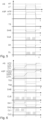
- Figure 3 shows communication waveforms over time t in an I2C system 1 for one slave 5 n on an I2C bus 7.
- the I2C bus system 1 is in an idle state. Neither a data bus signal DAB nor a clock bus signal CLB is provided.
- the addressing signal AS is a voltage signal.
- a signal conditioning circuit 14 may not include a voltage divider.
- a level of the processed addressing signal ASP is close to the addressing signal AS. This case is shown in Figure 3 . Both signals are zero or at any value below the low threshold value LT. Accordingly, the trigger signal TS is not provided and the switches 12, 13 are not enabled. Accordingly, also the data signal DA and the clock signal CL on the slave 5 n are not provided.
- a data package in the form of a data bus signal DAB and clock bus signal CLB intended for the slave 5 n is sent via the data bus line 8.
- the addressing signal AS and/or the processed addressing signal ASP is within the range [LT, HT] attributed to the slave 5 n .
- the trigger signal TS is provided to the switches 12, 13 and a data signal DA and clock signal CL is transmitted to the slave 5 n .
- the I2C system 1 return in its idle state, triggered by the addressing signal AS or the processed addressing signal ASP leaving the range [LT, HT] attributed to the slave 5 n .
- the switches 12, 13 are disabled and the slave 5 n is disconnected from the data bus 8 and clock bus 9.
- the I2C signals DAB, CLB are transferred to the slave 5 n only if the addressing signal AS or the processed addressing signal ASP is within the defined range [LT, HT].
- an addressing signal AS in the range of [LT1, HT1] is attributed.
- an addressing signal AS in the range of [LT2, HT2] is attributed.
- the signal ranges are non-overlapping ranges.
- a data package in the form of a data bus signal DAB and clock bus signal CLB intended for the first slave 5 1 is sent via the data bus 8. Accordingly, the signals are accompanied by an addressing signal AS, which after processing, corresponds to a processed addressing signal ASP with a value falling in the range [LT1, HT1].
- a trigger signal TS1 is sent to the switches 12, 13 of the first slave 5 1 and the data signal DAB and clock signal CLB is transferred as data signal DA1 and clock signal CL1 to the first slave 5 1 .
- the package has been transferred to the first slave 5 1 and the addressing signal AS or processed addressing signal ASP rises above the high threshold level HT1 for the first slave 5 1 .
- the processed addressing signal ASP is between the two ranges, the I2C bus system 1 is in the idle state.
- a data bus signal DAB and clock bus signal CLB intended for the second slave 5 2 is sent via the data bus line 8.
- the signals are accompanied by an addressing signal AS attributed to the second slave 5 2 .
- the addressing signal AS or processed addressing signal is within the range [LT2, HT2].
- the switches of the second slave 5 2 are enabled by the trigger signal TS2 and the data signal DAB and clock signal CLB is transferred as data signal DA2 and clock signal CL2 to the second slave 5 2 .
- the package has been transferred to the second slave 5 2 and the addressing signal AS or processed addressing signal ASP rises above the high threshold level HT2 for the second slave 5 2 .
- the bus system 1 is again in the idle state.
- Figure 5 shows communication waveforms over time t in an I2C system 1 for one slave 5 n on an I2C bus 7.
- This embodiment differs from the embodiment of Figure 3 in that the addressing signal AS is in the form of a current signal.
- the addressing signal AS is converted by the signal conditioning circuit 14 to a processed addressing signal ASP in the form of a voltage signal.
- the switches 12, 13 are enabled and the data package is transferred to the slave 5 n .
- the range for the processed addressing signal ASP corresponds to a range [LT, HT] for the addressing signal AS.
- Figure 6 shows communication waveforms over time t in an I2C system 1 for a first slave 5 1 and a second slave 5 2 on an I2C bus 7. Also here, this embodiment differs from the embodiment of Figure 4 in that the addressing signal AS is in the form of a current signal.
- a range [LT1, HT1] for the addressing signal AS in form of a current attributed to the first slave 5 1 corresponds to a range [LTP1, HTP1] of the processed addressing signal ASP in form of a voltage.
- a range [LT2, HT2] for the addressing signal AS in form of a current attributed to the second slave 5 2 corresponds to a range [LTP2, HTP2] of the processed addressing signal ASP in form of a voltage.
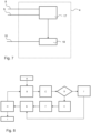
- FIG. 7 shows an embodiment of a master 4 in a schematic circuit diagram.
- the main part of the master 4 is a controller 17.
- the controller 17 may include a microcontroller, microprocessor, DSP, FPGA, CPLD, ASIC or SoC, for example.
- the controller 17 provides the data bus signal DAB and the clock bus signal CLB to the data bus 8 and clock bus 9. Furthermore, the controller 17 sets the signal level for the addressing signal AS and drives a D/A converter 18 which sends the respective addressing signal AS to the addressing signal line 10.
- the D/A converter 18 may provide either voltage or current.
- the D/A converter may include a discrete circuit and/or an integrated circuit. The D/A converter may be a part of the microcontroller, DSP, ASIC or SoC, for example.
- Figure 8 shows an embodiment of a control algorithm of a master 4.
- the algorithm for transmitting data via the I2C bus 7 to a specific slave 5 n starts in step A.
- the master 4, in particular the controller 17 checks in step B an internal look-up table in which for each slave 5 n the attributed level of the addressing signal AS is stored.
- the proper level of the addressing signal is set in step C, in particular by the D/A converter 18.
- step D it is checked if the particular slave 5 n is present on the I2C bus 7 by sending a small data package together with the addressing signal AS to the slave 5 n .
- step E the controller goes to the step E, where the communication with the slave 5 n is started.
- step J the controller 17 goes to the step J.
- step F data is read from or written on the slave memory 11.
- step G the communication with the slave memory 11 is stopped.
- step H the next slave 5 n is to be addressed and the algorithm steps are repeated.
- step I the level of the addressing signal AS is set to 0 V or 0 A and the I2C bus system 1 is set in the idle state.
- step J an error flag is set and then the controller 17 goes to the step G.
- Figures 9 to 11 show embodiments of setting a high threshold level HT and a low threshold level LT for a slave 5 n .
- the threshold levels HT and LT are set on the slave 5 n .
- Figure 9 shows setting a high threshold value HT by using a voltage divider 23 by providing two resistors R1 and R2.
- the high threshold value HT is the voltage that drops across one of the resistors R1, R2.
- the high threshold value is set as the voltage that drops across one of the further resistors R3, R4.
- the resistors R1, R2, R3, R4 can be provided on the slave 5 n .
- the resistors R1, R2, R3, R4 can be connected between ground (0V) and a voltage source +V.
- the resistors R1, R2, R3, R4 directly provide a coding for the respective slave 5 n .
- the resistance value of at least one of the resistors R1, R2, R3, R4 is different for different slaves 5 n . It is also possible that the number and/or electric connections of the resistors R1, R2, R3, R4 is different. Accordingly, the resistors R1, R2, R3, R4 have a double function of coding resistors Rx1, Rx2, Rx3, Rx4 and resistors of the voltage divider 23.
- the resistors R1, R2, R3 directly provide a coding for the respective slave 5 n .
- the resistors R1, R2, R3 have a double function as coding resistors Rx1, Rx2, Rx3 and resistors of the voltage divider 23.
- a programmable current source 19 is provided on the slave 5 n .
- the programmable current source 19 is connected in parallel to a coding resistor Rx.
- the coding is provided by the coding resistor Rx which is not part of the voltage divider 23. Accordingly, the resistance values of the coding resistors Rx are different for different slaves 5 n .
- Figures 12 to 14 show further embodiments of setting high and low threshold values HT, LT for a slave 5 n .
- the difference to the embodiments shown in Figures 9 to 11 is that capacitances C1, C2, C3, C4 are connected in parallel to the resistors R1, R2, R3.
- the capacitances C1, C2, C3, C4 are added for noise reduction.
- Figure 15 shows an embodiment of setting high and low threshold values for a slave 5 n externally. Accordingly, the threshold values are not set on the slave 5 n as in Figure 14 but on an external component such as the backplane 20.
- the threshold value may be set for each slot 2 n .
- the threshold value is set by a coding resistor Rx, wherein the resistance value can be set to a different value for each slot 2 n .
- capacitors C1, C2, C3 are present for noise reduction. It is also possible that the capacitors C1, C2, C3 are not provided.
- Figure 16 shows a further embodiment of setting high and low threshold values HT, LT for a slave 5 n externally.
- the resistance value is set by a coding circuit 21 for each slot 2 n .
- the coding circuit 21 is connected to the slave by a number N of coding signal lines.
- Each slot 2 n has a different coding so that each slot 2 n is identifiable.
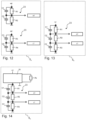
- FIG. 17A to 17c shows an embodiment of coding circuits 21, which may be used in the embodiments of Figure 16 , for example.
- coding circuits 21 are also present for the other slots.
- Each coding resistor Rx1-Rx5 can be connected or not connected to a specified voltage level +V on one side and to the associated slot 2 n on the other side.
- a coding resistor Rx1-Rx5 When a coding resistor Rx1-Rx5 is not connected to the specified voltage level +V it can be connected to ground (0V) or may be floating, for example.
- the specified voltage level +V is a level other than ground (0V) and can be positive.
- the specified voltage level +V may be a common voltage level for all resistors Rx1-Rx5 and all slots.
- coding resistors Rx1, Rx2, Rx4 are connected to the specified voltage level V, while coding resistors Rx3, Rx5 are connected to ground (0V) such that the binary coding corresponds to "0" "1" "0" "1" "1".
- each slot 2 n has the same layout of the coding circuit 21 but a different coding by a pattern of connecting and not connecting the coding resistors Rx1-Rx5 to the specified voltage +V.
- Figures 18A to 18C shows a further embodiment of coding circuits 21 for the slots 2 1 , 2 4 , 2 12 of an I2C system 1.
- the difference to the embodiment of Figures 17A to 17C is that coding resistors Rx1-Rx5 are only provided when being connected to the specified voltage +V, corresponding to the binary coding of "1".
- the coding signal lines N1-N5 which are not connected to a coding resistor Rx1-Rx5 are connected directly to ground (0V).
- each slot 2 1 , 2 4 , 2 12 has a different layout of the coding circuit 21.
- coding resistors Rx1-Rx5 only for a binary coding of "1" costs can be reduced.
- Figure 19 shows a further embodiment of setting high and low threshold values for a slot 2 n and associated slave 5 n externally.
- a coding resistor Rx is located on the backplane for each slot 2 n .
- a voltage source is used and the programmable current source is not present.
- capacitors C1, C2, C3 are present for noise reduction. It is also possible that the capacitors C1, C2, C3 are not provided.
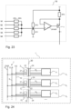
- Figures 20 and 21 show embodiments of a programmable current source 19.
- the programmable current source 19 may be used in the embodiments shown in Figures 11 , 14 or 15 , for example.
- the programmable current source 19 comprises two resistors RP1, RP2, an operational amplifier OPAMP and a transistor T (MOSFET, for example).
- the programmable current source 19 comprises a Zener diode DZ instead of the second resistor RP2.
- the programmable current source 19 comprises a voltage reference VREF instead of resistors RP1 and RP2.
- Figure 23 shows a further embodiment of a programmable current source 19.
- the programmable current source 19 may be used in the embodiment comprising a coding circuit as shown in Fig. 16 , Figs. 17A-17C and Figs. 18A-18C .
- the programmable current source comprises a third resistor RP3 instead of the connection to the outside coding resistor Rx of Fig. 20 and 21 .
- the coding signal lines N1-N5 are connected via further resistors RP4-RP8 to the coding circuit 21.
- Figure 24 shows a further embodiment of an I2C bus system 1 in a schematic circuit diagram.
- the coding circuit 21 is located on the backplane 20.
Landscapes
- Engineering & Computer Science (AREA)
- Theoretical Computer Science (AREA)
- General Engineering & Computer Science (AREA)
- Physics & Mathematics (AREA)
- General Physics & Mathematics (AREA)
- Computer Networks & Wireless Communication (AREA)
- Signal Processing (AREA)
- Computer Hardware Design (AREA)
- Dc Digital Transmission (AREA)
Abstract
Description
- The present disclosure relates to an I2C bus system. Such a system comprises several I2C slave devices which are to be connected to an I2C bus. The I2C devices may be EEPROM memory devices, for example. The I2C bus system may be a part of a rack-mounted I/O system comprising a backplane and a plurality of boards with various functions. The identification, configuration and calibration data for these boards can be stored in the EEPROM memory.
- Due to the I2C specification, the number of I2C slave devices to be connected to a common I2C bus is limited. In particular, it is not possible to connect more than one I2C slave device with the same I2C address to the common I2C bus. Commonly, eight different I2C slave addresses can be used with one type of EEPROM memory. In addition to that, the I2C specification defines the total capacity per I2C bus, which also limits the number of I2C slave devices on the same I2C bus.
-
US 6255973 B1 discloses an address selection circuitry, wherein addresses on an SM (System Management) bus are compared with a seven bit address stored in an address register.JP S59183551 A US 5673048 A discloses an analog voltage address decoder circuit and stackable voltage comparator circuit. - A few possible solutions have been found to enable addressing multiple slave devices. As an example, an addressable I2C bus switch can be provided on the I2C bus. However, in this case, the I2C master must be always connected at the same position on the I2C bus (the switch has dedicated pins for I2C master bus) and there may be the only one I2C slave with the same address per the I2C slave output. Moreover, this solution requires more complicated PCB design, due to many I2C connections. Another solution, comprising an I2C bus multiplexer, is similar to the solution with an I2C bus switch and presents the same disadvantages.
- Furthermore, an I2C address translator can be used, enabling the address of one or more I2C slave devices to be translated to a different address. However, also here, the position of the I2C master is fixed and this solution also requires a more complex PCB design. It is also possible to implement the required functionality in the design of digital logic devices such as an FPGA (Field-Programmable Gate Array) or a CPLD (Complex Programmable Logic device) or to use microcontrollers with at least two I2C controllers. However, both solutions are complex and expensive.
- Embodiments of the disclosure relate to an improved I2C bus system.
- According to a first aspect, an I2C bus system comprises a data bus, a clock bus and an addressing signal line for connecting a master and a plurality of slaves. The addressing signal line is configured to transmit an analog addressing signal from the master to the slaves. To each of the slaves, a range of the analog addressing signal or of a processed analog addressing signal is attributed, wherein the range is defined by a high threshold level and a low threshold level. The I2C bus system is configured to selectively connect each of the slaves to the data bus and clock bus only if the addressing signal is in the range.
- This allows connecting a plurality of slaves with the same I2C address to the I2C bus. At the same time, the master can be positioned in any slot on the backplane. It is also possible that all or some slaves have different I2C addresses. The master sets the level of the addressing signal sent over the addressing signal line to address a specific slave.
- The analog addressing signal may be transmitted to the slaves and processed in a signal conditioning circuit. The signal conditioning circuit may comprise a filter, in particular a low pass filter, a voltage divider and/or a protection circuit. The analog addressing signal may be a voltage signal or a current signal, for example. When the analog addressing signal is a current signal, the signal conditioning circuit may further comprise a current-to-voltage converter for converting the signal into a voltage signal. The specified range of the analog addressing signal may correspond to the same or a different specified range of the processed analog addressing signal.
- Each of the slaves may comprise a slave device connectable to and disconnectable from the I2C bus. The slave device may be a memory device, A/D converter, D/A converter, digital temperature sensor, I/O expander, digital power monitor and any other IC with I2C interface, for example.
- The I2C bus system may comprise at least one switch in the connection of the slave device with the I2C bus. In particular, each of the slaves may comprise a first switch in the connection of the slave device with the data bus and a second switch in the connection of the slave device with the clock bus.
- The switch may be enabled when the analog addressing signal is in the range attributed to the slave and disabled when the analog addressing signal is not within the range attributed to the slave. In the case of a mechanical switch, "enabled" means that the switch is closed and "disabled" means that the switch is open. Accordingly, the slave device is only connected to the I2C bus when the switch is enabled. A connection of the slave device to the I2C bus corresponds to the connection of the slave to the I2C bus.
- Each of the slaves may comprise a comparator for determining if the addressing signal is in the specified range. In particular, the comparator may compare the addressing signal with the high threshold level and low threshold level attributed to the slave.
- The attributed range may be coded on the slaves or externally. When the coding is provided externally, the coding may be provided on the backplane. In this case, a coding may be provided for each of the slots and for the backplane itself.
- For each of the slaves, the coding may be accomplished by one or more coding resistors. The coding resistors may be located on the slave or on the backplane. A voltage divider may set the high threshold level and the low threshold level based on the coding. A voltage divider may be located on each of the slaves. A voltage source or current source may be connected to the voltage divider.
- The coding may be directly accomplished by resistors of the voltage divider. In this case, the coding may be provided by different resistance values, numbers and/or electric connections of the resistors of the voltage divider on the slaves, for example.
- It is also possible that the coding is set by one or more coding resistors which are not part of the voltage divider. As an example, a voltage source may be connected to the voltage divider via the coding resistor. It is also possible that a programmable current source is provided wherein the coding resistor determines the current level. The coding resistor may have a different resistance value for the different slaves. The coding resistor may be located on the backplane or on the slave. When providing a separate coding resistor, the resistors of the voltage divider may have an identical layout for the different slaves.
- The coding of the slaves may be provided by a coding circuit for each slave. For at least one of the slaves, the coding circuit may comprise one or more coding resistors. The coding may be accomplished by a pattern of the coding resistors connected or not connected to a specific voltage level from one side. When the coding resistor is not connected to the specific voltage level it may be connected to ground (0V) or may be floating, for example. The coding circuit may be connected to the slave from the other side. It is also possible that one of the slaves is coded by not providing any coding resistors for this slave.
- For each slave, the coding resistors may be provided in the coding circuit and the coding may be accomplished by the connection or disconnection of the coding resistors to and from the specific voltage level. The coding resistors may have either the same or different resistance values. It is also possible that for each slave the coding circuit only comprises the coding resistors which are connected to the specific voltage level.
- According to a further aspect, a method for selectively connecting in an I2C bus system a plurality of slaves to a master comprises the steps of providing an I2C bus system comprising a master, a plurality of slaves, a data bus, a clock bus and an addressing line, attributing to each of the slaves a specified range of an analog addressing signal, the range being defined by a high threshold level and a low threshold level, sending a data bus signal on the data bus and a clock bus signal on the clock bus accompanied by an addressing signal on the addressing line and selectively connecting each of the slaves to the data bus and/or clock bus only if the addressing signal is in the attributed range.
- The I2C bus system in accordance with the method may have any structural and functional features of the I2C bus system in the foregoing.
- The present disclosure comprises several aspects and embodiments. Every feature described with respect to one of the aspects and embodiments is also disclosed herein with respect to the other aspects and embodiments, even if the respective feature is not explicitly mentioned in this context.
- Further features, refinements and expediencies become apparent from the following description of the exemplary embodiments in connection with the figures. In the figures, elements of the same structure and/or functionality may be referenced by the same reference signs. It is to be understood that the embodiments shown in the figures are illustrative representations and are not necessarily drawn to scale.
-
Figure 1 shows an embodiment of an I2C bus system in a schematic circuit diagram, -
Figure 2 shows an embodiment of a slave in a schematic circuit diagram, -
Figure 3 shows communication waveforms over time in an I2C system for one slave, -
Figure 4 shows communication waveforms over time in an I2C system for several slaves, -
Figure 5 shows communication waveforms over time in an I2C system for one slave with an addressing signal in the form of a voltage, -
Figure 6 shows communication waveforms over time in an I2C system for one slave with an addressing signal in the form of a current, -
Figure 7 shows an embodiment of a master in a schematic circuit diagram, -
Figure 8 shows an embodiment of a control algorithm of a master in a schematic circuit diagram, -
Figures 9 to 11 show embodiments of setting high and low threshold values on a slave, -
Figures 12 to 14 show further embodiments of setting high and low threshold values on a slave, -
Figure 15 shows an embodiment of setting high and low threshold values for a slave externally, -
Figure 16 shows a further embodiment of setting high and low threshold values for a slave externally, -
Figures 17A to 17C show an embodiment of coding circuits for different slots and the backplane, -
Figures 18A to 18C show a further embodiment of coding circuits for different slots and the backplane, -
Figure 19 shows a further embodiment of setting high and low threshold values for a slave externally, -
Figures 20 ,21 and 22 show embodiments of a programmable current source, -
Figures 23 shows a further embodiment of a programmable current source, -
Figure 24 shows a further embodiment of an I2C bus system. -
Figure 1 shows an embodiment of anI2C bus system 1. TheI2C bus system 1 is a part of an I/O (Input/Output) system, in particular a rack-mounted I/O system. In anI2C bus system 1, the I2C (Inter-integrated Circuit) communication protocol is used. AnI2C bus system 1 may be used in industrial automation and control systems, for example. TheI2C bus system 1 comprises a plurality ofslots boards - The plurality of
slots backplane connector 22. Thebackplane connector 22 is used for connection betweenI2C bus 7, located on the backplane, and a plurality ofslaves boards - The plurality of
boards board connector 24. Theboard connector 24 has the same functionality as thebackplane connector 22. Theboard connector 24 and thebackplane connector 22 are matched together. - The plurality of
boards master 4 and a plurality ofslaves master 4 and theslaves boards slot 2n and aboard 3n. Accordingly, in each of theslots 2n, aboard 3n comprising amaster 4 or aslave 5n containing the configuration memory perslot 2n can be inserted. - The
master 4 andslaves 5n are connected to acommon I2C bus 7 comprising adata bus 8 and a clock bus 9. Thedata bus 8 is the signal line for transmitting data in a bidirectional manner (SDA). A data bus signal DAB is transmitted on thedata bus 8. The clock bus 9 is the signal line for clock synchronization (SCL). A clock bus signal CLB is transmitted on the clock bus 9. - Typically, racks with 10 or 21
slots 2n are provided. If a configuration memory perslot 2n is used and one configuration memory is used on the backplane, then up to 11 or 22 memories are to be connected to thesingle I2C bus 7. However, a typical I2C memory can be configured with only up to eight different slave addresses. It is usually not possible to connect two memories with the same address and more than eight memories to the one I2C bus. Furthermore, the I2C bus specification limits the total capacity per I2C bus. - The
I2C bus system 1 comprises in addition to theI2C bus 7 an addressingsignal line 10 which makes it possible to connect memories with the same I2C address to thecommon I2C bus 7. Accordingly, each of themaster 4 andslaves I2C bus 7 but also to the addressingsignal line 10. The addressingsignal line 10 provides an analog addressing signal AS so that also memories having the same I2C addresses can be connected to thecommon I2C bus 7. - To each slave 5n a specified range of the analog addressing signal AS is attributed. The specified ranges for the
different slaves 5n are non-overlapping. Accordingly, the analog addressing signal AS is unique for eachslave 5n. - The
slaves 5n may have the same I2C address. It is also possible that theslaves 5n have different I2C addresses. In both cases, a specified range of the addressing signal AS can be attributed to each of theslaves 5n. - The
I2C bus system 1 is flexible, as themaster 4 can be connected to any place on theI2C bus 7, i.e., can be inserted in any of theslots - Generally, in the figures, pull-up resistors for the
data bus 8 and clock bus 9 are not shown but may be provided. -
Figure 2 shows aslave 5n comprising aslave device 11. Theslave device 11 may be a memory device. Theslave 5n may be one of theslaves 5n shown inFigure 1 . - The
slave device 11 is connected to thedata bus 8 via afirst switch 12 and to the clock bus 9 via asecond switch 13. Theswitches specific slave 5n, theswitches slave device 11 is connected to thedata bus 8 and the clock bus 9. Thefirst switch 12 andsecond switch 13 may be integrated in the same switch component, for example different ports of a switch, or may be separate switch components. - The
switches - The addressing signal AS is provided to a signal conditioning circuit 14, which may comprise a voltage divider, a low pass filter and/or a protection circuit. The addressing signal AS may be in the form of a voltage or current signal. The processed addressing signal ASP is provided to a
comparator 15 which compares the processed addressing signal ASP to a high threshold level HT and a low threshold level LT and determines if the processed addressing signal ASP is within the attributed range [LT,HT]. - The
comparator 15 may be a window comparator circuit. In particular, the processed addressing signal ASP may be an input voltage VIN to thecomparator 15 and the threshold levels HT, LT may be threshold voltages VTH+ and VTH-. The trigger signal TS may be in the form of an output voltage VOUT. The threshold levels HT, LT can be set by one or more coding resistors which may be on theslave 5n or on thebackplane 20. Each of the coding resistors may be a single resistor or a combination of resistors connected in series or a combination of resistors connected in parallel or a combination of the resistors connected in combination of the series and parallel resistors, for example. Generally, the trigger signal TS may be an analog or digital signal. - In the default state, the addressing signal AS and processed addressing signal ASP is equal to zero and the
I2C bus system 1 will be in an idle state. Accordingly, theswitches slave devices 11 and theI2C bus 7 is not loaded with any of theslave devices 11. If the processed addressing signal ASP is within the range attributed to aspecific slave 5n, a trigger signal TS is sent to theswitches trigger signal line 16 and theswitches data bus 8 and clock bus 9 are connected to theslave device 11. - When the analog addressing signal AS is a current signal, the signal conditioning circuit 14 comprises a current-to-voltage converter for converting the input signal to a voltage. Also in this case, the signal conditioning circuit 14 may further comprise a low pass filter, a voltage divider and/or a protection circuit. In the default state, the current is equal to zero and the system is in an idle state. When the current level is within a range determined by a low and high current threshold, which corresponds to low and high voltage thresholds of the
comparator 15, thecomparator 15 sends the trigger signal TS to enable theswitches - The trigger signal TS can be either analog or digital (HIGH or LOW logic state). When the
switches slave 5n is enabled. - When the level of the addressing signal AS is out of the range defined by the low threshold level LT and high threshold level HT, the
slave 5n and, in particular, theslave device 11 is disconnected from theI2C bus 7. - With the connection and disconnection of the
slaves 5n from theI2C bus 7, the I2C bus specification, which limits the total capacity per I2C bus, can be complied with, also when a high number ofslaves 5n are present. - Furthermore, the
I2C bus system 1 does not limit the position of themaster 4. Accordingly, it is possible to position themaster 4 in eachslot I2C bus system 1. -
Figure 3 shows communication waveforms over time t in anI2C system 1 for oneslave 5n on anI2C bus 7. - At the beginning, the
I2C bus system 1 is in an idle state. Neither a data bus signal DAB nor a clock bus signal CLB is provided. The addressing signal AS is a voltage signal. When the addressing signal level AS is not higher than a voltage level of +V then a signal conditioning circuit 14 may not include a voltage divider. Then a level of the processed addressing signal ASP is close to the addressing signal AS. This case is shown inFigure 3 . Both signals are zero or at any value below the low threshold value LT. Accordingly, the trigger signal TS is not provided and theswitches slave 5n are not provided. - At a first time t1, a data package in the form of a data bus signal DAB and clock bus signal CLB intended for the
slave 5n is sent via thedata bus line 8. The addressing signal AS and/or the processed addressing signal ASP is within the range [LT, HT] attributed to theslave 5n. Thus, the trigger signal TS is provided to theswitches slave 5n. - At a later second time t2, the
I2C system 1 return in its idle state, triggered by the addressing signal AS or the processed addressing signal ASP leaving the range [LT, HT] attributed to theslave 5n. Theswitches slave 5n is disconnected from thedata bus 8 and clock bus 9. - Accordingly, the I2C signals DAB, CLB are transferred to the
slave 5n only if the addressing signal AS or the processed addressing signal ASP is within the defined range [LT, HT]. -
Figure 4 shows communication waveforms over time t in anI2C system 1 for afirst slave 51 and asecond slave 52 on anI2C bus 7. Similar toFigure 3 , the waveforms show a case when a voltage divider is not included in a signal conditioning circuit 14. - To the
first slave 51, an addressing signal AS in the range of [LT1, HT1] is attributed. For thesecond slave 52, an addressing signal AS in the range of [LT2, HT2] is attributed. The signal ranges are non-overlapping ranges. - At a first time t1, a data package in the form of a data bus signal DAB and clock bus signal CLB intended for the
first slave 51 is sent via thedata bus 8. Accordingly, the signals are accompanied by an addressing signal AS, which after processing, corresponds to a processed addressing signal ASP with a value falling in the range [LT1, HT1]. Thus, a trigger signal TS1 is sent to theswitches first slave 51 and the data signal DAB and clock signal CLB is transferred as data signal DA1 and clock signal CL1 to thefirst slave 51. - At a second time t2, the package has been transferred to the
first slave 51 and the addressing signal AS or processed addressing signal ASP rises above the high threshold level HT1 for thefirst slave 51. When the processed addressing signal ASP is between the two ranges, theI2C bus system 1 is in the idle state. - At a third time t3, a data bus signal DAB and clock bus signal CLB intended for the
second slave 52 is sent via thedata bus line 8. The signals are accompanied by an addressing signal AS attributed to thesecond slave 52. Accordingly, the addressing signal AS or processed addressing signal is within the range [LT2, HT2]. The switches of thesecond slave 52 are enabled by the trigger signal TS2 and the data signal DAB and clock signal CLB is transferred as data signal DA2 and clock signal CL2 to thesecond slave 52. - At a fourth time t4, the package has been transferred to the
second slave 52 and the addressing signal AS or processed addressing signal ASP rises above the high threshold level HT2 for thesecond slave 52. Thebus system 1 is again in the idle state. -
Figure 5 shows communication waveforms over time t in anI2C system 1 for oneslave 5n on anI2C bus 7. This embodiment differs from the embodiment ofFigure 3 in that the addressing signal AS is in the form of a current signal. The addressing signal AS is converted by the signal conditioning circuit 14 to a processed addressing signal ASP in the form of a voltage signal. - When the processed addressing signal ASP is in a range [LTP, HTP] attributed to a
slave 5n, theswitches slave 5n. The range for the processed addressing signal ASP corresponds to a range [LT, HT] for the addressing signal AS. -
Figure 6 shows communication waveforms over time t in anI2C system 1 for afirst slave 51 and asecond slave 52 on anI2C bus 7. Also here, this embodiment differs from the embodiment ofFigure 4 in that the addressing signal AS is in the form of a current signal. - Like in
Figure 5 , a range [LT1, HT1] for the addressing signal AS in form of a current attributed to thefirst slave 51 corresponds to a range [LTP1, HTP1] of the processed addressing signal ASP in form of a voltage. A range [LT2, HT2] for the addressing signal AS in form of a current attributed to thesecond slave 52 corresponds to a range [LTP2, HTP2] of the processed addressing signal ASP in form of a voltage. -
Figure 7 shows an embodiment of amaster 4 in a schematic circuit diagram. The main part of themaster 4 is acontroller 17. Thecontroller 17 may include a microcontroller, microprocessor, DSP, FPGA, CPLD, ASIC or SoC, for example. - The
controller 17 provides the data bus signal DAB and the clock bus signal CLB to thedata bus 8 and clock bus 9. Furthermore, thecontroller 17 sets the signal level for the addressing signal AS and drives a D/A converter 18 which sends the respective addressing signal AS to the addressingsignal line 10. The D/A converter 18 may provide either voltage or current. The D/A converter may include a discrete circuit and/or an integrated circuit. The D/A converter may be a part of the microcontroller, DSP, ASIC or SoC, for example. -
Figure 8 shows an embodiment of a control algorithm of amaster 4. The algorithm for transmitting data via theI2C bus 7 to aspecific slave 5n starts in step A. - The
master 4, in particular thecontroller 17 checks in step B an internal look-up table in which for eachslave 5n the attributed level of the addressing signal AS is stored. The proper level of the addressing signal is set in step C, in particular by the D/A converter 18. In step D, it is checked if theparticular slave 5n is present on theI2C bus 7 by sending a small data package together with the addressing signal AS to theslave 5n. - When the check has been successful, the controller goes to the step E, where the communication with the
slave 5n is started. When the check has not been successful, thecontroller 17 goes to the step J. In step F, data is read from or written on theslave memory 11. - In step G, the communication with the
slave memory 11 is stopped. In step H, thenext slave 5n is to be addressed and the algorithm steps are repeated. - Alternatively, the communication on the
I2C bus 7 is stopped. In this case, in step I, the level of the addressing signal AS is set to 0 V or 0 A and theI2C bus system 1 is set in the idle state. - In step J, an error flag is set and then the
controller 17 goes to the step G. -
Figures 9 to 11 show embodiments of setting a high threshold level HT and a low threshold level LT for aslave 5n. In these embodiments, the threshold levels HT and LT are set on theslave 5n. -
Figure 9 shows setting a high threshold value HT by using avoltage divider 23 by providing two resistors R1 and R2. The high threshold value HT is the voltage that drops across one of the resistors R1, R2. In the same way, the high threshold value is set as the voltage that drops across one of the further resistors R3, R4. - The resistors R1, R2, R3, R4 can be provided on the
slave 5n. The resistors R1, R2, R3, R4 can be connected between ground (0V) and a voltage source +V. - In this case, the resistors R1, R2, R3, R4 directly provide a coding for the
respective slave 5n. As an example, the resistance value of at least one of the resistors R1, R2, R3, R4 is different fordifferent slaves 5n. It is also possible that the number and/or electric connections of the resistors R1, R2, R3, R4 is different. Accordingly, the resistors R1, R2, R3, R4 have a double function of coding resistors Rx1, Rx2, Rx3, Rx4 and resistors of thevoltage divider 23. - In
Figure 10 , the high threshold level HT and the low threshold level LT are set by avoltage divider 23 by providing three resistors R1, R2, R3 connected in series. - Also here, the resistors R1, R2, R3 directly provide a coding for the
respective slave 5n. In this example, the resistors R1, R2, R3 have a double function as coding resistors Rx1, Rx2, Rx3 and resistors of thevoltage divider 23. - In
Figure 11 , a programmablecurrent source 19 is provided on theslave 5n. The programmablecurrent source 19 is connected in parallel to a coding resistor Rx. - In this case, the coding is provided by the coding resistor Rx which is not part of the
voltage divider 23. Accordingly, the resistance values of the coding resistors Rx are different fordifferent slaves 5n. -
Figures 12 to 14 show further embodiments of setting high and low threshold values HT, LT for aslave 5n. The difference to the embodiments shown inFigures 9 to 11 is that capacitances C1, C2, C3, C4 are connected in parallel to the resistors R1, R2, R3. The capacitances C1, C2, C3, C4 are added for noise reduction. -
Figure 15 shows an embodiment of setting high and low threshold values for aslave 5n externally. Accordingly, the threshold values are not set on theslave 5n as inFigure 14 but on an external component such as thebackplane 20. - The threshold value may be set for each
slot 2n. The threshold value is set by a coding resistor Rx, wherein the resistance value can be set to a different value for eachslot 2n. - Also here, the capacitors C1, C2, C3 are present for noise reduction. It is also possible that the capacitors C1, C2, C3 are not provided.
-
Figure 16 shows a further embodiment of setting high and low threshold values HT, LT for aslave 5n externally. In this case, the resistance value is set by acoding circuit 21 for eachslot 2n. Thecoding circuit 21 is connected to the slave by a number N of coding signal lines. Eachslot 2n has a different coding so that eachslot 2n is identifiable. -
Figures 17A to 17c shows an embodiment ofcoding circuits 21, which may be used in the embodiments ofFigure 16 , for example. In the figures, only thefirst slot 21, thefourth slot 24 and thetwelfth slot 212 are shown. However, thecoding circuits 21 are also present for the other slots. - Each coding resistor Rx1-Rx5 can be connected or not connected to a specified voltage level +V on one side and to the associated
slot 2n on the other side. When a coding resistor Rx1-Rx5 is not connected to the specified voltage level +V it can be connected to ground (0V) or may be floating, for example. The specified voltage level +V is a level other than ground (0V) and can be positive. The specified voltage level +V may be a common voltage level for all resistors Rx1-Rx5 and all slots. - For the
first slot 21, none of the coding resistors Rx1-Rx5 is connected to the specified voltage level such that the binary coding corresponds to "0" "0" "0" "0" "0". For thefourth slot 24, coding resistors Rx1, Rx2 are connected to the specified voltage level while coding resistors Rx3, Rx4, Rx5 are connected to ground. The binary coding corresponds to "0" "0" "0" "1" "1". For thetwelfth slot 212, coding resistors Rx1, Rx2, Rx4 are connected to the specified voltage level V, while coding resistors Rx3, Rx5 are connected to ground (0V) such that the binary coding corresponds to "0" "1" "0" "1" "1". - Accordingly, in this case, each
slot 2n has the same layout of thecoding circuit 21 but a different coding by a pattern of connecting and not connecting the coding resistors Rx1-Rx5 to the specified voltage +V. -
Figures 18A to 18C shows a further embodiment ofcoding circuits 21 for theslots I2C system 1. The difference to the embodiment ofFigures 17A to 17C is that coding resistors Rx1-Rx5 are only provided when being connected to the specified voltage +V, corresponding to the binary coding of "1". The coding signal lines N1-N5 which are not connected to a coding resistor Rx1-Rx5 are connected directly to ground (0V). - Accordingly, in this case, each
slot coding circuit 21. By providing coding resistors Rx1-Rx5 only for a binary coding of "1", costs can be reduced. -
Figure 19 shows a further embodiment of setting high and low threshold values for aslot 2n and associatedslave 5n externally. As inFigure 15 , a coding resistor Rx is located on the backplane for eachslot 2n. However, here, a voltage source is used and the programmable current source is not present. - Also here, the capacitors C1, C2, C3 are present for noise reduction. It is also possible that the capacitors C1, C2, C3 are not provided.
-
Figures 20 and21 show embodiments of a programmablecurrent source 19. The programmablecurrent source 19 may be used in the embodiments shown inFigures 11 ,14 or15 , for example. - In the embodiment of
Fig. 20 , the programmablecurrent source 19 comprises two resistors RP1, RP2, an operational amplifier OPAMP and a transistor T (MOSFET, for example). In the embodiment ofFig. 21 , the programmablecurrent source 19 comprises a Zener diode DZ instead of the second resistor RP2. In the embodiment ofFig. 22 , the programmablecurrent source 19 comprises a voltage reference VREF instead of resistors RP1 and RP2. -
Figure 23 shows a further embodiment of a programmablecurrent source 19. The programmablecurrent source 19 may be used in the embodiment comprising a coding circuit as shown inFig. 16 ,Figs. 17A-17C and Figs. 18A-18C . - The programmable current source comprises a third resistor RP3 instead of the connection to the outside coding resistor Rx of
Fig. 20 and21 . The coding signal lines N1-N5 are connected via further resistors RP4-RP8 to thecoding circuit 21. -
Figure 24 shows a further embodiment of anI2C bus system 1 in a schematic circuit diagram. Thecoding circuit 21 is located on thebackplane 20. -
- 1
- I2C bus system
- 21
- first slot
- 22
- second slot
- 24
- fourth slot
- 212
- twelfth slot
- 2n
- n-th slot
- 31
- first board
- 32
- second board
- 33
- third
- 3,
- n-th board
- 4
- master
- 51
- first slave
- 52
- second slave
- 54
- fourth slave
- 512
- twelfth slave
- 5n
- n-th slave
- 7
- I2C bus
- 8
- data bus
- 9
- clock bus
- 10
- addressing signal line
- 11
- slave device
- 12
- first switch
- 13
- second switch
- 14
- signal conditioning circuit
- 15
- comparator
- 16
- trigger signal line
- 17
- controller
- 18
- D/A converter
- 19
- programmable current source
- 20
- backplane
- 21
- coding circuit
- 22
- backplane connector
- 23
- voltage divider
- 24
- board connector
- +V
- voltage source
- I
- current
- V
- voltage
- VREF
- voltage reference
- AS
- (VA/IA) analog addressing signal
- ASP
- (VI) processed addressing signal
- CLB
- clock bus signal
- DAB
- data bus signal
- OPAMP
- operational amplifier
- T
- transistor
- TS
- trigger signal
- TS1
- trigger signal on first slave
- TS2
- trigger signal on second slave
- DA
- data signal on slave
- DA1
- data signal on first slave
- DA2
- data signal on second slave
- CL
- clock signal on slave
- CL1
- clock signal on first slave
- CL2
- clock signal on second slave
- HT
- high threshold level
- HT1
- high threshold level for first slave
- HT2
- high threshold level for second slave
- LT
- low threshold level
- LT1
- low threshold level for first slave
- LT2
- low threshold level for second slave
- HTP
- high threshold level for processed signal
- HTP1
- high threshold level for processed signal for first slave
- HTP2
- high threshold level for processed signal for second slave
- LTP
- low threshold level for processed signal
- LTP1
- low threshold level for processed signal for first slave
- LTP2
- low threshold level for processed signal for second slave
- R1, R2, R3, R4
- resistors in voltage divider
- Rx, Rx1-Rx5
- coding resistors
- RP1-RP8
- resistors in programmable current source
Claims (15)
- An I2C bus system (1),comprising a data bus (8), a clock bus (9) and an addressing signal line (10) for connecting a master (4) and a plurality of slaves (5n),wherein the addressing signal line (10) is configured to transmit an analog addressing signal (AS) from the master (4) to the slaves (5n),wherein to each of the slaves (5n) a range of the analog addressing signal (AS) and or a processed analog addressing signal (ASP) is attributed, the range being defined by a high threshold level (HT) and a low threshold level (LT),wherein the I2C bus system (1) is configured to selectively connect each of the slaves (5n) to the data bus (8) and clock bus (9) only if the addressing signal is in the range.
- The I2C bus system (1) of claim 1,
wherein each of the slaves (5n) comprises a slave device (11) and at least one switch (12, 13) in the connection of the slave device (11) with the I2C bus (7). - The I2C bus system (1) of claim 2,
wherein the switch (5, 6) is enabled when the analog addressing signal is in the range attributed to the slave (5n) and disabled when the analog addressing signal (AS) is not within the range attributed to the slave (5n). - The I2C bus system (1) of any of claims 2 or 3,
wherein each of the slaves (5n) comprises a first switch (11) in the connection with the data bus (8) and a second switch (13) in the connection with the clock bus (9). - The I2C bus system (1) of any of the preceding claims, wherein the master (4) is configured to set a level of the addressing signal (AS).
- The I2C bus system (1) of any of the preceding claims, wherein the analog addressing signal (AS) is a voltage or current signal.
- The I2C bus system (1) of any of the preceding claims, wherein each of the slaves (5n) comprises a comparator (15) for determining if the addressing signal (AS) is in the range.
- The I2C bus system (1) of any of the preceding claims, wherein the range is coded on each of the slaves (5n) or on a backplane (20) of the I2C bus system (1).
- The I2C bus system (1) of any of the preceding claims, wherein at least one coding resistor (Rx, Rx1-Rx5) determining the range is located on at least one of the slaves (5n) or on a backplane (20) of the I2C bus system (1).
- The I2C bus system (1) of any of the preceding claims, comprising at least one voltage divider (23) for setting the low threshold level (LT) and the high threshold level (HT).
- The I2C bus system (1) of claim 10,
wherein the coding of the slaves (5n) is accomplished by at one or more coding resistors (Rx, Rx1-Rx5) which are not part of the voltage divider (23). - The I2C bus system (1) of any of the preceding claims, wherein the range is coded by a coding circuit (21) comprising one or more coding resistors (Rx, Rx1-Rx5), wherein the coding is accomplished by a pattern of the coding resistors (Rx, Rx1-Rx5) connected or not connected to a specific voltage level (+V) from one side and connected to the slave (5n) from the other side.
- The I2C bus system (1) of claim 12,
wherein for each slave (5n) coding resistors (Rx, Rx1-Rx5) of the same number and values are provided in the coding circuit (21) and the coding is accomplished by the connection of the coding resistors (Rx, Rx1-Rx5) to a specific voltage level (+V) on one side or wherein for each slave (5n) the coding circuit (21) only comprises the coding resistors (Rx, Rx1-Rx5) which are connected to a specific voltage level (+V) on one side. - The I2C bus system (1) of claim 10,
wherein the range is coded on each of the slaves (5n), wherein the coding of the slaves (5n) is accomplished by the resistors (R1, R2, R3, R4) of the voltage divider (23). - A method for selectively connecting in an I2C bus system (1) a plurality of slaves (5n) to a master (4),comprising the steps of providing an I2C bus system (1) comprising a master (4), a plurality of slaves (5n), a data bus (8), a clock bus (9) and an addressing signal line (10), attributing to each of the slaves (5n) a range of an analog addressing signal (AS), the range being defined by a high threshold level (HT) and a low threshold level (LT),sending a data bus signal (DAB) on the data bus (8) and a clock bus signal (CLB) on the clock bus (9) accompanied by an addressing signal (AS) on the addressing signal line (10) and selectively connecting each of the slaves (5n) to the data bus (8) and/or clock bus (9) only if the addressing signal (AS) is in the range.
Priority Applications (1)
| Application Number | Priority Date | Filing Date | Title |
|---|---|---|---|
| EP23213333.0A EP4564183A1 (en) | 2023-11-30 | 2023-11-30 | I2c bus system and method for selectively connecting in an i2c bus system a plurality of slaves to a master |
Applications Claiming Priority (1)
| Application Number | Priority Date | Filing Date | Title |
|---|---|---|---|
| EP23213333.0A EP4564183A1 (en) | 2023-11-30 | 2023-11-30 | I2c bus system and method for selectively connecting in an i2c bus system a plurality of slaves to a master |
Publications (1)
| Publication Number | Publication Date |
|---|---|
| EP4564183A1 true EP4564183A1 (en) | 2025-06-04 |
Family
ID=89030023
Family Applications (1)
| Application Number | Title | Priority Date | Filing Date |
|---|---|---|---|
| EP23213333.0A Pending EP4564183A1 (en) | 2023-11-30 | 2023-11-30 | I2c bus system and method for selectively connecting in an i2c bus system a plurality of slaves to a master |
Country Status (1)
| Country | Link |
|---|---|
| EP (1) | EP4564183A1 (en) |
Cited By (2)
| Publication number | Priority date | Publication date | Assignee | Title |
|---|---|---|---|---|
| CN120448323A (en) * | 2025-07-10 | 2025-08-08 | 安徽大学 | A method and system for improving I2C bus read and write efficiency and reliability |
| CN120523758A (en) * | 2025-07-23 | 2025-08-22 | 苏州元脑智能科技有限公司 | Control device and control method |
Citations (6)
| Publication number | Priority date | Publication date | Assignee | Title |
|---|---|---|---|---|
| JPS59183551A (en) | 1983-04-01 | 1984-10-18 | Nec Corp | Address selecting circuit |
| US5673048A (en) | 1995-04-14 | 1997-09-30 | Delco Electronics Corporation | Analog voltage address decoder circuit |
| US6255973B1 (en) | 1999-08-26 | 2001-07-03 | Analog Devices, Inc. | Address selection circuitry and method using single analog input line |
| WO2009142632A1 (en) * | 2008-05-21 | 2009-11-26 | Hewlett-Packard Development Company, L.P. | Multi-drop serial bus with location detection and method |
| EP2778941A1 (en) * | 2013-03-14 | 2014-09-17 | Linear Technology Corporation | Address translation in I2C data communications system |
| EP3092573A1 (en) * | 2014-10-17 | 2016-11-16 | Lexmark International, Inc. | Methods for setting the address of a module |
-
2023
- 2023-11-30 EP EP23213333.0A patent/EP4564183A1/en active Pending
Patent Citations (6)
| Publication number | Priority date | Publication date | Assignee | Title |
|---|---|---|---|---|
| JPS59183551A (en) | 1983-04-01 | 1984-10-18 | Nec Corp | Address selecting circuit |
| US5673048A (en) | 1995-04-14 | 1997-09-30 | Delco Electronics Corporation | Analog voltage address decoder circuit |
| US6255973B1 (en) | 1999-08-26 | 2001-07-03 | Analog Devices, Inc. | Address selection circuitry and method using single analog input line |
| WO2009142632A1 (en) * | 2008-05-21 | 2009-11-26 | Hewlett-Packard Development Company, L.P. | Multi-drop serial bus with location detection and method |
| EP2778941A1 (en) * | 2013-03-14 | 2014-09-17 | Linear Technology Corporation | Address translation in I2C data communications system |
| EP3092573A1 (en) * | 2014-10-17 | 2016-11-16 | Lexmark International, Inc. | Methods for setting the address of a module |
Cited By (3)
| Publication number | Priority date | Publication date | Assignee | Title |
|---|---|---|---|---|
| CN120448323A (en) * | 2025-07-10 | 2025-08-08 | 安徽大学 | A method and system for improving I2C bus read and write efficiency and reliability |
| CN120448323B (en) * | 2025-07-10 | 2025-09-30 | 安徽大学 | A method and system for improving I2C bus read and write efficiency and reliability |
| CN120523758A (en) * | 2025-07-23 | 2025-08-22 | 苏州元脑智能科技有限公司 | Control device and control method |
Similar Documents
| Publication | Publication Date | Title |
|---|---|---|
| EP4564183A1 (en) | I2c bus system and method for selectively connecting in an i2c bus system a plurality of slaves to a master | |
| US6690191B2 (en) | Bi-directional output buffer | |
| Leens | An introduction to I 2 C and SPI protocols | |
| EP2899556B1 (en) | Semiconductor device and battery voltage monitoring device | |
| US12003346B2 (en) | System and method for dual-port communication and power delivery | |
| EP3092575B1 (en) | Methods and apparatus for setting the address of a module using a clock | |
| CN109509422B (en) | Display panel drive circuit and display device | |
| US9448960B2 (en) | Address translation in I2C data communications system | |
| US10817452B2 (en) | Bus system and detection method thereof | |
| US8230151B2 (en) | Configurable data port for I2C or single-wire broadcast interface | |
| US6255973B1 (en) | Address selection circuitry and method using single analog input line | |
| US20090119439A1 (en) | Structure compatible with i2c bus and system management bus and timing buffering apparatus thereof | |
| CN112148656B (en) | Communication system and method for communication between a host device and a plurality of slave devices | |
| WO2008005112A2 (en) | Configurable voltage regulator | |
| EP1869563B1 (en) | Configurable data port for i2c or single-wire broadcast interface | |
| US6777975B1 (en) | Input-output bus interface to bridge different process technologies | |
| US20100013539A1 (en) | Communication circuit with selectable signal voltage | |
| CN112953221A (en) | Voltage conversion device | |
| CN112115088B (en) | Integrated circuit and method for assigning addresses to a plurality of slave devices | |
| KR101023280B1 (en) | Data communication systems | |
| US20080091788A1 (en) | Controller, address control method, and data transmission system using the same | |
| JP2024176021A (en) | Data Processing Unit | |
| WO2026094488A1 (en) | Serial communication system | |
| EP4151958A1 (en) | Sensing system comprising a chain of sensors | |
| JP2025098355A (en) | Semiconductor device and communication system |
Legal Events
| Date | Code | Title | Description |
|---|---|---|---|
| PUAI | Public reference made under article 153(3) epc to a published international application that has entered the european phase |
Free format text: ORIGINAL CODE: 0009012 |
|
| STAA | Information on the status of an ep patent application or granted ep patent |
Free format text: STATUS: THE APPLICATION HAS BEEN PUBLISHED |
|
| AK | Designated contracting states |
Kind code of ref document: A1 Designated state(s): AL AT BE BG CH CY CZ DE DK EE ES FI FR GB GR HR HU IE IS IT LI LT LU LV MC ME MK MT NL NO PL PT RO RS SE SI SK SM TR |
|
| STAA | Information on the status of an ep patent application or granted ep patent |
Free format text: STATUS: REQUEST FOR EXAMINATION WAS MADE |
|
| 17P | Request for examination filed |
Effective date: 20251204 |
|
| GRAP | Despatch of communication of intention to grant a patent |
Free format text: ORIGINAL CODE: EPIDOSNIGR1 |
|
| STAA | Information on the status of an ep patent application or granted ep patent |
Free format text: STATUS: GRANT OF PATENT IS INTENDED |