EP4564404A1 - Verfahren zur entfernung von rückständen von einer substratoberfläche - Google Patents
Verfahren zur entfernung von rückständen von einer substratoberfläche Download PDFInfo
- Publication number
- EP4564404A1 EP4564404A1 EP23213742.2A EP23213742A EP4564404A1 EP 4564404 A1 EP4564404 A1 EP 4564404A1 EP 23213742 A EP23213742 A EP 23213742A EP 4564404 A1 EP4564404 A1 EP 4564404A1
- Authority
- EP
- European Patent Office
- Prior art keywords
- layer
- substrate
- auxiliary layer
- temporary
- bonding
- Prior art date
- Legal status (The legal status is an assumption and is not a legal conclusion. Google has not performed a legal analysis and makes no representation as to the accuracy of the status listed.)
- Withdrawn
Links
Images



Classifications
-
- H—ELECTRICITY
- H10—SEMICONDUCTOR DEVICES; ELECTRIC SOLID-STATE DEVICES NOT OTHERWISE PROVIDED FOR
- H10P—GENERIC PROCESSES OR APPARATUS FOR THE MANUFACTURE OR TREATMENT OF DEVICES COVERED BY CLASS H10
- H10P50/00—Etching of wafers, substrates or parts of devices
- H10P50/20—Dry etching; Plasma etching; Reactive-ion etching
- H10P50/28—Dry etching; Plasma etching; Reactive-ion etching of insulating materials
- H10P50/282—Dry etching; Plasma etching; Reactive-ion etching of insulating materials of inorganic materials
- H10P50/283—Dry etching; Plasma etching; Reactive-ion etching of insulating materials of inorganic materials by chemical means
-
- H—ELECTRICITY
- H10—SEMICONDUCTOR DEVICES; ELECTRIC SOLID-STATE DEVICES NOT OTHERWISE PROVIDED FOR
- H10P—GENERIC PROCESSES OR APPARATUS FOR THE MANUFACTURE OR TREATMENT OF DEVICES COVERED BY CLASS H10
- H10P14/00—Formation of materials, e.g. in the shape of layers or pillars
- H10P14/60—Formation of materials, e.g. in the shape of layers or pillars of insulating materials
- H10P14/68—Organic materials, e.g. photoresists
- H10P14/683—Organic materials, e.g. photoresists carbon-based polymeric organic materials, e.g. polyimides, poly cyclobutene or PVC
-
- H—ELECTRICITY
- H10—SEMICONDUCTOR DEVICES; ELECTRIC SOLID-STATE DEVICES NOT OTHERWISE PROVIDED FOR
- H10P—GENERIC PROCESSES OR APPARATUS FOR THE MANUFACTURE OR TREATMENT OF DEVICES COVERED BY CLASS H10
- H10P14/00—Formation of materials, e.g. in the shape of layers or pillars
- H10P14/60—Formation of materials, e.g. in the shape of layers or pillars of insulating materials
- H10P14/69—Inorganic materials
- H10P14/6903—Inorganic materials containing silicon
- H10P14/6905—Inorganic materials containing silicon being a silicon carbide or silicon carbonitride and not containing oxygen, e.g. SiC or SiC:H
-
- H—ELECTRICITY
- H10—SEMICONDUCTOR DEVICES; ELECTRIC SOLID-STATE DEVICES NOT OTHERWISE PROVIDED FOR
- H10P—GENERIC PROCESSES OR APPARATUS FOR THE MANUFACTURE OR TREATMENT OF DEVICES COVERED BY CLASS H10
- H10P50/00—Etching of wafers, substrates or parts of devices
- H10P50/20—Dry etching; Plasma etching; Reactive-ion etching
- H10P50/28—Dry etching; Plasma etching; Reactive-ion etching of insulating materials
- H10P50/286—Dry etching; Plasma etching; Reactive-ion etching of insulating materials of organic materials
- H10P50/287—Dry etching; Plasma etching; Reactive-ion etching of insulating materials of organic materials by chemical means
-
- H—ELECTRICITY
- H10—SEMICONDUCTOR DEVICES; ELECTRIC SOLID-STATE DEVICES NOT OTHERWISE PROVIDED FOR
- H10P—GENERIC PROCESSES OR APPARATUS FOR THE MANUFACTURE OR TREATMENT OF DEVICES COVERED BY CLASS H10
- H10P50/00—Etching of wafers, substrates or parts of devices
- H10P50/73—Etching of wafers, substrates or parts of devices using masks for insulating materials
-
- H—ELECTRICITY
- H10—SEMICONDUCTOR DEVICES; ELECTRIC SOLID-STATE DEVICES NOT OTHERWISE PROVIDED FOR
- H10P—GENERIC PROCESSES OR APPARATUS FOR THE MANUFACTURE OR TREATMENT OF DEVICES COVERED BY CLASS H10
- H10P70/00—Cleaning of wafers, substrates or parts of devices
- H10P70/30—Cleaning after the substrates have been singulated
-
- H—ELECTRICITY
- H10—SEMICONDUCTOR DEVICES; ELECTRIC SOLID-STATE DEVICES NOT OTHERWISE PROVIDED FOR
- H10P—GENERIC PROCESSES OR APPARATUS FOR THE MANUFACTURE OR TREATMENT OF DEVICES COVERED BY CLASS H10
- H10P72/00—Handling or holding of wafers, substrates or devices during manufacture or treatment thereof
- H10P72/70—Handling or holding of wafers, substrates or devices during manufacture or treatment thereof for supporting or gripping
- H10P72/74—Handling or holding of wafers, substrates or devices during manufacture or treatment thereof for supporting or gripping using temporarily an auxiliary support
-
- H—ELECTRICITY
- H10—SEMICONDUCTOR DEVICES; ELECTRIC SOLID-STATE DEVICES NOT OTHERWISE PROVIDED FOR
- H10P—GENERIC PROCESSES OR APPARATUS FOR THE MANUFACTURE OR TREATMENT OF DEVICES COVERED BY CLASS H10
- H10P72/00—Handling or holding of wafers, substrates or devices during manufacture or treatment thereof
- H10P72/70—Handling or holding of wafers, substrates or devices during manufacture or treatment thereof for supporting or gripping
- H10P72/74—Handling or holding of wafers, substrates or devices during manufacture or treatment thereof for supporting or gripping using temporarily an auxiliary support
- H10P72/7412—Handling or holding of wafers, substrates or devices during manufacture or treatment thereof for supporting or gripping using temporarily an auxiliary support the auxiliary support including means facilitating the separation of a device or wafer from the auxiliary support
-
- H—ELECTRICITY
- H10—SEMICONDUCTOR DEVICES; ELECTRIC SOLID-STATE DEVICES NOT OTHERWISE PROVIDED FOR
- H10P—GENERIC PROCESSES OR APPARATUS FOR THE MANUFACTURE OR TREATMENT OF DEVICES COVERED BY CLASS H10
- H10P72/00—Handling or holding of wafers, substrates or devices during manufacture or treatment thereof
- H10P72/70—Handling or holding of wafers, substrates or devices during manufacture or treatment thereof for supporting or gripping
- H10P72/74—Handling or holding of wafers, substrates or devices during manufacture or treatment thereof for supporting or gripping using temporarily an auxiliary support
- H10P72/7416—Handling or holding of wafers, substrates or devices during manufacture or treatment thereof for supporting or gripping using temporarily an auxiliary support used during dicing or grinding
-
- H—ELECTRICITY
- H10—SEMICONDUCTOR DEVICES; ELECTRIC SOLID-STATE DEVICES NOT OTHERWISE PROVIDED FOR
- H10P—GENERIC PROCESSES OR APPARATUS FOR THE MANUFACTURE OR TREATMENT OF DEVICES COVERED BY CLASS H10
- H10P72/00—Handling or holding of wafers, substrates or devices during manufacture or treatment thereof
- H10P72/70—Handling or holding of wafers, substrates or devices during manufacture or treatment thereof for supporting or gripping
- H10P72/74—Handling or holding of wafers, substrates or devices during manufacture or treatment thereof for supporting or gripping using temporarily an auxiliary support
- H10P72/7434—Handling or holding of wafers, substrates or devices during manufacture or treatment thereof for supporting or gripping using temporarily an auxiliary support used in a transfer process involving at least two transfer steps, i.e. including an intermediate handle substrate
-
- H—ELECTRICITY
- H10—SEMICONDUCTOR DEVICES; ELECTRIC SOLID-STATE DEVICES NOT OTHERWISE PROVIDED FOR
- H10W—GENERIC PACKAGES, INTERCONNECTIONS, CONNECTORS OR OTHER CONSTRUCTIONAL DETAILS OF DEVICES COVERED BY CLASS H10
- H10W72/00—Interconnections or connectors in packages
- H10W72/90—Bond pads, in general
- H10W72/931—Shapes of bond pads
-
- H—ELECTRICITY
- H10—SEMICONDUCTOR DEVICES; ELECTRIC SOLID-STATE DEVICES NOT OTHERWISE PROVIDED FOR
- H10W—GENERIC PACKAGES, INTERCONNECTIONS, CONNECTORS OR OTHER CONSTRUCTIONAL DETAILS OF DEVICES COVERED BY CLASS H10
- H10W72/00—Interconnections or connectors in packages
- H10W72/90—Bond pads, in general
- H10W72/941—Dispositions of bond pads
- H10W72/944—Dispositions of multiple bond pads
- H10W72/9445—Top-view layouts, e.g. mirror arrays
-
- H—ELECTRICITY
- H10—SEMICONDUCTOR DEVICES; ELECTRIC SOLID-STATE DEVICES NOT OTHERWISE PROVIDED FOR
- H10W—GENERIC PACKAGES, INTERCONNECTIONS, CONNECTORS OR OTHER CONSTRUCTIONAL DETAILS OF DEVICES COVERED BY CLASS H10
- H10W72/00—Interconnections or connectors in packages
- H10W72/90—Bond pads, in general
- H10W72/951—Materials of bond pads
- H10W72/952—Materials of bond pads comprising metals or metalloids, e.g. PbSn, Ag or Cu
-
- H—ELECTRICITY
- H10—SEMICONDUCTOR DEVICES; ELECTRIC SOLID-STATE DEVICES NOT OTHERWISE PROVIDED FOR
- H10W—GENERIC PACKAGES, INTERCONNECTIONS, CONNECTORS OR OTHER CONSTRUCTIONAL DETAILS OF DEVICES COVERED BY CLASS H10
- H10W90/00—Package configurations
- H10W90/701—Package configurations characterised by the relative positions of pads or connectors relative to package parts
- H10W90/791—Package configurations characterised by the relative positions of pads or connectors relative to package parts of direct-bonded pads
- H10W90/792—Package configurations characterised by the relative positions of pads or connectors relative to package parts of direct-bonded pads between multiple chips
Definitions
- the present invention is related to semiconductor processing, and in particular to cleaning steps applied at various stages during a semiconductor fabrication process.
- Polymers Semiconductor processing utilizes different types of polymers.
- Two applications of polymer layers are their use as photoresists (PR) layers, primarily deep ultraviolet (DUV) photoresist layers, and layers of temporary bonding material (TBM).
- PR photoresists
- DUV deep ultraviolet
- TBM temporary bonding material
- the nature and thickness of such polymer layers varies depending on the types of DUV PRs, ranging from 1 ⁇ m to about 150 ⁇ m in thickness and TBMs, either thermoplastic or elastomer types with thicknesses ranging from 1 ⁇ m to about 100 ⁇ m.
- These polymers may be coated on target 300 mm wafers for different purposes: lithography, temporary bonding between target and carrier wafers, protective layers for singulation, etc.
- Such polymers are sacrificial and must be stripped before performing subsequent steps, for example before hybrid bonding between metal-metal (e.g. Cu-Cu, Al-Al) and dielectric-dielectric (e.g. SiO 2 -SiO 2 , SiCN-SiCN, SiN-SiN).
- metal-metal e.g. Cu-Cu, Al-Al
- dielectric-dielectric e.g. SiO 2 -SiO 2 , SiCN-SiCN, SiN-SiN.
- the stripping of such polymers is carried out using one or more organic solvents or aqueous chemicals, but polymer residues are likely to remain on the surface after these stripping procedures. When such residues remain on a bonding surface for hybrid bonding or direct dielectric-to-dielectric bonding for example, they can be responsible for the creation of micro-voids in the bonding region.
- Such residues are however very difficult to remove without attacking the surface.
- the surface is a hybrid bonding surface, comprising a dielectric material with metal contact pads coplanar therewith
- applicable chemistries for the removal of a temporary bonding layer from such a surface are subject to narrowly defined conditions in order to avoid damage to the metal and/or the dielectric. Under such conditions, it is essentially unavoidable that polymer residue remains on the surface.
- the stripping of the polymers can also induce a surface modification of the metal that will manifest as corrosion in downstream integration steps.
- a temporary polymer layer required on a substrate in a semiconductor processing sequence is produced on an auxiliary layer produced on the substrate prior to forming the temporary polymer layer.
- the auxiliary layer is removable from the surface of the substrate essentially without leaving residues on said surface.
- the polymer layer and the auxiliary layer are removed after a number of processing steps performed on the substrate.
- the removal of the polymer layer may leave residue on the auxiliary layer, but removing the latter leaves the surface essentially residue-free.
- the invention thereby enables the removal of temporary bonding material from a hybrid bonding surface essentially without leaving polymer residue, so that the appearance of voids during hybrid bonding is avoided.
- the invention is however applicable also to the formation of other temporary polymer layers, such as a photoresist layer and a protective layer for singulation.
- the invention is in particular related to a semiconductor processing method comprising a coating step wherein a temporary polymer layer (16) is produced on a substrate (1), and further comprising after said coating step and after executing one or more further processing steps on the substrate, a removal step wherein said temporary layer is removed or wherein parts of said layer are removed which have remained after executing said one or more further processing steps, characterized in that :
- the substrate is a process wafer comprising a die side and a back side and the polymer layer is applied on the die side of the process wafer.
- the bonding surface is suitable for hybrid bonding, comprising metal contact pads embedded in a layer of dielectric material.
- said metal contacts are Cu contact pads and wherein the layer of dielectric material is a layer of SiCN. According to an embodiment:
- the polymer layer is a protective layer for protecting dies processed on the substrate, during singulation of the dies.
- the auxiliary layer is formed of a material chosen from the group consisting of : titanium nitride, titanium, hafnium nitride, hafnium oxide, titanium oxide, silicon oxide.
- the polymer layer or said parts thereof is or are removed or essentially removed by applying a solvent to said polymer layer.
- residues of the polymer layer remain on the auxiliary layer.
- the auxiliary layer is removed by wet etching.
- the thickness of the auxiliary layer is between 5 nm and 100 nm.
- Figure 1a illustrates a process wafer 1 which may be a crystalline silicon wafer as generally known in the art, for example a standard process wafer of 300mm in diameter and having a thickness of a few hundred micrometres.
- Scribe lines 2 divide the wafer surface into a plurality of die areas on the front side of the wafer, hereafter also referred to as the die side of the wafer.
- Each die area comprises a semiconductor die 3, which may be an integrated circuit produced according to a given processing sequence, and comprising contacts on its upper surface for electrically connecting the integrated circuit.
- Four adjacent dies 3 are represented in an enlarged image in Figure 1b .
- the surface area of each die 3 may be in the order of a few tens of square mm.
- the scribe lines 2 are wide enough to enable singulating the finished dies, and may serve also as areas for printing auxiliary features such as metrology marks.
- the die 3 is an integrated circuit die comprising a bulk Si part 10, a front end of line (FEOL) part 11 comprising active devices such as transistors or diodes, and a back end of line (BEOL) part 12 which is a multilevel structure of interconnected electrical conductors and vias designed to provide signal routing to the active devices, and embedded in an electrically isolating dielectric material.
- the Cu contact pads 6 and the dielectric layer 7 are lying on top of the BEOL part 12, with the contact pads 6 electrically connected to the top level of the BEOL part.
- the dielectric layer 7 is hereafter considered to be a layer of SiCN although other materials are possible, such as silicon oxide. Layer 7 is coplanar with the top surface of the Cu contact pads 6.
- the coplanar surface of the pads 6 and the layer 7 is referred to hereafter as the bonding surface 8 of the die 3.
- the pads 6 In the plane of the wafer 1, the pads 6 have a rectangular cross-section with a width of about 2 ⁇ m. The thickness of the pads 6 is less than 1 ⁇ m. The distance between adjacent contact pads 6 is of the same order of magnitude as the width of the pads 6. As stated, these shapes and dimensions do not limit the scope of the invention, but are used as examples only.
- the pads 6 may be processed by the well-known damascene-type processing technique used for producing BEOL type interconnect structures. Usually, a diffusion barrier (not shown in Figure 2 ) is present between the contact pads 6 and the dielectric layer 7.
- the bonding surface 8 is intended to be bonded to a similar bonding surface of another die by a bonding technique known as hybrid bonding, wherein a direct Cu-Cu bond is formed between corresponding Cu contacts and wherein a direct SiCN-SiCN bond is formed between the respective SiCN layers.
- hybrid bonding a bonding technique known as hybrid bonding
- further processing steps are performed, which include thinning the bulk Si wafer 10 from the back side.
- a layer of temporary bonding material (TBM) is to be coated on the die side of the wafer 1.
- TBM temporary bonding material
- the TBM layer is typically an organic polymer layer capable of forming a strong temporary bond and removable by a solvent. Elastomers or thermoplastic polymers are suitable materials for this purpose.
- the thickness of the TBM layer 16 in the exemplary embodiment shown is about 4 ⁇ m. Generally this layer may be for example between 1 ⁇ m and 100 ⁇ m thick as known in the art.
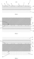
- the TBM layer may be applied by spin coating the polymer material onto the auxiliary layer 15.
- the auxiliary layer 15 may be a layer of TiN for example, but other materials are applicable when applied to a hybrid Cu/SiCN surface, for example titanium, hafnium nitride, titanium oxide, hafnium oxide or silicon oxide. These materials are removable from a Cu/SiCN hybrid surface without substantially attacking the constituent materials (Cu and SiCN) of said hybrid surface.
- the auxiliary layer 15 may be applied for example by sputter deposition, which is a form of physical vapour deposition (PVD).
- the thickness of the auxiliary layer 15 may be a few tens of nanometres, preferably between 5 nm and 100 nm.
- the wafer 1 is reversed and bonded face down to a temporary carrier wafer 17, as illustrated in Figure 4 , with the TBM layer 16 realizing a temporary adhesive bond along bonding interface 18.
- the bulk Si wafer 10 is then thinned from the back side, which may be done by grinding and/or wet etching, until the bulk Si is reduced to a thickness T as shown Figure 5 .
- the assembly of the carrier 17 and the process wafer 1 is then reversed and the back side of the thinned Si wafer 10 is bonded to an additional carrier 20 which may be an additional temporary carrier or a permanent carrier, i.e. a carrier to which the thinned wafer is bonded by a non-releasable bond or adhesive.
- an additional carrier 20 which may be an additional temporary carrier or a permanent carrier, i.e. a carrier to which the thinned wafer is bonded by a non-releasable bond or adhesive.
- the back side of the Si wafer 10 may be further thinned and subjected to processing steps, for example including the production of through-silicon vias and back side contacts.
- the temporary carrier 17 is then removed by releasing the temporary bond along interface 18, which may for example be done by heating if the TBM layer 16 is formed of a thermoplastic polymer. As shown in Figure 7 , the stack of the auxiliary layer 15 and the TBM layer 16 remains on the hybrid bonding surface 8.
- the TBM layer 16 is removed selectively with respect to the underlying auxiliary layer 15.
- This may be done by a solvent, applied by a technique known as such in the art, for example by submerging the wafer or a batch of wafers in a solvent bath for a given time.
- the solvent may be spun onto the wafer surface followed by drying the wafer surface.
- residues of the temporary bonding material may or may not remain on the surface of the auxiliary layer 15 after this TBM removal step.
- auxiliary layer 15 As illustrated in Figure 9 .
- this may be done by a wet etching step using an aqueous mixture that does not attack Cu nor SiCN. Such mixtures are known as such in the art. Even with TBM residue remaining on the TiN layer 15, this leaves the hybrid bonding surface 8 clean and essentially free of residues.
- the provision of the auxiliary layer 15 thereby enables removing the TBM layer 16 essentially without leaving any residue material.
- the hybrid bonding surface 8 is thereby ideally prepared for a hybrid bonding process to another die or wafer. This may be done in a wafer-to-wafer bonding process or in a die-to-wafer bonding process, after singulating the wafer 1 along the scribe lines 2.
- the invention is not limited to the materials and dimensions referred to with respect to the above-described exemplary embodiment.
- the method is applicable to any temporary polymer layer applied during a semiconductor production process.
- This includes for example also polymer photoresist layers applied in a lithographic process.
- Such a layer is formed of a photosensitive polymer, that is developed after illuminating the layer through a lithographic mask, so that the resist remains in a solid state according to a given pattern.
- an auxiliary layer is applied before producing the resist layer. After developing the resist, the pattern is then transferred to one or more underlying layers by etching.
- the resist is then stripped, in the manner described above for the removal of the TBM layer: by the removal of the resist selectively with respect to the auxiliary layer, followed by the selective removal of the auxiliary layer with respect to the underlying surface. Said surface is thereby left essentially clean and without residue.
- a protective layer for singulation is applied on the finished dies 3 of a wafer as shown in Figure 1a , prior to dicing the wafer, i.e. separating the dies by sawing or cutting along the scribe lines 2 by other means such as plasma etching.
- the protective layer needs to be removed after the singulation step, essentially without leaving any residues.
- an auxiliary layer is applied prior to applying the protective layer, this auxiliary layer enables removing the protective layer essentially without leaving residues, in the same manner as described above for the TBM and the photoresist layers.
- the method is applicable to different types of surfaces from which a temporary polymer layer needs to be removed without leaving residues.
- the method is for example applicable to a dielectric bonding surface as well as to a hybrid bonding surface, for example to a SiCN surface applicable in a direct SiCN-SiCN bonding process.
- a TiN layer of 10 nm thick was deposited on a wafer having a SiCN blanket layer on its surface.
- the TiN deposition was carried out by sputter deposition. Thereafter a TBM layer of 30 ⁇ m thick was spun on the TiN layer.
- the TBM was BrewerBond ® 305 available from supplier Brewer Science.
- the TBM layer was dissolved using the solvent mesitylene at 40°C during a static dissolution time of 50 min. Thereafter, residues of the TBM material remained on the TiN surface.
- the TiN layer was removed by wet etching using an aqueous mixture at 55°C during an etch time of 60s. After this, the TiN and the residues were completely removed, leaving a clean SiCN surface.
Landscapes
- Internal Circuitry In Semiconductor Integrated Circuit Devices (AREA)
- Mechanical Treatment Of Semiconductor (AREA)
Priority Applications (4)
| Application Number | Priority Date | Filing Date | Title |
|---|---|---|---|
| EP23213742.2A EP4564404A1 (de) | 2023-12-01 | 2023-12-01 | Verfahren zur entfernung von rückständen von einer substratoberfläche |
| EP24214315.4A EP4564398A1 (de) | 2023-12-01 | 2024-11-20 | Verfahren zur entfernung von rückständen von einer substratoberfläche |
| US18/960,434 US20250183088A1 (en) | 2023-12-01 | 2024-11-26 | Method for removing residues from a substrate surface |
| CN202411726644.9A CN120089600A (zh) | 2023-12-01 | 2024-11-28 | 一种从基材表面去除残留物的方法 |
Applications Claiming Priority (1)
| Application Number | Priority Date | Filing Date | Title |
|---|---|---|---|
| EP23213742.2A EP4564404A1 (de) | 2023-12-01 | 2023-12-01 | Verfahren zur entfernung von rückständen von einer substratoberfläche |
Publications (1)
| Publication Number | Publication Date |
|---|---|
| EP4564404A1 true EP4564404A1 (de) | 2025-06-04 |
Family
ID=89073191
Family Applications (2)
| Application Number | Title | Priority Date | Filing Date |
|---|---|---|---|
| EP23213742.2A Withdrawn EP4564404A1 (de) | 2023-12-01 | 2023-12-01 | Verfahren zur entfernung von rückständen von einer substratoberfläche |
| EP24214315.4A Pending EP4564398A1 (de) | 2023-12-01 | 2024-11-20 | Verfahren zur entfernung von rückständen von einer substratoberfläche |
Family Applications After (1)
| Application Number | Title | Priority Date | Filing Date |
|---|---|---|---|
| EP24214315.4A Pending EP4564398A1 (de) | 2023-12-01 | 2024-11-20 | Verfahren zur entfernung von rückständen von einer substratoberfläche |
Country Status (3)
| Country | Link |
|---|---|
| US (1) | US20250183088A1 (de) |
| EP (2) | EP4564404A1 (de) |
| CN (1) | CN120089600A (de) |
Citations (2)
| Publication number | Priority date | Publication date | Assignee | Title |
|---|---|---|---|---|
| EP3171399A1 (de) * | 2015-11-18 | 2017-05-24 | IMEC vzw | Verfahren zur vereinzelung eines stapels von halbleiterwafern |
| EP3563411B1 (de) * | 2016-12-28 | 2021-04-14 | Invensas Bonding Technologies, Inc. | Verfahren zur verarbeitung eines substrats auf einem trägersubstrat |
Family Cites Families (2)
| Publication number | Priority date | Publication date | Assignee | Title |
|---|---|---|---|---|
| EP1936678A3 (de) | 2006-12-21 | 2013-10-02 | Imec | Verfahren zum Befestigen und Ablösen eines Chips oder Substrats auf/vom einem Träger und resultierendes Zwischenerzeugnis |
| KR20090023783A (ko) * | 2007-09-03 | 2009-03-06 | 주식회사 하이닉스반도체 | 반도체 소자의 본딩패드 형성방법 |
-
2023
- 2023-12-01 EP EP23213742.2A patent/EP4564404A1/de not_active Withdrawn
-
2024
- 2024-11-20 EP EP24214315.4A patent/EP4564398A1/de active Pending
- 2024-11-26 US US18/960,434 patent/US20250183088A1/en active Pending
- 2024-11-28 CN CN202411726644.9A patent/CN120089600A/zh active Pending
Patent Citations (2)
| Publication number | Priority date | Publication date | Assignee | Title |
|---|---|---|---|---|
| EP3171399A1 (de) * | 2015-11-18 | 2017-05-24 | IMEC vzw | Verfahren zur vereinzelung eines stapels von halbleiterwafern |
| EP3563411B1 (de) * | 2016-12-28 | 2021-04-14 | Invensas Bonding Technologies, Inc. | Verfahren zur verarbeitung eines substrats auf einem trägersubstrat |
Also Published As
| Publication number | Publication date |
|---|---|
| CN120089600A (zh) | 2025-06-03 |
| US20250183088A1 (en) | 2025-06-05 |
| EP4564398A1 (de) | 2025-06-04 |
Similar Documents
| Publication | Publication Date | Title |
|---|---|---|
| US12300662B2 (en) | DBI to SI bonding for simplified handle wafer | |
| US12068278B2 (en) | Processed stacked dies | |
| US6908565B2 (en) | Etch thinning techniques for wafer-to-wafer vertical stacks | |
| CN105280473B (zh) | 减少单颗化半导体片芯中残余污染物的方法 | |
| CN110178212A (zh) | 堆栈基板的处理 | |
| US20120045611A1 (en) | Composite Carrier Structure | |
| US11476162B2 (en) | Method for dicing a semiconductor substrate into a plurality of dies | |
| CN102315198A (zh) | 具有对准标记的结构及堆叠装置的制造方法 | |
| EP2530709A1 (de) | Halbleiter-Wafer und Herstellungsverfahren dafür | |
| KR102901127B1 (ko) | 가공된 템플릿들을 이용하여 금속 상호연결 층들을 형성하는 방법들 및 시스템들 | |
| EP4564404A1 (de) | Verfahren zur entfernung von rückständen von einer substratoberfläche | |
| US7575980B2 (en) | Semiconductor device and method for manufacturing the same | |
| US20250015045A1 (en) | Method for stacking integrated circuit wafers and dies | |
| CN121310857A (zh) | 一种有环形边缘支撑结构的超薄半导体减薄方法 | |
| CN110993561A (zh) | 一种防止金属连接线断连的方法 | |
| CN121568531A (zh) | 超薄半导体实现方法以及基于超薄半导体的散热方法 | |
| KR19980028647A (ko) | 반도체장치의 제조방법 |
Legal Events
| Date | Code | Title | Description |
|---|---|---|---|
| PUAI | Public reference made under article 153(3) epc to a published international application that has entered the european phase |
Free format text: ORIGINAL CODE: 0009012 |
|
| STAA | Information on the status of an ep patent application or granted ep patent |
Free format text: STATUS: THE APPLICATION HAS BEEN PUBLISHED |
|
| AK | Designated contracting states |
Kind code of ref document: A1 Designated state(s): AL AT BE BG CH CY CZ DE DK EE ES FI FR GB GR HR HU IE IS IT LI LT LU LV MC ME MK MT NL NO PL PT RO RS SE SI SK SM TR |
|
| STAA | Information on the status of an ep patent application or granted ep patent |
Free format text: STATUS: THE APPLICATION IS DEEMED TO BE WITHDRAWN |
|
| 18D | Application deemed to be withdrawn |
Effective date: 20251205 |