EP4566986A1 - Mikroelektromechanisches bauelement mit einem metallabstandhalter - Google Patents
Mikroelektromechanisches bauelement mit einem metallabstandhalter Download PDFInfo
- Publication number
- EP4566986A1 EP4566986A1 EP23214335.4A EP23214335A EP4566986A1 EP 4566986 A1 EP4566986 A1 EP 4566986A1 EP 23214335 A EP23214335 A EP 23214335A EP 4566986 A1 EP4566986 A1 EP 4566986A1
- Authority
- EP
- European Patent Office
- Prior art keywords
- wafer
- metal
- cap wafer
- gap
- metal layer
- Prior art date
- Legal status (The legal status is an assumption and is not a legal conclusion. Google has not performed a legal analysis and makes no representation as to the accuracy of the status listed.)
- Pending
Links
Images


Classifications
-
- B—PERFORMING OPERATIONS; TRANSPORTING
- B81—MICROSTRUCTURAL TECHNOLOGY
- B81C—PROCESSES OR APPARATUS SPECIALLY ADAPTED FOR THE MANUFACTURE OR TREATMENT OF MICROSTRUCTURAL DEVICES OR SYSTEMS
- B81C1/00—Manufacture or treatment of devices or systems in or on a substrate
- B81C1/00015—Manufacture or treatment of devices or systems in or on a substrate for manufacturing microsystems
- B81C1/00261—Processes for packaging MEMS devices
- B81C1/00269—Bonding of solid lids or wafers to the substrate
-
- B—PERFORMING OPERATIONS; TRANSPORTING
- B81—MICROSTRUCTURAL TECHNOLOGY
- B81B—MICROSTRUCTURAL DEVICES OR SYSTEMS, e.g. MICROMECHANICAL DEVICES
- B81B7/00—Microstructural systems; Auxiliary parts of microstructural devices or systems
- B81B7/0032—Packages or encapsulation
- B81B7/0045—Packages or encapsulation for reducing stress inside of the package structure
- B81B7/0054—Packages or encapsulation for reducing stress inside of the package structure between other parts not provided for in B81B7/0048 - B81B7/0051
-
- B—PERFORMING OPERATIONS; TRANSPORTING
- B81—MICROSTRUCTURAL TECHNOLOGY
- B81C—PROCESSES OR APPARATUS SPECIALLY ADAPTED FOR THE MANUFACTURE OR TREATMENT OF MICROSTRUCTURAL DEVICES OR SYSTEMS
- B81C1/00—Manufacture or treatment of devices or systems in or on a substrate
- B81C1/00642—Manufacture or treatment of devices or systems in or on a substrate for improving the physical properties of a device
- B81C1/0065—Mechanical properties
- B81C1/00666—Treatments for controlling internal stress or strain in MEMS structures
-
- B—PERFORMING OPERATIONS; TRANSPORTING
- B81—MICROSTRUCTURAL TECHNOLOGY
- B81B—MICROSTRUCTURAL DEVICES OR SYSTEMS, e.g. MICROMECHANICAL DEVICES
- B81B2207/00—Microstructural systems or auxiliary parts thereof
- B81B2207/07—Interconnects
-
- B—PERFORMING OPERATIONS; TRANSPORTING
- B81—MICROSTRUCTURAL TECHNOLOGY
- B81B—MICROSTRUCTURAL DEVICES OR SYSTEMS, e.g. MICROMECHANICAL DEVICES
- B81B2207/00—Microstructural systems or auxiliary parts thereof
- B81B2207/09—Packages
- B81B2207/091—Arrangements for connecting external electrical signals to mechanical structures inside the package
- B81B2207/094—Feed-through, via
- B81B2207/095—Feed-through, via through the lid
-
- B—PERFORMING OPERATIONS; TRANSPORTING
- B81—MICROSTRUCTURAL TECHNOLOGY
- B81C—PROCESSES OR APPARATUS SPECIALLY ADAPTED FOR THE MANUFACTURE OR TREATMENT OF MICROSTRUCTURAL DEVICES OR SYSTEMS
- B81C2201/00—Manufacture or treatment of microstructural devices or systems
- B81C2201/01—Manufacture or treatment of microstructural devices or systems in or on a substrate
- B81C2201/0174—Manufacture or treatment of microstructural devices or systems in or on a substrate for making multi-layered devices, film deposition or growing
-
- B—PERFORMING OPERATIONS; TRANSPORTING
- B81—MICROSTRUCTURAL TECHNOLOGY
- B81C—PROCESSES OR APPARATUS SPECIALLY ADAPTED FOR THE MANUFACTURE OR TREATMENT OF MICROSTRUCTURAL DEVICES OR SYSTEMS
- B81C2203/00—Forming microstructural systems
- B81C2203/01—Packaging MEMS
- B81C2203/0109—Bonding an individual cap on the substrate
-
- B—PERFORMING OPERATIONS; TRANSPORTING
- B81—MICROSTRUCTURAL TECHNOLOGY
- B81C—PROCESSES OR APPARATUS SPECIALLY ADAPTED FOR THE MANUFACTURE OR TREATMENT OF MICROSTRUCTURAL DEVICES OR SYSTEMS
- B81C2203/00—Forming microstructural systems
- B81C2203/03—Bonding two components
- B81C2203/033—Thermal bonding
- B81C2203/035—Soldering
Definitions
- This disclosure relates to electronic devices and more particularly to Microelectromechanical components.
- the present disclosure further concerns eutectic bonding of microelectromechanical components with a metal standoff.
- MEMS Microelectromechanical systems
- MEMS devices also called MEMS elements, can have either simple or complex structures with various moving parts. They include devices such as gyroscopes, acceleration sensors, magnetometers, and pressure sensors. MEMS devices may be fabricated from a silicon wafer by microfabrication techniques.
- Electronic chips also called dies, are prepared by manufacturing various electronic structures on a substrate and cutting the substrate into small, chip-size pieces. These chips may be MEMS devices. Several MEMS elements may be built on the same die. This allows significant cost and area reduction. Once the MEMS elements are built, they may need to be sealed in a particular environment depending on their function.
- Eutectic bonding also known as eutectic soldering, is a well-established semiconductor bonding technology that involves bonding wafers together by high pressure using a seal formed of two or more metal films which transform into a eutectic alloy at a specific temperature (eutectic temperature). Due to their easy preparation techniques and good wettability, eutectic alloys form excellent seals in electronic devices. Eutectic bonding is widely used in MEMS technology for the hermetic sealing of MEMS components. During the bonding process, at the eutectic temperature, the eutectic alloy is in liquid phase.
- An object of the present disclosure is to provide a solution to the problem described above.
- the disclosed solution allows MEMS vertical gap height control in eutectically bonded microelectromechanical components. Examples provided in this disclosure describe ways to implement the solution. The improvement is achieved by features of the microelectromechanical component and a manufacturing method.
- the disclosure describes a microelectromechanical component comprising a cap wafer and a structure wafer.
- the cap wafer has a top surface and a bottom surface, and the top surface of the cap wafer defines a horizontal xy-plane and a vertical z-direction which is perpendicular to the xy-plane.
- the structure wafer has a top surface and a bottom surface. The cap wafer and the structure wafer are bonded to each other so that the cap wafer and the structure wafer are aligned with each other in the z-direction.
- the microelectromechanical component further comprises an electrical connection and a gap-control region, and the electrical connection is in the gap-control region.
- the electrical connection comprises a metal layer.
- any direction or plane which is parallel to the xy-plane defined by the cap wafer can be called horizontal.
- the direction which is perpendicular to the xy-plane can be called vertical direction.
- Expressions such as “top”, “bottom”, “above”, “below”, “up” and “down” refer in this disclosure to differences in the vertical z-coordinate. These expressions do not imply anything about how the device should be oriented with respect to the earth's gravitational field when the component is in use or when it is being manufactured.
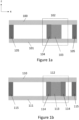
- Figure 1a illustrates an example of the sectional view of a microelectromechanical component comprising a metal standoff 104.
- the cap wafer 100 and the structure wafer 101 are bonded to each other via a seal 105 so that the cap wafer and the structure wafer are aligned with each other in the z-direction.
- the seal 105 may be a eutectic seal which is formed by two or more metals or by a combination of one or more metals and a metalloid which transform into a eutectic alloy at a specific temperature.
- the microelectromechanical component further comprises a gap-control region 102 and an electrical connection located in the gap-control region 102. The electrical connection may connect the cap wafer to the structure wafer.
- This connection may for example connect electrical signals and/or electrical potentials between the micromechanical structure and system electronics.
- the electrical connection comprises a metal layer 103.
- the metal layer 103 is attached to the bottom surface of the cap wafer 100 and extends in the z-direction from the bottom surface of the cap wafer 100 to the top surface of the structure wafer 101.
- the microelectromechanical component further comprises a metal standoff 104.
- the metal standoff 104 is attached to the bottom surface of the cap wafer 100 in the gap-control region 102.
- the metal standoff 104 is adjacent to the metal layer 103 and extends in the z-direction from the bottom surface of the cap wafer 100 to the top surface the structure wafer 101.
- the metal standoff 104 is in contact with the metal layer 103.
- the metal standoff may be beside the metal layer. This option may apply to any embodiment in this disclosure.
- the surface area of the metal standoff in the xy-plane may be of the same order of magnitude or larger than the surface of metal layer 103 in the xy-plane.
- the one or more metal standoffs may comprise Ti, or the one or more metal standoffs may comprise W.
- the metal standoff 104 may be made of one or more metals that include but are not limited to Ti, W, Cr, V, or hard metal alloys, or hard metalloid.
- the metal layer 103 in the electrical connection may be made of one or more metals that include but are not limited to Al, Au, Ag, Cu, Sn, or soft metal alloys. These options may apply to any embodiment in this disclosure.
- the compressive strength of the one or more metals forming the metal standoff 104 is greater than the compressive strength of the one or more metals forming the metal layer 103.
- the one or more metals composing the metal layer 103 are softer than the one or more metals composing the metal standoff 104.
- the metal standoff may be formed by a variety of deposition methods such as sputtering, chemical vapor deposition, molecular beam epitaxy, electron beam physical vapor evaporation, atomic layer deposition, or laser metal deposition.
- the metal layer may be formed by a variety of deposition methods such as sputtering, chemical vapor deposition, molecular beam epitaxy, electron beam physical vapor evaporation, atomic layer deposition, or laser metal deposition. These options may apply to any embodiment in this disclosure.
- the metal layer may serve as an ohmic contact in the MEMS, due to its hardness, the metal standoff provides an accurate control of the MEMS gap height during the eutectic bonding of the component, mechanical stress reduction of the electrical contact, as well as the possibility for element size reduction.
- the microelectromechanical component may comprise a plurality of metal standoffs.
- the metal standoffs may be substantially evenly distributed around the metal layer.
- Figure 1b illustrates an example of the sectional view of a microelectromechanical component comprising a plurality of metal standoffs.
- the electrical connection comprises a metal layer 113.
- the metal layer 113 is attached to the bottom surface of the cap wafer 110 in the gap-control region 112 and extends in the z-direction from the bottom surface of the cap wafer 110 to the top surface of the structure wafer 111.
- the microelectromechanical component further comprises two metal standoffs 114 in the gap-control region 112.
- the metal standoffs 114 which are both adjacent to the metal layer 113, are opposite to each other on different sides of the metal layer 113.
- the metal standoffs 114 are attached to the bottom surface of the cap wafer 110 and extend in the z-direction from the bottom surface of the cap wafer 110 to the top surface the structure wafer 111.
- Reference number 115 in figure 1b corresponds to reference numbers 105 in figure 1a .
- the cap wafer may be a semiconducting wafer, or an insulating wafer such as a glass layer, or a wafer comprising semiconducting parts and insulating parts, or a wafer comprising metal parts and insulating parts, or integrated circuitry (IC).
- the insulating parts may be made of glass or other insulating materials such as silicon dioxide, silicon nitride or aluminium oxide. These options may apply to any embodiment in this disclosure.
- the structure wafer may be a semiconductor device layer which has been attached to a support layer (not illustrated).
- the device layer may be a layer of silicon.
- the device layer and the support layer may for example be parts of a silicon-on-insulator (SOI) substrate where MEMS elements can be formed by patterning the top silicon layer (the device layer).
- SOI silicon-on-insulator
- the electrical connection may further comprise an electrically conductive via.
- the electrically conductive via may extend along the z-direction through the cap wafer, and the metal layer may extend along the bottom surface of the cap wafer so that it meets the electrically conductive via.
- the electrically conductive via may extend through a portion of the cap wafer thickness. Alternatively, the electrically conductive via may extend through the whole cap wafer thickness.
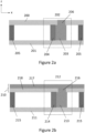
- Figure 2a illustrates another example of the sectional view of the microelectromechanical component comprising a metal standoff.
- the cap wafer 200 and the structure wafer 201 are bonded to each other via a seal 205 so that the cap wafer and the structure wafer are aligned with each other in the z-direction.
- the microelectromechanical component further comprises a gap-control region 202 and an electrical connection in the gap-control region.
- the electrical connection comprises a metal layer 203 and an electrically conductive via 206.
- the electrically conductive via 206 extends along the z-direction through the cap wafer thickness.
- the metal layer 203 extends in the x-direction along the bottom surface of the cap wafer so that it meets the electrically conductive via 206 and extends along the z-direction from the bottom surface of the cap wafer 200 to the top surface of the structure wafer 201.
- the metal layer 203 may be connected to an external electrical connection through the electrically conductive via 206.
- the cap wafer may be an insulating wafer such as a glass wafer.
- the electrically conductive via may comprise a semiconducting material such as Si.
- the electrically conductive via may comprise a metal such as Al, Au, Ag, Cu, Sn, or a metal alloy.
- the electrically conductive via and the metal layer may be made of the same metal.
- the microelectromechanical component further comprises a metal standoff 204 in the gap-control region, wherein the metal standoff 204 is adjacent to the metal layer 203.
- the metal standoff 204 is attached to the bottom surface of the cap wafer and extends in the z-direction from the bottom surface of the cap wafer 200 to the top surface the structure wafer 201.
- the cap wafer may comprise a semiconducting part and an insulating part, wherein the semiconducting part is located on top of the insulating part so that the bottom surface of the insulating part forms the bottom surface of the cap wafer.
- the cap wafer may comprise a conductive part, such as a metal part, and an insulating part, wherein the metal part is located on top of the insulating part so that the bottom surface of the insulating part forms the bottom surface of the cap wafer.
- Figure 2b illustrates an example of the sectional view of a microelectromechanical component comprising a metal standoff.
- the microelectromechanical component comprises a cap wafer 210 and a structure wafer 211 which are bonded together via a seal 215.
- the cap wafer comprises a semiconducting part 217 and an insulating part 218.
- the semiconducting part 217 is located on top of the insulating part 218.
- the microelectromechanical component further comprises an electrical connection in the gap-control region 212.
- the electrical connection comprises an electrically conductive via 216, and the electrically conductive via 216 extends along the z-axis from the bottom side of the semiconducting part 217 to the bottom side of the insulating part 218 so that the insulating part surrounds the sides of the electrically conductive via 216.
- Reference numbers 213 and 214 in figure 2b correspond to reference numbers 203 and 204, respectively, in figure 2a .
- the top surface of the structure wafer may comprise a protrusion wherein the protrusion is located in the gap-control region.
- the metal layer may extend from the bottom surface of the cap wafer to the protrusion, and the one or more metal standoffs may extend in the z-direction from the bottom surface of the cap wafer to the protrusion.
- the metal layer and the protrusion, which acts as an anchor, may serve as a good ohmic press-on contact inside the element.
- the protrusion may have different shapes such as a truncated pyramid shape, or a pillar-like shape.
- the pillar like-shape may be, but is not limited to, a cylinder, a hexagonal prism, or a cuboid. These options may apply to any embodiment in this disclosure.
- Figure 3a illustrates another example of the sectional view of a microelectromechanical component comprising a metal standoff.
- the cap wafer 300 and the structure wafer 301 are bonded together via a seal 305.
- the microelectromechanical component comprises an electrical connection, and the electrical connection comprises an electrically conductive via 306 and a metal layer 303.
- the electrically conductive via 306 extends along the z-axis through the cap wafer thickness
- the metal layer 303 extends in the x-direction along the bottom surface of the cap wafer so that it meets the bottom side of the electrically conductive via 306.
- the microelectromechanical component further comprises a metal standoff 304 which is adjacent to the metal layer 303.
- the metal layer 303 overlaps the metal standoff 304.
- the metal layer 303 extends in the x-direction so that it covers a portion of the metal standoff 304.
- the compressive strength of the one or more metals forming the metal standoff 304 is greater than the compressive strength of the one or more metals forming the metal layer 303.
- the top surface of the structure wafer 301 comprises a protrusion 309 in the gap-control region 302.
- the protrusion 309 bulges out in the z-direction so that it meets the metal standoff 304 and the metal layer 303.
- the protrusion may be formed by semiconductor microfabrication techniques such as LOCOS process, wet etching process or dry etching process. These options may apply to any embodiment in this disclosure.
- Figure 3b illustrates another example of the sectional view of a microelectromechanical component with metal standoffs.
- the electrical connection comprises an electrically conductive via 316 and a metal layer 313.
- the electrically conductive via 316 extends along the z-axis through the cap wafer thickness, and the metal layer 313 extends along the bottom surface of the cap wafer 310 so that it meets the bottom side of the electrically conductive via 316.
- the top surface of the structure wafer 311 comprises a protrusion 319 in the gap-control region 312.
- the protrusion 319 has a multi-height step-pyramid-like shape.
- the step-pyramid comprises a summit and side steps.
- the distance in the z-direction from the bottom surface of the cap wafer to the summit is less than the distance in the z-direction from bottom surface of the cap wafer to the side steps.
- the protrusion 319 extends in the z-direction so that its summit meets the metal layer 313.
- the microelectromechanical component further comprises two metal standoffs 314 which are adjacent to the metal layer 313 and are located opposite to each other on different sides of the metal layer 313.
- the metal standoffs 314 extend along the z-direction from the bottom surface of the cap wafer to the protrusion so that the bottom of each metal standoff is in contact with a side step.
- the compressive strength of the one or more metals forming the metal standoffs 314 is greater than the compressive strength of the one or more metals forming the metal layer 313 in the electrical connection.
- Reference number 315 in figure 3b corresponds to reference number 305 in figure 3a .
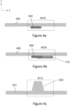
- FIGS 4a-4e provide a simplified illustration of an example method for manufacturing a microelectromechanical component with a metal standoff.
- the microelectromechanical element comprises a cap wafer and a structure wafer.
- the cap wafer has a top surface and a bottom surface, and the top surface of the cap wafer defines a horizontal xy-plane and a vertical z-direction which is perpendicular to the xy-plane.
- the cap wafer comprises a cap wafer gap-control region.
- the structure wafer has a top surface and a bottom surface.
- the structure wafer comprises a structure wafer gap-control region.
- the method comprises: (1) forming one or more metal standoffs at the bottom surface of the cap wafer in the cap wafer gap-control region, (2) forming a metal layer on the bottom surface of the cap wafer in the cap wafer gap-control region so that the metal layer is adjacent to the one or more metal standoffs, (3) placing the cap wafer on top of the structure wafer so that the cap wafer gap-control region is aligned with the structure wafer gap-control region in the z-direction, (4) bonding the cap wafer and the structure wafer together so that the metal layer extends in the z-direction from the bottom surface of the cap wafer to the top surface of the structure wafer and the one or more metal standoffs extend in the z-direction from the bottom surface of the cap wafer to the top surface of the structure wafer.
- the compressive strength of the metal forming the one or more metal standoffs is greater than the compressive strength of the metal layer in the electrical connection.
- the structure wafer may be a semiconductor device layer which has been attached to a support layer.
- the device layer may be a layer of silicon.
- the device layer and the support layer may for example be parts of a silicon-on-insulator (SOI) substrate where MEMS elements can be formed by patterning the top silicon layer (the device layer).
- SOI silicon-on-insulator
- the cap wafer may be a semiconducting wafer, or an insulating wafer such as a glass layer, or a wafer comprising semiconducting parts and insulating parts, or a wafer comprising metal parts and insulating parts or integrated circuitry (IC).
- the insulating parts may be made of glass or other insulating materials such as silicon dioxide, silicon nitride or aluminium oxide.
- Figure 4a illustrates one of the first steps in the example method for manufacturing a microelectromechanical component with a metal standoff. This step comprises forming a metal standoff 404 at the bottom surface of the cap wafer 400 in the cap wafer gap-control region 4010.
- Figure 4b illustrates another step in the example method for manufacturing a microelectromechanical component with a metal standoff.
- This step comprises forming a metal layer 413 on the bottom surface of the cap wafer 400 in the cap wafer gap-control region 4010, so that the metal layer 413 is adjacent to the metal standoff 404.
- the metal layer 413 overlaps the metal standoff 404.
- the metal layer 413 extends in the x-direction so that it covers partly the bottom surface of the metal standoff 404.
- the compressive strength of the one or more metals forming the metal standoff 404 is greater than the compressive strength of the one or more metals forming the metal layer 413.
- the metal layer is more malleable than the metal standoff.
- the metal standoff provides an accurate control of the MEMS gap height during the eutectic bonging of the component.
- the method may comprise forming a protrusion in the structure wafer gap-control region before placing the cap wafer on top of the structure wafer so that the top surface of the structure wafer comprises the protrusion.
- Figure 4c illustrates the step of forming a protrusion 429 in the structure wafer gap-control region 4211 so that the top surface of the structure wafer 421 comprises the protrusion 429.
- the protrusion 429 bulges upward and is aligned with the metal standoff 404 and the metal layer 413 in the z-direction.
- the protrusion 429 may be formed by semiconductor microfabrication techniques such as LOCOS process, wet etching process or dry etching process. These options may apply to any embodiment in this disclosure.
- Figure 4d illustrates a further step in the example method for manufacturing a microelectromechanical component with a metal standoff.
- This step comprises placing the cap wafer 400 on top of the structure wafer 421 so that the cap wafer gap-control region 4010 is aligned with the structure wafer gap-control region 4211 in the z-direction.
- the protrusion 429 is aligned with the metal standoff 404 and the metal layer 413 in the z-direction.
- Figure 4e illustrates the final step in the example method for manufacturing a microelectromechanical component with a metal standoff.
- This step comprises bonding the cap wafer 400 and the structure wafer 421 together so that the metal layer 413 extends in the z-direction from the bottom surface of the cap wafer 400 to the top surface of the structure wafer 421 and the one or more metal standoffs 404 extend in the z-direction from the bottom surface of the cap wafer 400 to the top surface of the structure wafer 421.
- the metal layer 413 and the metal standoff 404 extend in the z-direction from the bottom surface of the cap wafer 400 to the protrusion 429.
- the cap wafer 400 and the structure wafer 421 may be eutectically bonded together via a eutectic seal 435.
- the method for manufacturing a microelectromechanical component may comprise the step of forming an electrically conductive via in the cap wafer gap-control region before forming the one or more metal standoffs at the bottom surface of the cap wafer.
- the electrically conductive via may extend along the z-direction through the cap wafer and the metal layer may meet the bottom of the electrically conductive via.
- the electrically conductive via may extend through a portion of the cap wafer thickness. Alternatively, the electrically conductive via may extend through the whole cap wafer thickness.
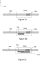
- Figures 5a-5d illustrate a few steps in the example method for manufacturing a microelectromechanical component wherein the cap wafer comprises an electrically conductive via.
- Figure 5 a illustrates the step of forming an electrically conductive via 506 in the cap wafer gap-control region 5010 before forming the one or more standoffs.
- the electrically conductive via extends along the z-direction through the cap wafer 500.
- the cap wafer may be an insulating wafer such as a glass layer.
- the electrically conductive via 506 may comprise a semiconducting material.
- the electrically conductive via may comprise a metal.
- Figure 5b illustrates a further step in the example method for manufacturing a microelectromechanical component with a metal standoff. This step comprises forming a metal standoff 514 at the bottom surface of the cap wafer 500 in the cap wafer gap-control region 5010.
- Figure 5c illustrates another step in the example method for manufacturing a microelectromechanical component with a metal standoff.
- This step comprises forming a metal layer 523 on the bottom surface of the cap wafer 500 in the cap wafer gap-control region 5010, so that the metal layer 523 is adjacent to the metal standoff 514 and that the metal layer 523 meets the electrically conductive via 506.
- the metal layer 523 extends in the x-direction so that it covers partly the bottom surface of the metal standoff 514.
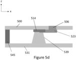
- Figure 5d illustrates the final step in the example method for manufacturing a microelectromechanical component with a metal standoff.
- This step comprises bonding the cap wafer 500 and the structure wafer 531 together so that the metal layer 523 extends in the z-direction from the bottom surface of the cap wafer 500 to the top surface of the structure wafer 531 and the metal standoff 514 extends in the z-direction from the bottom surface of the cap wafer 500 to the top surface of the structure wafer 531.
- the metal layer 523 and the metal standoff 514 extend from the bottom surface of the cap wafer 500 to the protrusion 539.
- Reference number 545 in figure 5c corresponds to reference number 435 in figure 4e .
Landscapes
- Engineering & Computer Science (AREA)
- Microelectronics & Electronic Packaging (AREA)
- Manufacturing & Machinery (AREA)
- Mechanical Engineering (AREA)
- Computer Hardware Design (AREA)
- Micromachines (AREA)
Priority Applications (2)
| Application Number | Priority Date | Filing Date | Title |
|---|---|---|---|
| EP23214335.4A EP4566986A1 (de) | 2023-12-05 | 2023-12-05 | Mikroelektromechanisches bauelement mit einem metallabstandhalter |
| US18/965,325 US20250178887A1 (en) | 2023-12-05 | 2024-12-02 | Microelectromechanical component with a metal standoff |
Applications Claiming Priority (1)
| Application Number | Priority Date | Filing Date | Title |
|---|---|---|---|
| EP23214335.4A EP4566986A1 (de) | 2023-12-05 | 2023-12-05 | Mikroelektromechanisches bauelement mit einem metallabstandhalter |
Publications (1)
| Publication Number | Publication Date |
|---|---|
| EP4566986A1 true EP4566986A1 (de) | 2025-06-11 |
Family
ID=89119453
Family Applications (1)
| Application Number | Title | Priority Date | Filing Date |
|---|---|---|---|
| EP23214335.4A Pending EP4566986A1 (de) | 2023-12-05 | 2023-12-05 | Mikroelektromechanisches bauelement mit einem metallabstandhalter |
Country Status (2)
| Country | Link |
|---|---|
| US (1) | US20250178887A1 (de) |
| EP (1) | EP4566986A1 (de) |
Citations (2)
| Publication number | Priority date | Publication date | Assignee | Title |
|---|---|---|---|---|
| US20060208326A1 (en) * | 2005-03-18 | 2006-09-21 | Nasiri Steven S | Method of fabrication of ai/ge bonding in a wafer packaging environment and a product produced therefrom |
| US10308507B2 (en) | 2015-10-28 | 2019-06-04 | Invensense, Inc. | MEMS gap control structures |
-
2023
- 2023-12-05 EP EP23214335.4A patent/EP4566986A1/de active Pending
-
2024
- 2024-12-02 US US18/965,325 patent/US20250178887A1/en active Pending
Patent Citations (2)
| Publication number | Priority date | Publication date | Assignee | Title |
|---|---|---|---|---|
| US20060208326A1 (en) * | 2005-03-18 | 2006-09-21 | Nasiri Steven S | Method of fabrication of ai/ge bonding in a wafer packaging environment and a product produced therefrom |
| US10308507B2 (en) | 2015-10-28 | 2019-06-04 | Invensense, Inc. | MEMS gap control structures |
Also Published As
| Publication number | Publication date |
|---|---|
| US20250178887A1 (en) | 2025-06-05 |
Similar Documents
| Publication | Publication Date | Title |
|---|---|---|
| US7259436B2 (en) | Micromechanical component and corresponding production method | |
| EP0742581B1 (de) | Versiegelte Hohlraumanordnung | |
| US10040681B2 (en) | Method and system for MEMS devices | |
| EP3044162B1 (de) | Verfahren zur hermetischen verpackung auf waferebene mit vertikalen durchführungen | |
| US8049326B2 (en) | Environment-resistant module, micropackage and methods of manufacturing same | |
| CN106145024B (zh) | 运动微机电系统(mems)封装件 | |
| US7964428B2 (en) | Micromechanical component and method for fabricating a micromechanical component | |
| EP3135632B1 (de) | Cmos-mems integration mit metallsilizidbildung | |
| US9834435B1 (en) | Structure and formation method of semiconductor device structure | |
| US20060211177A1 (en) | Structure and process for packaging RF MEMS and other devices | |
| CN104973564A (zh) | 用于共晶键合两个载体装置的方法 | |
| WO2016200346A1 (en) | Hermetic packaging method for soi-mems devices with embedded vertical feedthroughs | |
| EP4566986A1 (de) | Mikroelektromechanisches bauelement mit einem metallabstandhalter | |
| US8378433B2 (en) | Semiconductor device with a controlled cavity and method of formation | |
| EP4375232B1 (de) | Verfahren zum bonden einer mikroelektromechanischen vorrichtung | |
| EP4530249B1 (de) | Mikroelektromechanisches bauelement mit spaltsteuerungsstruktur und verfahren zu seiner herstellung | |
| TWI915944B (zh) | 微機電構件及其製造方法 | |
| FI131218B1 (en) | Device and method for centering bonding force | |
| US20250230037A1 (en) | Micro-electro-mechanical system package and fabrication method thereof | |
| CN119568984A (zh) | 微机电封装及其制造方法 |
Legal Events
| Date | Code | Title | Description |
|---|---|---|---|
| PUAI | Public reference made under article 153(3) epc to a published international application that has entered the european phase |
Free format text: ORIGINAL CODE: 0009012 |
|
| STAA | Information on the status of an ep patent application or granted ep patent |
Free format text: STATUS: REQUEST FOR EXAMINATION WAS MADE |
|
| 17P | Request for examination filed |
Effective date: 20231205 |
|
| AK | Designated contracting states |
Kind code of ref document: A1 Designated state(s): AL AT BE BG CH CY CZ DE DK EE ES FI FR GB GR HR HU IE IS IT LI LT LU LV MC ME MK MT NL NO PL PT RO RS SE SI SK SM TR |