EP4567480A1 - Optischer splitter, optischer splitterchip, kommunikationsvorrichtung und optisches verteilungsnetzwerk - Google Patents
Optischer splitter, optischer splitterchip, kommunikationsvorrichtung und optisches verteilungsnetzwerk Download PDFInfo
- Publication number
- EP4567480A1 EP4567480A1 EP23859360.2A EP23859360A EP4567480A1 EP 4567480 A1 EP4567480 A1 EP 4567480A1 EP 23859360 A EP23859360 A EP 23859360A EP 4567480 A1 EP4567480 A1 EP 4567480A1
- Authority
- EP
- European Patent Office
- Prior art keywords
- optical
- waveguide
- splitting
- optical splitting
- segment
- Prior art date
- Legal status (The legal status is an assumption and is not a legal conclusion. Google has not performed a legal analysis and makes no representation as to the accuracy of the status listed.)
- Pending
Links
Images




Classifications
-
- G—PHYSICS
- G02—OPTICS
- G02B—OPTICAL ELEMENTS, SYSTEMS OR APPARATUS
- G02B6/00—Light guides; Structural details of arrangements comprising light guides and other optical elements, e.g. couplings
- G02B6/10—Light guides; Structural details of arrangements comprising light guides and other optical elements, e.g. couplings of the optical waveguide type
- G02B6/12—Light guides; Structural details of arrangements comprising light guides and other optical elements, e.g. couplings of the optical waveguide type of the integrated circuit kind
-
- G—PHYSICS
- G02—OPTICS
- G02B—OPTICAL ELEMENTS, SYSTEMS OR APPARATUS
- G02B6/00—Light guides; Structural details of arrangements comprising light guides and other optical elements, e.g. couplings
- G02B6/24—Coupling light guides
- G02B6/26—Optical coupling means
- G02B6/28—Optical coupling means having data bus means, i.e. plural waveguides interconnected and providing an inherently bidirectional system by mixing and splitting signals
- G02B6/2804—Optical coupling means having data bus means, i.e. plural waveguides interconnected and providing an inherently bidirectional system by mixing and splitting signals forming multipart couplers without wavelength selective elements, e.g. "T" couplers, star couplers
- G02B6/2821—Optical coupling means having data bus means, i.e. plural waveguides interconnected and providing an inherently bidirectional system by mixing and splitting signals forming multipart couplers without wavelength selective elements, e.g. "T" couplers, star couplers using lateral coupling between contiguous fibres to split or combine optical signals
-
- G—PHYSICS
- G02—OPTICS
- G02B—OPTICAL ELEMENTS, SYSTEMS OR APPARATUS
- G02B6/00—Light guides; Structural details of arrangements comprising light guides and other optical elements, e.g. couplings
- G02B6/10—Light guides; Structural details of arrangements comprising light guides and other optical elements, e.g. couplings of the optical waveguide type
- G02B6/12—Light guides; Structural details of arrangements comprising light guides and other optical elements, e.g. couplings of the optical waveguide type of the integrated circuit kind
- G02B6/122—Basic optical elements, e.g. light-guiding paths
- G02B6/125—Bends, branchings or intersections
-
- G—PHYSICS
- G02—OPTICS
- G02B—OPTICAL ELEMENTS, SYSTEMS OR APPARATUS
- G02B6/00—Light guides; Structural details of arrangements comprising light guides and other optical elements, e.g. couplings
- G02B6/10—Light guides; Structural details of arrangements comprising light guides and other optical elements, e.g. couplings of the optical waveguide type
- G02B6/12—Light guides; Structural details of arrangements comprising light guides and other optical elements, e.g. couplings of the optical waveguide type of the integrated circuit kind
- G02B2006/12083—Constructional arrangements
- G02B2006/12111—Fibre
-
- G—PHYSICS
- G02—OPTICS
- G02B—OPTICAL ELEMENTS, SYSTEMS OR APPARATUS
- G02B6/00—Light guides; Structural details of arrangements comprising light guides and other optical elements, e.g. couplings
- G02B6/10—Light guides; Structural details of arrangements comprising light guides and other optical elements, e.g. couplings of the optical waveguide type
- G02B6/12—Light guides; Structural details of arrangements comprising light guides and other optical elements, e.g. couplings of the optical waveguide type of the integrated circuit kind
- G02B2006/12133—Functions
- G02B2006/1215—Splitter
Definitions
- This application relates to the field of optical energy loss technologies of an optical splitter, and in particular, to an optical splitter, an optical splitter chip, a communication device, and an optical distribution network.
- a splitter is a key component of a optical distribution network (ODN) communication network.
- ODN optical distribution network
- a link loss is large, resulting in a short access distance and low network redundancy.
- a main reason is that a loss of the optical splitter is large.
- the loss of the optical splitter mainly includes a waveguide loss (design and process), a coupling loss between a fiber array (FA) and a waveguide, and a connector loss.
- Key factors for forming the waveguide loss include an optical splitting loss of branching, a waveguide bending loss, and a transmission loss.
- a main reason of a branching loss is as follows: Light is transmitted in a straight waveguide in a form of fundamental mode. At a position of branching, a mode field of the fundamental mode is distorted (one branch is divided into a plurality of branches), causing a mode field mismatch and the branching loss.
- a main reason of the bending loss is as follows: Light is transmitted in a bent waveguide. Because the waveguide is bent, optical mode field distribution is not transmission at a center of a straight waveguide as optical mode field distribution is when light is transmitted in the straight waveguide, but is off-center energy transmission. As a result, an optical splitting ratio changes when subsequent branching continues, and energy distribution consistency of subsequent branching is poor.
- Optical splitters are classified into even optical splitting and uneven optical splitting.
- FTTH fiber to the home
- This application provides an optical splitter, an optical splitter chip, a communication device, and an optical distribution network. Positions of branch waveguides are distributed, and a first optical splitting waveguide is disposed between second optical splitting waveguides, so that energy optical splitting can be disposed in a low-energy region of an optical signal. This reduces a loss generated during optical splitting of the optical signal.
- this application provides an optical splitter.
- the optical splitter includes an optical input waveguide and an optical splitting waveguide, where the optical input waveguide is configured to receive an optical signal;
- the optical splitting waveguide includes a first optical splitting waveguide and a plurality of second optical splitting waveguides; the first optical splitting waveguide and the second optical splitting waveguide are coplanar, and the plurality of second optical splitting waveguides are divided into two parts and located on two sides of the first optical splitting waveguide, or the plurality of second optical splitting waveguides are sequentially spaced apart along a circumferential direction of the first optical splitting waveguide;
- the first optical splitting waveguide includes a first connection segment connected to the optical input waveguide, and the first connection segment is in a straight-line shape.
- the first optical splitting waveguide is disposed between the second optical splitting waveguides, so that an optical splitting line can be effectively disposed in a low-energy region of the optical signal.
- the first optical splitting waveguide is located between the plurality of second optical splitting waveguides, and at least a part of the first optical splitting waveguide is in a straight-line shape, so that an optical signal can be efficiently transmitted, to reduce an energy loss.
- a cross-sectional area of the first optical splitting waveguide is greater than a cross-sectional area of the second optical splitting waveguide, so that the first optical splitting waveguide has a large energy proportion.
- the first optical splitting waveguide is located between the plurality of second optical splitting waveguides, and the optical splitting line of the first optical splitting waveguide and the second optical splitting waveguide is located in the low-energy region. This reduces an energy branching loss.
- the second optical splitting waveguide includes a second connection segment and a second transmission segment, the second connection segment is located between the first transition waveguide and the second transmission segment, and an optical signal sequentially flows through the second connection segment and the second transmission segment; and both the second connection segment and the second transmission segment are arc-shaped, the second connection segment bends along a transmission direction of the optical signal toward a direction away from the first optical splitting waveguide, and the second transmission segment bends along the transmission direction of the optical signal toward a direction close to the first optical splitting waveguide.
- the second optical splitting waveguide is of a double-arc-shaped structure, so that there is a specific gap between a light output end of the second optical splitting waveguide and a light output end of the first optical splitting waveguide, to facilitate connection to a back-end fiber and also facilitate cascading with an optical branching element to continue optical splitting.
- the second connection segment and the second transmission segment are tangent at a bordering position, to ensure that the optical signal is transmitted in a smooth transition waveguide when being transmitted in the second optical splitting waveguide. This prevents an optical energy loss.
- the second optical splitting segment further includes a third transmission segment, the third transmission segment is located between the second connection segment and the second transmission segment, the third transmission segment is in a straight-line shape, the third transmission segment and the second connection segment are tangent at a bordering position, and the third transmission segment and the second transmission segment are tangent at a bordering position.
- the third transmission segment is disposed as a straight-line segment, to increase a gap between the second branch waveguide and the first branch waveguide without increasing a length of a bent part in the second optical splitting waveguide, so that a large energy loss caused by a long path that is of a bent waveguide and through which an optical signal passes is avoided.
- a cross-sectional area of at least a section of the second connection segment smoothly increases along the transmission direction of the optical signal, and a cross-sectional area of at least a section of the second transmission segment smoothly decreases along the transmission direction of the optical signal, to form a second optical splitting waveguide of a thin-thick-thin structure.
- the second optical splitting waveguide further includes an optical branching element
- the second transmission segment is cascaded with at least one optical branching element at the light output end
- all the second optical splitting waveguides in the optical splitter have N2 waveguide output ports in total, and N2 is an even number greater than or equal to 4.
- the light output end of the second transmission segment is cascaded with the optical branching element, so that all the second optical splitting waveguides have N2 light output ports, and energy of each light output port is the same.
- the optical branching element includes a second transition waveguide and a plurality of optical branching waveguides, the optical signal enters the second transition waveguide and is split into a plurality of optical signals, and the plurality of optical signals enter the optical branching waveguides in a one-to-one manner.
- the optical signal enters the second transition waveguide from the second transmission segment, is split in the second transition waveguide and then enters the plurality of optical branching waveguides respectively.
- the optical signal is split into a plurality of balanced optical signals.
- the optical branching waveguide includes a first optical splitting branch waveguide, a quantity of first optical splitting branch waveguides is two, the first optical splitting branch waveguide includes a first arc-shaped segment and a second arc-shaped segment, the first arc-shaped segment bends along a transmission direction of the optical signal toward a direction away from the other first optical splitting branch waveguide, and the second arc-shaped segment bends along the transmission direction of the optical signal toward a direction close to the other first optical splitting branch waveguide.
- the first optical splitting branch waveguide is of a double-arc-shaped structure, so that when the second transmission segment outputs the optical signal, the optical signal can be split and then enter the plurality of first optical splitting branch waveguides, and specific gaps exist between light output ports of the plurality of first optical splitting branch waveguides, to facilitate connection to a back-end fiber.
- a cross-sectional area of at least a section of the first arc-shaped segment smoothly increases along the transmission direction of the optical signal
- a cross-sectional area of at least a section of the second arc-shaped segment smoothly decreases along the transmission direction of the optical signal.
- the first optical splitting branch waveguide is disposed in a thin-thick-thin structure. This effectively reduces a center deviation that occurs when an optical signal is transmitted in a bent waveguide, and improves balance of back-end optical splitting.
- the optical branching waveguide further includes a second optical splitting branch waveguide, the second optical splitting branch waveguide is located between the two first optical splitting branch waveguides, and a section that is of the second optical splitting branch waveguide and that is connected to the second transition waveguide is in a straight-line shape.
- the second optical splitting branch waveguide is disposed, and the second optical splitting branch waveguide is disposed between the first optical splitting branch waveguides, to effectively reduce an optical splitting loss of an optical signal in the optical branching element.
- the optical splitter further includes a first transition waveguide, the first transition waveguide is located between the optical input waveguide and the optical splitting waveguide, the optical signal is transmitted from the optical input waveguide into the first transition waveguide, and is split into a first optical signal and a plurality of second optical signals in the first transition waveguide, the first optical signal enters the first optical splitting waveguide, the plurality of second optical signals enter the second optical splitting waveguides in a one-to-one manner, and an energy value of the first optical signal is greater than an energy value of each second optical signal.
- the first transition waveguide is used to connect the optical input waveguide and the branch waveguide.
- the optical signal is split into the first optical signal and the second optical signal in the first transition waveguide.
- the first optical signal has a larger energy proportion and enters the first optical splitting waveguide
- the second optical signal has a smaller energy proportion and enters the second optical splitting waveguide.
- the optical splitter further includes a substrate, the first optical splitting waveguide and the second optical splitting waveguide are both located in the substrate, and the first optical splitting waveguide and the second optical splitting waveguide are coplanar.
- the first optical splitting waveguide and the second optical splitting waveguide are formed in the substrate, and the first optical splitting waveguide is located between the second optical splitting waveguides, to form an uneven optical splitter in a form of planar waveguide, so that a branching loss of the optical splitter is low.
- a quantity of second optical splitting waveguides is an even number
- the plurality of second optical splitting waveguides are evenly divided into two parts
- the two parts of the second optical splitting waveguides are mirror-symmetric to each other, and at least a section that is of the first optical splitting waveguide and that includes a light input end overlaps with a mirror axis of the second optical splitting waveguides.
- the second optical splitting waveguides are mirror-symmetric to each other, and at least the section that is of the first optical splitting waveguide and that includes a light input end overlaps with the mirror axis of the second optical splitting waveguides, so that energy proportions of all the second optical splitting waveguides are the same.
- the plurality of second optical splitting waveguides are sequentially and evenly spaced apart along the circumferential direction of the first optical splitting waveguide, and a central axis of the second optical splitting waveguides overlaps with at least a section that is of the first optical splitting waveguide and that includes a light input end.
- the optical splitter described in this implementation is a waveguide optical splitter in a form of fused biconical taper, the first optical splitting waveguide is located between the plurality of second optical splitting waveguides, the first optical splitting waveguide is located at an energy center of an optical splitting plane, and an optical splitting position is located in a low-energy region. This reduces an optical signal loss during optical splitting.
- the second optical splitting waveguides are evenly spaced apart, and at least the section that is of the first optical splitting waveguide and that includes a light input end overlaps with the central axis of the second optical splitting waveguides, so that energy proportions of all the second optical splitting waveguides are the same.
- this application provides an optical splitter chip.
- the optical splitter chip includes the optical splitter according to any one of the foregoing implementations, where the first optical splitting waveguide and the second optical splitting waveguide in the optical splitter are coplanar, and the plurality of second optical splitting waveguides are divided into two parts and located on two sides of the first optical splitting waveguide.
- the optical splitter chip further includes a substrate, and the first optical splitting waveguide and the second optical splitting waveguide are coplanar and located in the substrate, to form a plate-shaped optical splitter chip.
- this application provides a communication device.
- the communication device includes any one of the foregoing optical splitters, and further includes an optical line terminal, where the optical line terminal is connected to the optical input waveguide of the optical splitter through a trunk fiber, and the optical line terminal is configured to input an optical signal to the optical input waveguide.
- this application provides an optical distribution network.
- the optical distribution network includes any one of the foregoing optical splitters, and further includes an optical line terminal and a plurality of optical network units, where the optical line terminal is connected to the optical input waveguide of the optical splitter through a trunk fiber, the optical line terminal is configured to input an optical signal to the optical input waveguide, and the plurality of optical network units are connected to output ports of the optical splitter in a one-to-one manner through branch fibers.
- the first optical splitting waveguide is disposed between the second optical splitting waveguides, so that the optical splitting line can be effectively disposed in the low-energy region of the optical signal. This effectively reduces a branching loss of optical energy, improves optical transmission efficiency of the optical distribution network, and improves optical signal quality.
- a part of the plurality of optical splitters are level-1 optical splitters, another part of the plurality of optical splitters are level-2 optical splitters, an input port of the level-2 optical splitter is connected to an output port of the level-1 optical splitter, and the output port is an output port of the first optical splitting waveguide and/or an output port of the second optical splitting waveguide.
- PON is a typical passive optical network.
- An optical distribution network does not contain any electronic power supply or electronic component.
- the optical distribution network includes only passive components such as splitters (Splitters) and does not require an expensive active electronic device.
- a passive optical network includes an optical line terminal (OLT) installed at a central control station and a batch of matching optical network units (ONUs) installed at a user site.
- OLT optical line terminal
- ONUs optical network units
- FTTH means fiber to the home (Fiber (Fiber) To The Home, FTTH), and is a transmission method of fiber communication.
- FTTH means installation of an optical network unit (ONU) at a site of a home user or an enterprise user, and is an optical access network application type closest to a user in optical access series except for FTTD (fiber to the desktop).
- ONU optical network unit
- connection used in this specification may be understood as a direct contact connection, or may be understood as an indirect connection. Descriptions of same or similar parts are omitted below.
- the optical splitter described in embodiments of this application is a passive component, and is also referred to as a splitter.
- the optical splitter operates, power supply is not required, and optical splitting can be implemented provided that light is input.
- the optical splitter includes an incident slit and an emergent slit, a reflector, and a dispersion element, and is used to separate a required resonance absorption line.
- the optical splitter includes an optical input waveguide 110, a first transition waveguide 120, and an optical splitting waveguide.
- the optical splitter may be in a form of fused biconical taper, or may be in a form of planar waveguide. In this implementation, an optical splitter in a form of planar waveguide is used as an example.
- the optical input waveguide 110 and the optical splitting waveguide are located on a same plane.
- the optical input waveguide 110 is configured to receive an optical signal, and input the optical signal to the first transition waveguide 120.
- a light output side of the first transition waveguide 120 is coupled to the optical splitting waveguide, and there are a plurality of optical splitting waveguides, to split the optical signal input by the optical input waveguide 110 into a plurality of optical signals.
- An optical signal is mainly transmitted in a waveguide in a form of fundamental mode.
- a mode field of the fundamental mode is distorted, and one optical signal is split into a plurality of optical signals, causing a mode field mismatch and a branching loss.
- more branches indicate a greater loss.
- Each 1:2 optical splitting may generate a loss of approximately 3.5 dB.
- the optical splitting waveguide in this implementation includes a first optical splitting waveguide 130 and a second optical splitting waveguide 140, and there are a plurality of second optical splitting waveguides 140.
- two second optical splitting waveguides are used as an example.
- the optical signal input by the optical input waveguide 110 is split into one first optical signal and two second optical signals in the first transition waveguide 120, the first optical signal enters the first optical splitting waveguide 130, and the two second optical signals respectively enter the two second optical splitting waveguides 140.
- the first optical splitting waveguide 130 is located between the two second optical splitting waveguides 140, and the two second optical splitting waveguides 140 are located on two sides of the first optical splitting waveguide 130.
- the first optical splitting waveguide 130 includes a first connection segment 131 and a first transmission segment 132.
- the first connection segment 131 is coupled to the first transition waveguide 120, and the first connection segment 131 is in a straight-line shape.
- the first optical signal enters the first transmission segment 132 after passing through the first connection segment 131.
- the first transmission segment 132 includes one 1*2 optical splitting branch waveguide, and the 1*2 optical splitting branch waveguide is of a double-arc-shaped structure, so that after the first optical signal is split into two optical signals, an optical signal output by a light output port of the first transmission segment 132 is parallel to a transmission direction of the optical signal in the first connection segment 131.
- the first optical splitting waveguide 130 accounts for 70% of optical energy
- the second optical splitting waveguides 140 account for 30% of the optical energy.
- Proportions of optical energy output by the uneven optical splitter in this implementation sequentially are 15%, 30%, 30%, and 15% from top to bottom.
- the first optical splitting waveguide 130 is not in a straight-line shape as a whole, in the first optical splitting waveguide 130, only the first connection segment 131 coupled to the first transition waveguide 120 is in a straight-line shape, and the first connection segment 131 overlaps with a central axis of the second optical splitting waveguides 140.
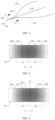
- FIG. 2 is a diagram in which an optical signal is split on an optical splitting plane 121.
- FIG. 4 is a diagram of a mode field of an optical signal before and after optical splitting.
- An optical signal is mainly transmitted in a waveguide in a form of fundamental mode, and presents a distribution manner in which energy gradually decreases from the middle to a surrounding outer side.
- a darker color corresponds to stronger optical energy.
- energy of the first optical signal in the first optical splitting waveguide 130 is different from energy of the second optical signal in the second optical splitting waveguide 140, so that optical energy finally output by the optical splitter is not equal.
- An optical splitting distance L1 of the first optical splitting waveguide 130 is less than an optical splitting distance L2 of each second optical splitting waveguide 140. In other words, the optical splitting distance L1 is less than a smaller value in the two optical splitting distances L2.
- An optical splitting distance is a distance between an energy center in the first transition waveguide 120 and an energy center in the optical splitting waveguide. In this implementation, an energy center of the first optical splitting waveguide 130 overlaps with an energy center of the first transition waveguide 120. Therefore, the optical splitting distance L1 of the first optical splitting waveguide 130 is 0, and is not shown in FIG. 2 .
- the optical splitting distance of the second optical splitting waveguide 140 is L2, and a value of the optical splitting distance L2 is greater than a value of the optical splitting distance L1.
- the optical splitting distance may alternatively be determined by measuring a gap between a central axis of the optical splitting waveguide and the center of the optical splitting plane 121.
- optical splitting distance L1 of the first optical splitting waveguide 130 is less than the optical splitting distance L2 of the second optical splitting waveguide 140.
- the optical splitting plane 121 described in this application is a plane on which one optical signal is split into a plurality of optical signals, and an input optical signal is on a side that is of the optical splitting plane 121 and that faces the optical input waveguide 110. In this case, the optical signal is not split, and there is no optical loss.
- a split optical signal is on a side that is of the optical splitting plane 121 and that faces the optical splitting waveguide. In this case, the optical signal is split into three optical signals and then enters the three optical splitting waveguides respectively. Compared with that of the optical signal before optical splitting, total energy of the optical signals after optical splitting experiences an optical energy loss, and the optical energy loss mainly occurs on a branch structure of the optical splitting plane 121.
- an optical energy proportion of the first optical splitting waveguide 130 is greater than an optical energy proportion of each second optical splitting waveguide 140, each second optical splitting waveguide 140 means every second optical splitting waveguide 140, and the optical energy proportion of the first optical splitting waveguide 130 is greater than the optical energy proportion of any second optical splitting waveguide 140.
- the first optical splitting waveguide 130 accounts for 70% of energy
- one second optical splitting waveguide 140 accounts for 15% of the energy.
- a total energy sum of one first optical splitting waveguide 130 and two second optical splitting waveguides 140 is approximately 100% (in practice, an energy loss occurs, and a total energy sum is less than 100%).
- the first optical splitting waveguide 130 with a high energy proportion is disposed between the two second optical splitting waveguides 140 with a low energy proportion.
- An optical splitting line 122 (an optical signal is split into two optical signals at the optical splitting line 122) is located in a left part region of the optical splitting plane 121, an optical energy proportion of a left side of the optical splitting line 122 is approximately 15%, the optical splitting line 122 in the left half is located in a low-energy region of the optical signal, and a branching loss is correspondingly low when optical splitting is performed herein.
- another optical splitting line 122 is located in a right part region of the optical splitting plane 121, an optical energy proportion of a right side of the optical splitting line 122 is approximately 15%, the optical splitting line 122 is located in a low-energy region of the optical signal, and a branching loss is correspondingly low when optical splitting is performed herein.
- the first optical splitting waveguide 130 is located between the plurality of second optical splitting waveguides 140, and the first connection segment 131 that is of the first optical splitting waveguide 130 and that is connected to the optical input waveguide 110 is a straight-line segment, so that an optical signal can be efficiently transmitted, and an energy loss during optical signal transmission can be reduced, to reduce an overall energy loss of the optical splitter in correspondence to and collaboration with branching loss reduction.
- the energy proportion of the first optical splitting waveguide 130 is 70%
- the energy proportion of the second optical splitting waveguide 140 is 15% in FIG. 2
- the arc-shaped waveguide and the waveguide in a straight-line shape have different optical transmission efficiency and different energy losses.
- a deviation caused by different transmission environments is taken into account.
- a specific deviation is set for a proportion of energy directly entering each branch waveguide.
- Optical energy of a middle part in FIG. 2 is approximately 70%
- optical energy of the left part and the right part in FIG. 2 is approximately 15%, to balance energy loss generated by waveguides in different shapes.
- the first optical splitting waveguide 130 in the optical splitter shown in FIG. 5 is located on one side of the two second optical splitting waveguides 140.
- One second optical splitting waveguide 140 is located between the other second optical splitting waveguide 140 and the first optical splitting waveguide 130.
- FIG. 6 is a diagram of optical energy distribution of the optical splitting plane 121 in an optical splitting waveguide distribution manner shown in FIG. 5 .
- the energy proportion of the first optical splitting waveguide 130 is 70%
- the energy proportion of one second optical splitting waveguide 140 is 15%.
- a right-side optical splitting line 122 is close to the right-side optical splitting line 122 shown in FIG.
- an optical energy proportion of a right side of the right-side optical splitting line 122 is approximately 15%.
- an optical energy proportion between a left-side optical splitting line 122 and the right-side optical splitting line 122 in FIG. 6 is approximately 15%, so that the left-side optical splitting line 122 is located in a region with higher optical signal energy, and a branching loss is higher when optical splitting is performed herein.
- the first optical splitting waveguide 130 is disposed between the two second optical splitting waveguides 140, so that the optical splitting line 122 can be effectively disposed in a low-energy region of the optical signal. This effectively reduces a branching loss of optical energy.
- the optical splitter 100 because central energy of an optical signal is high, outer side energy is low, and the center energy of the optical signal accounts for a larger proportion, when the first optical splitting waveguide 130 accounts for 70% of energy, and one second optical splitting waveguide 140 accounts for 15% of the energy, the left optical splitting line 122 and the right optical splitting line 122 are respectively located at positions at approximately one-third of the optical splitting plane 121.
- the first optical splitting waveguide 130 and the second optical splitting waveguide 140 have approximately equal cross-sectional areas, so that a cross section of the second optical splitting waveguide 140 in the optical splitting region is not to be excessively small, and manufacturing of the optical splitter 100 is more convenient.
- the first optical splitting waveguide 130 and the second optical splitting waveguide 140 have a large cross-sectional size difference, and the second optical splitting waveguide 140 in the middle has a small size, which makes it difficult to manufacture the optical splitter 100.
- Table 1 Energy table of an uneven optical splitter that includes a first optical splitting waveguide and two second optical splitting waveguides Wavelength/nm Port Energy ratio Insertion loss/dB Total energy Total loss/dB First optical splitting waveguide 69% 1.61 96.4% 0.159 1260 Second optical splitting waveguide 140a 13.7% 8.63 Second optical splitting waveguide 140b 13.7% 8.63
- the optical splitter is an optical splitter in a form of planar waveguide is used in this implementation.
- the optical splitter further includes a substrate 150, and the substrate 150 may be made of a quartz material.
- the optical input waveguide 110, the first transition waveguide 120, and the branch waveguide are waveguide paths formed in the substrate 150 by using an etching process. Specifically, cross sections of the optical input waveguide 110, the first transition waveguide 120, and the branch waveguide in this implementation are all squares, the optical input waveguide 110, the first transition waveguide 120, and the branch waveguide are all located in the substrate 150, the optical input waveguide 110 forms a light inlet (not shown in the figure) on one side of the substrate 150, and the branch waveguide forms a plurality of light output ends 160 on the other side of the substrate 150 (refer to FIG. 9 ).
- a quantity N1 of the second optical splitting waveguides 140 is an even number, and may be 2, 4, 6, 8, or the like. When N1 is 2, refer to FIG. 8 .
- Two second optical splitting waveguides 140 are respectively a second optical splitting waveguide 140a and a second optical splitting waveguide 140b, and the second optical splitting waveguide 140a and the second optical splitting waveguide 140b are respectively located on two sides of the first optical splitting waveguide 130.
- Four second optical splitting waveguides 140 are respectively the second optical splitting waveguide 140a, the second optical splitting waveguide 140b, a second optical splitting waveguide 140c, and a second optical splitting waveguide 140d.
- the four second optical splitting waveguides 140 may be evenly divided into two parts, the second optical splitting waveguide 140a and the second optical splitting waveguide 140c are located on one side of the first optical splitting waveguide 130, and the second optical splitting waveguide 140b and the second optical splitting waveguide 140d are located on the other side of the first optical splitting waveguide 130.
- the energy proportion of the first optical splitting waveguide 130 is the highest, and may be approximately 60%; energy proportions of the second optical splitting waveguide 140a and the second optical splitting waveguide 140b are lower, and may be approximately 12.5% respectively; and energy proportions of the second optical splitting waveguide 140c and the second optical splitting waveguide 140d are the lowest, and may be approximately 7.5% respectively.
- the energy proportion of the second optical splitting waveguide 140 gradually decreases along a direction away from the first optical splitting waveguide 130.
- the second optical splitting waveguides 140 may be evenly divided into two parts, and the first optical splitting waveguide 130 is located between the two parts of the evenly divided second optical splitting waveguides 140, so that the optical splitting distance L1 that is of the first optical splitting waveguide 130 and that is at the optical splitting plane 121 is less than the optical splitting distance L2 of the second optical splitting waveguide 140. This reduces an optical loss of optical splitting performed on the optical signal at the optical splitting plane 121.
- the N1 second optical splitting waveguides 140 are evenly divided into two parts, and the two parts of the second optical splitting waveguides 140 are mirror-symmetric to each other.
- the first optical splitting waveguide 130 may be a straight-line waveguide, or a section that is of the first optical splitting waveguide 130 and that is coupled to the first transition waveguide 120 is a straight-line waveguide, and the straight-line segment waveguide of the first optical splitting waveguide 130 overlaps with a mirror axis of the N1 second optical splitting waveguides 140.
- the two second optical splitting waveguides 140 are respectively the second optical splitting waveguide 140a and the second optical splitting waveguide 140b, the second optical splitting waveguide 140a and the second optical splitting waveguide 140b are respectively located on two sides of the first optical splitting waveguide 130, the first optical splitting waveguide 130 is a straight-line waveguide, and the second optical splitting waveguide 140a and the second optical splitting waveguide 140b are mirror-symmetric with respect to a straight line on which the first optical splitting waveguide 130 is located and that is used as a mirror axis.
- the second optical splitting waveguide 140a and the second optical splitting waveguide 140c are located on one side of the first optical splitting waveguide 130
- the second optical splitting waveguide 140b and the second optical splitting waveguide 140d are located on the other side of the first optical splitting waveguide 130
- the first optical splitting waveguide 130 is a straight-line waveguide.
- the second optical splitting waveguide 140a and the second optical splitting waveguide 140b are mirror-symmetric with respect to the straight line on which the first optical splitting waveguide 130 is located and that is used as the mirror axis, and transmission statuses of optical signals in the second optical splitting waveguide 140a and the second optical splitting waveguide 140b are the same.
- the second optical splitting waveguide 140c and the second optical splitting waveguide 140d are mirror-symmetric with respect to the straight line on which the first optical splitting waveguide 130 is located and that is used as the mirror axis, and transmission statuses of optical signals in the second optical splitting waveguide 140c and the second optical splitting waveguide 140d are the same.
- the optical splitter in FIG. 10 forms a 1*5 uneven optical splitter (output energy proportions may be sequentially 7.5%, 12.5%, 60%, 12.5%, and 7.5%).
- the optical splitter in this implementation may be an optical splitter in a form of fused biconical taper.
- cross sections of the optical input waveguide 110, the first transition waveguide 120, the first optical splitting waveguide 130, and the second optical splitting waveguide 140 may all be circular, there are a plurality of second optical splitting waveguides 140, and the plurality of second optical splitting waveguides 140 are sequentially spaced apart along the circumferential direction of the first optical splitting waveguide 130.
- a quantity of second optical splitting waveguides 140 is 6 is used.
- the first optical splitting waveguide 130 is disposed in a center of the branch waveguide, and the energy proportion of the first optical splitting waveguide 130 is higher than the energy proportion of the second optical splitting waveguide 140.
- a quantity of first optical splitting waveguides 130 is 1, and a quantity of second optical splitting waveguides 140 may be 3, 4, 5, or the like. In this implementation, six second optical splitting waveguides 140 are used as an example.
- the energy proportion of the first optical splitting waveguide 130 may be 70%, and the energy proportion of each second optical splitting waveguide 140 may be 5%, to form 1*7 uneven optical splitting.
- a central axis of the first optical splitting waveguide 130 overlaps with the center of the optical splitting plane 121, the optical splitting distance L1 of the first optical splitting waveguide 130 is 0, and the optical splitting distance L1 of the first optical splitting waveguide 130 is not shown in the figure.
- the optical splitting distance L2 of the second optical splitting waveguide 140 is greater than the optical splitting distance L1 of the first optical splitting waveguide 130, the first optical splitting waveguide 130 is closer to the center of the optical signal, and the first optical splitting waveguide 130 and the second optical splitting waveguide 140 perform optical splitting in a low-energy region at an edge of the optical signal, so that an optical splitting loss is lower.
- the plurality of second optical splitting waveguides 140 are sequentially spaced apart along the circumferential direction of the first optical splitting waveguide 130.
- one first optical splitting waveguide 130 and six second optical splitting waveguides 140 are used as an example.
- the first optical splitting waveguide 130 is in a straight-line shape, and the six second optical splitting waveguides 140 are of a centrosymmetric structure with respect to the straight line on which the first optical splitting waveguide 130 is located.
- the six second optical splitting waveguides 140 are of the centrosymmetric structure with respect to the straight line on which the first optical splitting waveguide 130 is located, so that transmission statuses of the optical signal entering each second optical splitting waveguide 140 after optical splitting are the same, energy proportions distributed to the second optical splitting waveguides 140 are the same, and energy output by the second optical splitting waveguides 140 is also the same.
- the second optical splitting waveguide 140 includes a second connection segment 141 and a second transmission segment 142.
- the second connection segment 141 is located between the first transition waveguide 120 and the second transmission segment 142.
- the second connection segment 141 is coupled to the first transition waveguide 120.
- the second connection segment 141 and the second transmission segment 142 may be two parts of one entire waveguide, or may be two connected waveguides.
- the second optical signal sequentially flows through the second connection segment 141 and the second transmission segment 142.
- both the second connection segment 141 and the second transmission segment 142 are arc-shaped, the second connection segment 141 bends along a transmission direction of the second optical signal toward the direction away from the first optical splitting waveguide 130, and the second transmission segment 142 bends along the transmission direction of the second optical signal toward a direction close to the first optical splitting waveguide 130.
- the second connection segment 141 and the second transmission segment 142 are tangent at a bordering position, so that when the second optical signal passes through the second connection segment 141 and the second transmission segment 142, total internal reflection can be performed on a smooth transition inner wall surface of the waveguide. This avoids an energy loss in a bordering region.
- the three optical signals respectively enter the first optical splitting waveguide 130 and the two second optical splitting waveguides 140.
- cross-sectional areas of the first optical splitting waveguide 130 and the second optical splitting waveguide 140 are small, and are mostly within a micrometer range.
- fibers need to be connected after the first optical splitting waveguide 130 and the second optical splitting waveguide 140 through corresponding interfaces, to transmit the optical signal to a back-end device.
- a size of the interface is mostly within a millimeter range. Therefore, a large gap needs to exist between the light output ends 160 of the first optical splitting waveguide 130 and the second optical splitting waveguide 140, and the second optical splitting waveguide 140 needs to be bent to a specific extent to implement a specific distance between the first optical splitting waveguide 130 and the second optical splitting waveguide 140.
- a bending radius of the waveguide should not be excessively small, and a bending degree of the waveguide should not be excessively large, to ensure that the optical signal is transmitted in the waveguide structure in a total internal reflection manner. This avoids an energy loss caused by refraction of the optical signal.
- the second optical splitting waveguide 140 in this implementation is of a double-arc-shaped structure. After the second optical splitting waveguide bends toward the side away from the first optical splitting waveguide 130, a rear side part of the second optical splitting waveguide 140 bends toward the direction close to the first optical splitting waveguide 130, to ensure that a light output direction of the second optical splitting waveguide 140 is consistent with a light output direction of the first optical splitting waveguide 130, and fibers connected to the light output side are parallel to each other. This effectively controls a size of the optical splitter and ensures reasonableness of the structure of the optical splitter.
- the second transmission segment 142 includes the light output end 160, and a light output direction of the light output end 160 is parallel to the first connection segment 131, so that after the second optical splitting waveguide 140 deviates toward two sides of the first optical splitting waveguide 130, a transmission direction of an optical signal is not changed.
- the light output end 160 is an end that is of the second transmission segment 142 and that is away from the second connection segment 141.
- the second optical splitting waveguide 140 in this implementation further includes a third transmission segment 143.
- the third transmission segment 143 is located between the second connection segment 141 and the second transmission segment 142, the third transmission segment 143 is a straight-line segment, the third transmission segment 143 and the second connection segment 141 are tangent at a connection point, and the third transmission segment 143 and the second transmission segment 142 are tangent at a connection point.
- the second connection segment 141, the second transmission segment 142, and the third transmission segment 143 may be three parts of one entire waveguide, or may be three waveguides that are sequentially connected.
- the optical splitter is a 1*9 uneven optical splitter
- a back end of the second optical splitting waveguide 140 is cascaded with a plurality of optical branching waveguides.
- a large gap needs to be reserved between the first optical splitting waveguide 130 and the second optical splitting waveguide 140, so that the plurality of branch waveguides cascaded with the back end have sufficient space to bend and there is a specific gap between a plurality of light output ends of optical signals.
- this implementation when the back end of the second optical splitting waveguide 140 can be cascaded with the plurality of optical branching waveguides, it can be ensured that the large gap exists between the second optical splitting waveguide 140 and the first optical splitting waveguide 130.
- this implementation is different from a manner in which lengths of the second connection segment 141 and the second transmission segment 142 are increased in that the third transmission segment 143 is disposed as a straight-line segment, to increase a gap between the second optical splitting waveguide 140 and the first optical splitting waveguide 130 without increasing a length of a bent part in the second optical splitting waveguide 140, so that a large energy loss caused by a long path that is of a bent waveguide and through which an optical signal passes is avoided.
- the second optical splitting waveguide 140 includes the second connection segment 141 and the second transmission segment 142.
- the second connection segment 141 is located between the first transition waveguide 120 and the second transmission segment 142.
- the second connection segment 141 is coupled to the first transition waveguide 120.
- the second connection segment 141 and the second transmission segment 142 may be two parts of one entire waveguide, or may be two connected waveguides.
- the second optical signal sequentially flows through the first transition waveguide 120, the second connection segment 141, and the second transmission segment 142.
- both the second connection segment 141 and the second transmission segment 142 are arc-shaped, the second connection segment 141 bends along the transmission direction of the second optical signal toward the direction away from the first optical splitting waveguide 130, and the second transmission segment 142 bends along the transmission direction of the second optical signal toward the direction close to the first optical splitting waveguide 130.
- a cross-sectional area of at least a section of the second connection segment 141 smoothly increases along the transmission direction of the second optical signal.
- a cross-sectional area of an overall section of the second connection segment 141 smoothly increases along the transmission direction of the second optical signal, a part that is of the second connection segment 141 and that is coupled to the first transition waveguide 120 is a thinnest part of the second connection segment 141, and a part that is of the second connection segment 141 and that is bordered to the second transmission segment 142 is a thickest part of the second connection segment 141.
- a cross-sectional area of at least a section of the second transmission segment 142 smoothly decreases along the transmission direction of the second optical signal.
- a cross-sectional area of an overall section of the second transmission segment 142 smoothly decreases along the transmission direction of the second optical signal, a part that is of the second transmission segment 142 and that is coupled to the second connection segment 141 is a thickest part of the second transmission segment 142, and the back-end light output end 160 of the second transmission segment 142 is a thinnest part of the second transmission segment 142.
- a smooth increase and smooth decrease described in this application means that in the increasing and decreasing process, the inner wall surface of the waveguide always has a smooth transition, no stepwise or disconnected increase and decrease occur, and inner wall surfaces of the second connection segment 141 and the second transmission segment 142 are smooth curved surfaces.
- Table 2 Energy distribution table of a 1*9 uneven optical splitter of a thin-thick-thin structure Wavelength/nm Port Energy ratio Port insertion loss/dB Total energy Total loss/dB 1 69% 1.61 2 3.36% 14.73 3 3.4% 14.68 4 3.21% 14.93 1260 5 3.23% 14.91 95.4% 0.213 6 3.23% 14.91 7 3.21% 14.93 8 3.4% 14.68 9 3.36% 14.73
- the second optical splitting waveguide 140 described in this implementation is of a thin-thick-thin structure.
- center deviation occurs due to reflection effect of the arc-shaped waveguide, and an energy center of the second optical signal deviates from a center of the second optical splitting waveguide 140.
- the second optical splitting waveguide 140 is disposed in the thin-thick-thin structure. As the cross-sectional area of the second optical splitting waveguide 140 increases, a center deviation degree of the second optical signal is correspondingly reduced, to improve optical splitting balance when optical splitting is performed at the back end of the second optical splitting waveguide 140.
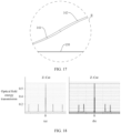
- the 1*5 uneven optical splitter in which the bent second optical splitting waveguide 140 is of the thin-thick-thin structure described in this implementation is different from an optical splitter in which a cross-sectional area of the bent second optical splitting waveguide 140 is the same in that optical energy output balance of the four even optical splitting waveguides is greatly improved, so that optical splitting balance can be effectively improved when optical splitting is performed at the back end of the second optical splitting waveguide 140.
- the optical splitter of the thin-thick-thin structure is shown in (a) in FIG. 18
- the optical splitter with the same cross-sectional area is shown in (b) in FIG. 18 .
- the second optical splitting waveguide 140 in this implementation further includes an optical branching element 144, and the second transmission segment 142 is cascaded with at least one optical branching element 144 at the light output end.
- the optical splitter may be cascaded with a plurality of levels of optical branching elements 144 at the back end of the second optical splitting waveguide 140, and the optical branching element 144 may be a 1*2 optical branching element, or may be an optical branching element such as a 1*3, 1*4, or 1*5 optical branching element. This is specifically determined based on an optical splitting ratio of the optical splitter. All second optical splitting waveguides 140 in a finally formed optical splitter have N2 second waveguide output ports 162, and N2 is an even number greater than or equal to 4.
- each second optical splitting waveguide 140 the light output end of the second transmission segment 142 of each second optical splitting waveguide 140 is cascaded with a first-level optical branching element 144, and two branch back ends of the optical branching elements 144 are cascaded with two optical branching elements 144, to form the 1*9 uneven optical splitting waveguide shown in FIG. 19 .
- the first optical splitting waveguide 130 has one first waveguide output port 161, and the second optical splitting waveguide 140 has eight second waveguide output ports 162. Optical energy output by the first waveguide output port 161 is different from optical energy output by the second waveguide output port 162, and optical energy output by the eight second waveguide output ports 162 is almost the same.
- the optical branching element 144 in this implementation may include a second transition waveguide 1441 and a plurality of optical branching waveguides 1442, a quantity of optical branching waveguides 1442 may be 2, 3, or 4, and two optical branching waveguides 1442 are used as an example in this implementation.
- the second optical signal output by the second transmission segment 142 enters the second transition waveguide 1441, and is split into a plurality of optical signals in the second transition waveguide 1441.
- the plurality of optical signals enter the optical branching waveguides 1442 in a one-to-one manner.
- the optical branching waveguide 1442 in this implementation includes a first optical splitting branch waveguide 1443, and there are two first optical splitting branch waveguides 1443.
- the first optical splitting branch waveguide 1443 is in an arc shape, and includes a first arc-shaped segment 1444 and a second arc-shaped segment 1445.
- An optical signal is sequentially transmitted through the first arc-shaped segment 1444 and the second arc-shaped segment 1445.
- the first arc-shaped segment 1444 bends along the transmission direction of the second optical signal toward a direction away from the other first optical splitting branch waveguide 1443, and the second arc-shaped segment 1445 bends along the transmission direction of the second optical signal toward a direction close to the other first optical splitting branch waveguide 1443, so that the two first optical splitting branch waveguides 1443 that are opposite to each other form a double-arc-shaped structure, and there is a specific gap between two light output ports of the first optical splitting branch waveguide 1443.
- a straight-line segment waveguide may further be added between the first arc-shaped segment 1444 and the second arc-shaped segment 1445, to increase a gap between two adjacent first optical splitting branch waveguides 1443, to ensure that a back end of the first optical splitting branch waveguide 1443 can be cascaded with another optical branching element 144.
- a cross-sectional area of at least a section of the first arc-shaped segment 1444 smoothly increases along the transmission direction of the second optical signal.
- a cross-sectional area of an overall section of the first arc-shaped segment 1444 smoothly increases along the transmission direction of the second optical signal, a part that is of the first arc-shaped segment 1444 and that is coupled to the second transition waveguide 1441 is a thinnest part of the first arc-shaped segment 1444, and a part that is of the first arc-shaped segment 1444 and that is bordered to the second arc-shaped segment 1445 is a thickest part of the first arc-shaped segment 1444.
- a cross-sectional area of at least a section of the second arc-shaped segment 1445 smoothly decreases along the transmission direction of the second optical signal.
- a cross-sectional area of an overall section of the second arc-shaped segment 1445 smoothly decreases along the transmission direction of the second optical signal, a part that is of the second arc-shaped segment 1445 and that is bordered to the first arc-shaped segment 1444 is a thickest part of the second arc-shaped segment 1445, and the light output end 160 at the back end of the second arc-shaped segment 1445 is a thinnest part of the second arc-shaped segment 1445.
- the first optical splitting branch waveguide 1443 described in this implementation is of a thin-thick-thin structure.
- center deviation occurs due to reflection effect of the arc-shaped waveguide, and a center of the second optical signal deviates from a center of the first optical splitting branch waveguide 1443.
- a deviation degree is more obvious.
- the first optical splitting branch waveguide 1443 is disposed in the thin-thick-thin structure, so that a quantity of reflection times of the second optical signal in the first optical splitting branch waveguide 1443 can be reduced.
- a center deviation degree of the second optical signal is correspondingly reduced, to improve optical splitting balance when optical splitting is performed at the back end of the second optical splitting waveguide 140.
- the optical branching waveguide 1442 further includes a second optical splitting branch waveguide 1446, and the second optical splitting branch waveguide 1446 is located between the two first optical splitting branch waveguides 1443.
- the second optical splitting branch waveguide 1446 may be in a straight-line shape as a whole, or a section that is of the second optical splitting branch waveguide 1446 and that is coupled to the second transition waveguide 1441 is in a straight-line shape, and a section at the back end is a nonlinear waveguide such as an arc-shaped waveguide or a staggered waveguide.
- the optical splitter chip includes the optical splitter 100 according to any one of the foregoing implementations.
- the first optical splitting waveguide 130 and the second optical splitting waveguide 140 in the optical splitter 100 are coplanar, and the plurality of second optical splitting waveguides 140 are divided into two parts and located on two sides of the first optical splitting waveguide 130.
- the optical splitter chip further includes the substrate 150.
- the substrate 150 may be made of a quartz material.
- the optical input waveguide 110, the first transition waveguide 120, and the branch waveguide are waveguide paths formed in the substrate 150 by using an etching process. Specifically, cross sections of the optical input waveguide 110, the first transition waveguide 120, and the branch waveguide in this implementation are all squares, the optical input waveguide 110, the first transition waveguide 120, and the branch waveguide are all located in the substrate 150, the optical input waveguide 110 forms the light inlet (not shown in the figure) on one side of the substrate 150, and the branch waveguide forms the plurality of light output ends 160 on the other side of the substrate 150 (refer to FIG. 9 ).
- a quantity N1 of the second optical splitting waveguides 140 is an even number, and may be 2, 4, 6, 8, or the like. When N1 is 2, refer to FIG. 8 .
- Two second optical splitting waveguides 140 are respectively the second optical splitting waveguide 140a and the second optical splitting waveguide 140b, and the second optical splitting waveguide 140a and the second optical splitting waveguide 140b are respectively located on two sides of the first optical splitting waveguide 130.
- Four second optical splitting waveguides 140 are respectively the second optical splitting waveguide 140a, the second optical splitting waveguide 140b, the second optical splitting waveguide 140c, and the second optical splitting waveguide 140d.
- the four second optical splitting waveguides 140 may be evenly divided into two parts, the second optical splitting waveguide 140a and the second optical splitting waveguide 140c are located on one side of the first optical splitting waveguide 130, and the second optical splitting waveguide 140b and the second optical splitting waveguide 140d are located on the other side of the first optical splitting waveguide 130.
- the energy proportion of the first optical splitting waveguide 130 is the highest, and may be approximately 60%; energy proportions of the second optical splitting waveguide 140a and the second optical splitting waveguide 140b are lower, and may be approximately 12.5% respectively; and energy proportions of the second optical splitting waveguide 140c and the second optical splitting waveguide 140d are the lowest, and may be approximately 7.5% respectively.
- the energy proportion of the second optical splitting waveguide 140 gradually decreases along the direction away from the first optical splitting waveguide 130.
- the second optical splitting waveguides 140 may be evenly divided into two parts, and the first optical splitting waveguide 130 is located between the two parts of the evenly divided second optical splitting waveguides 140, so that the optical splitting distance L1 that is of the first optical splitting waveguide 130 and that is at the optical splitting plane 121 is less than the optical splitting distance L2 of the second optical splitting waveguide 140. This reduces an optical loss of optical splitting performed on the optical signal at the optical splitting plane 121.
- the communication device includes the optical splitter 100 according to any one of the foregoing implementations, and further includes an optical line terminal 200.
- the optical line terminal 200 is connected to the optical input waveguide 110 of the optical splitter 100 through a trunk fiber 210, and the optical line terminal 200 is configured to input an optical signal to the optical input waveguide 110.
- the optical line terminal 200 and the optical splitter 100 may be integrated into one device, and optical signal connection is implemented inside the device through the trunk fiber 210.
- a plurality of output ports of the optical splitter 100 are configured to connect to the optical network unit 300, to implement optical signal transmission and distribution.
- the optical distribution network includes the optical splitter 100 according to any one of the foregoing implementations, and further includes an optical line terminal 200 and a plurality of optical network units 300.
- the optical line terminal 200 is coupled to the optical input waveguide 110 of the optical splitter 100 through the trunk fiber 210.
- the optical line terminal 200 is configured to input an optical signal to the optical input waveguide 110.
- the plurality of optical network units 300 are coupled to output ports of the optical splitter 100 in a one-to-one manner through branch fibers 310.
- An optical splitter is a passive device for FTTH access. It is generally used by operators in the communication industry to branch broadband on a home broadband side. Specifically, the optical splitter may be used in a passive optical network (passive optical network, PON) system, and the system generally includes an optical line terminal (optical Line Terminal, OLT), an optical distribution network (optical distribution network, ODN), and an optical network unit (optical network unit, ONU).
- OLT optical Line Terminal
- ODN optical distribution network
- ONU optical network unit
- the ODN provides an optical transmission physical channel between the OLT and the ONU.
- the PON system in this embodiment of this application may be a next-generation PON (next-generation PON, NGPON), an NG-PON1, an NG-PON2, a gigabit-capable PON (gigabit-capable PON, GPON), a 10 gigabit per second PON (10 gigabit per second PON, XG-PON), a 10-gigabit-capable symmetric passive optical network (10-gigabit-capable symmetric passive optical network, XGS-PON), an Ethernet PON (Ethernet PON, EPON), a 10 gigabit EPON (10 gigabit per second EPON, 10G-EPON), a next-generation EPON (next-generation EPON, NG-EPON), wavelength-division multiplexing (wavelength-division multiplexing, WDM) PON, time and wavelength-division multiplexing (time and wavelength-division multiplexing, TWDM) PON, point-to-point (point-to-point
- a direction from the OLT to the ONU is defined as a downlink direction
- a direction from the ONU to the OLT is defined as an uplink direction.
- the OLT is a core component of an optical access network, and is usually located in a central office (Central Office, CO), and may manage at least one ONU in a unified manner.
- the OLT is configured to provide data for each accessed ONU, provide management, and the like.
- the OLT may be configured to send an optical signal to each ONU, receive information fed back by each ONU, and process the information fed back by the ONU, other data, or the like.
- the ONU is configured to receive data sent by the OLT, respond to a management command of the OLT, cache Ethernet data of a user, send data in the uplink direction in a transmit window allocated by the OLT, and so on.
- the ODN generally includes an optical distribution frame (Optical Distribution Frame, ODF), a fiber splice closure (also referred to as a splitting and splicing closure (splitting and splicing closure, SSC)), a fiber optical distribution box (also referred to as a fiber distribution terminal (FDT)), a fiber splitter box (also referred to as a fiber access terminal (fiber access terminal, FAT)), a fiber terminal closure (also referred to as an access terminal box (access terminal box, ATB)), and the like.
- the FDT may include an optical splitter A
- the FAT may include an optical splitter B.
- An optical signal from the OLT is sequentially split by the ODF, the SSC, the optical splitter A in the FDT, and the optical splitter B in the FAT, and reaches the ONU through the ATB.
- the optical signal from the OLT is transmitted to the ONU through an optical link between the OLT and the ONU.
- the optical splitter A equally divides power of a received optical signal, and one of the optical signal is transmitted to the optical splitter B through one branch.
- the optical splitter B equally divides power of the received optical signal, and the optical signal is separately transmitted to the connected ONU through each branch.
- An output end of a last-level optical splitter in the ODN is used as an output port of the ODN, and the ONU is connected to the output port of the ODN.
- there are a plurality of optical splitters 100 in the optical distribution network a part of the plurality of optical splitters 100 are level-1 optical splitters, another part of the plurality of optical splitters 100 are level-2 optical splitters, an input port of the level-2 optical splitter is connected to an output port of the level-1 optical splitter, and the output port is an output port of the first optical splitting waveguide and/or an output port of the second optical splitting waveguide.
Landscapes
- Physics & Mathematics (AREA)
- General Physics & Mathematics (AREA)
- Optics & Photonics (AREA)
- Engineering & Computer Science (AREA)
- Microelectronics & Electronic Packaging (AREA)
- Optical Integrated Circuits (AREA)
Applications Claiming Priority (2)
| Application Number | Priority Date | Filing Date | Title |
|---|---|---|---|
| CN202211071396.XA CN117687144A (zh) | 2022-09-02 | 2022-09-02 | 分光器、分光器芯片、通信设备和光分配网 |
| PCT/CN2023/115600 WO2024046331A1 (zh) | 2022-09-02 | 2023-08-29 | 分光器、分光器芯片、通信设备和光分配网 |
Publications (2)
| Publication Number | Publication Date |
|---|---|
| EP4567480A1 true EP4567480A1 (de) | 2025-06-11 |
| EP4567480A4 EP4567480A4 (de) | 2025-11-12 |
Family
ID=90100386
Family Applications (1)
| Application Number | Title | Priority Date | Filing Date |
|---|---|---|---|
| EP23859360.2A Pending EP4567480A4 (de) | 2022-09-02 | 2023-08-29 | Optischer splitter, optischer splitterchip, kommunikationsvorrichtung und optisches verteilungsnetzwerk |
Country Status (4)
| Country | Link |
|---|---|
| US (1) | US20250231343A1 (de) |
| EP (1) | EP4567480A4 (de) |
| CN (1) | CN117687144A (de) |
| WO (1) | WO2024046331A1 (de) |
Family Cites Families (20)
| Publication number | Priority date | Publication date | Assignee | Title |
|---|---|---|---|---|
| NL9400993A (nl) * | 1994-06-17 | 1996-02-01 | Nederland Ptt | Polarisatie- en golflengte-onafhankelijk optisch vermogen splitsend circuit. |
| DE19630706A1 (de) * | 1996-07-30 | 1998-02-05 | Deutsche Telekom Ag | Optischer Verzweiger |
| KR19990038490A (ko) * | 1997-11-05 | 1999-06-05 | 윤종용 | 광파워 분할기 및 그 제작방법 |
| JP2000231026A (ja) * | 1998-12-08 | 2000-08-22 | Showa Electric Wire & Cable Co Ltd | 光導波路型光分岐合波回路 |
| US6810167B2 (en) * | 2001-10-29 | 2004-10-26 | Fujitsu Limited | Wavelength division demultiplexing apparatus |
| WO2005103775A1 (ja) * | 2004-04-19 | 2005-11-03 | Hitachi Chemical Company, Ltd. | S字型曲線光導波路及び光学装置 |
| JP2005189385A (ja) * | 2003-12-25 | 2005-07-14 | Sony Corp | 分岐型光導波路、光源モジュール、並びに光情報処理装置 |
| JP2005266381A (ja) * | 2004-03-19 | 2005-09-29 | Nec Corp | 導波路型光スプリッタ及びこれを備えた導波路型光モジュール |
| KR200363965Y1 (ko) * | 2004-07-01 | 2004-10-08 | 우리로광통신주식회사 | 3분기형 광 도파로 |
| JP2006099009A (ja) * | 2004-09-30 | 2006-04-13 | Sanyo Electric Co Ltd | 光分岐デバイス及び光カプラモジュール |
| JP2006293171A (ja) * | 2005-04-13 | 2006-10-26 | Matsushita Electric Works Ltd | 光分岐回路 |
| JP2006317545A (ja) * | 2005-05-10 | 2006-11-24 | Hitachi Chem Co Ltd | 光導波路構造 |
| JP2006323019A (ja) * | 2005-05-17 | 2006-11-30 | Matsushita Electric Works Ltd | 多分岐光回路 |
| CN201177670Y (zh) * | 2007-05-25 | 2009-01-07 | 江苏大学 | 激模波导结构三分支光分路器 |
| KR101066544B1 (ko) * | 2009-07-29 | 2011-09-21 | 우리로광통신주식회사 | 광 분배기 |
| JP6676964B2 (ja) * | 2015-12-25 | 2020-04-08 | 株式会社豊田中央研究所 | 光導波路 |
| CN110794514A (zh) * | 2019-11-18 | 2020-02-14 | 上海鸿辉光通科技股份有限公司 | 一种非均分光分路器及其制备方法 |
| EP3926233B1 (de) * | 2020-06-19 | 2024-07-17 | VitreaLab GmbH | Optische vorrichtung |
| CN114594554A (zh) * | 2020-12-04 | 2022-06-07 | 青岛海信宽带多媒体技术有限公司 | 一种光模块 |
| CN219122452U (zh) * | 2022-09-02 | 2023-06-02 | 华为技术有限公司 | 分光器、分光器芯片、通信设备和光分配网 |
-
2022
- 2022-09-02 CN CN202211071396.XA patent/CN117687144A/zh active Pending
-
2023
- 2023-08-29 WO PCT/CN2023/115600 patent/WO2024046331A1/zh not_active Ceased
- 2023-08-29 EP EP23859360.2A patent/EP4567480A4/de active Pending
-
2025
- 2025-02-28 US US19/067,233 patent/US20250231343A1/en active Pending
Also Published As
| Publication number | Publication date |
|---|---|
| EP4567480A4 (de) | 2025-11-12 |
| CN117687144A (zh) | 2024-03-12 |
| US20250231343A1 (en) | 2025-07-17 |
| WO2024046331A1 (zh) | 2024-03-07 |
Similar Documents
| Publication | Publication Date | Title |
|---|---|---|
| US11644619B2 (en) | Optical splitter chip, optical splitter component, optical splitter apparatus, and optical fiber box | |
| CN103765265B (zh) | 光合路分路器、双向光传播器以及光发送接收系统 | |
| JP2953947B2 (ja) | 光通信ネットワーク | |
| US9354396B2 (en) | Large bandwidth multi-mode interference device | |
| CN106576000B (zh) | 分光器、信号传输方法和无源光网络 | |
| US6012855A (en) | Method and apparatus for parallel optical data link | |
| US9910218B2 (en) | Optical module and optical network system | |
| JP4010012B2 (ja) | 光導波路を含む光システム | |
| CN114721092A (zh) | 一种功率分配器以及光纤通信系统 | |
| CN219122452U (zh) | 分光器、分光器芯片、通信设备和光分配网 | |
| EP4567480A1 (de) | Optischer splitter, optischer splitterchip, kommunikationsvorrichtung und optisches verteilungsnetzwerk | |
| EP4141502A1 (de) | Diffraktionskompensierte kompakte wellenlängenmultiplexvorrichtungen | |
| US20240069286A1 (en) | Dual Layer Optical Coupling Configuration Between Photonic Integrated Circuit And External Single Mode Optical Fiber | |
| US9151914B2 (en) | Optical communication systems and methods for minimizing reflective feedback | |
| KR101501140B1 (ko) | 광 파워 모니터 구조를 개량시킨 평판형 광도파로 소자 모듈 | |
| CN110475164B (zh) | 光分路器及单纤双向无源光网络传输系统 | |
| CN105938223A (zh) | 低损耗四端口混合型两波长波分复用光无源器件 | |
| US20250167911A1 (en) | Efficient higher loss budget pon transceiver | |
| JPH06313821A (ja) | オプトエレクトロニク集積回路 | |
| CN114200684B (zh) | 一种分光器以及通信系统 | |
| US12301287B2 (en) | Loss optimizing asymmetric optical splitter | |
| CN215728932U (zh) | 一种光学器件 | |
| Du et al. | Optimization Design of Arrayed Waveguide Grating Using Dual-Etched Multimode Interference Aperture | |
| Arao et al. | Single-mode 32-fiber connector with GI fiber lens array | |
| Oki et al. | Development of Small Receiver Module with Integrated Optical Demultiplexer |
Legal Events
| Date | Code | Title | Description |
|---|---|---|---|
| STAA | Information on the status of an ep patent application or granted ep patent |
Free format text: STATUS: THE INTERNATIONAL PUBLICATION HAS BEEN MADE |
|
| PUAI | Public reference made under article 153(3) epc to a published international application that has entered the european phase |
Free format text: ORIGINAL CODE: 0009012 |
|
| STAA | Information on the status of an ep patent application or granted ep patent |
Free format text: STATUS: REQUEST FOR EXAMINATION WAS MADE |
|
| 17P | Request for examination filed |
Effective date: 20250306 |
|
| AK | Designated contracting states |
Kind code of ref document: A1 Designated state(s): AL AT BE BG CH CY CZ DE DK EE ES FI FR GB GR HR HU IE IS IT LI LT LU LV MC ME MK MT NL NO PL PT RO RS SE SI SK SM TR |
|
| A4 | Supplementary search report drawn up and despatched |
Effective date: 20251014 |
|
| RIC1 | Information provided on ipc code assigned before grant |
Ipc: G02B 6/12 20060101AFI20251008BHEP Ipc: G02B 6/125 20060101ALI20251008BHEP |
|
| DAV | Request for validation of the european patent (deleted) | ||
| DAX | Request for extension of the european patent (deleted) |