EP4567842A1 - Circuit pour actionner un actionneur lineaire electromagnetique - Google Patents
Circuit pour actionner un actionneur lineaire electromagnetique Download PDFInfo
- Publication number
- EP4567842A1 EP4567842A1 EP23214312.3A EP23214312A EP4567842A1 EP 4567842 A1 EP4567842 A1 EP 4567842A1 EP 23214312 A EP23214312 A EP 23214312A EP 4567842 A1 EP4567842 A1 EP 4567842A1
- Authority
- EP
- European Patent Office
- Prior art keywords
- switching element
- electrical energy
- circuit arrangement
- input
- linear drive
- Prior art date
- Legal status (The legal status is an assumption and is not a legal conclusion. Google has not performed a legal analysis and makes no representation as to the accuracy of the status listed.)
- Pending
Links
Images

Classifications
-
- H—ELECTRICITY
- H01—ELECTRIC ELEMENTS
- H01F—MAGNETS; INDUCTANCES; TRANSFORMERS; SELECTION OF MATERIALS FOR THEIR MAGNETIC PROPERTIES
- H01F7/00—Magnets
- H01F7/06—Electromagnets; Actuators including electromagnets
- H01F7/064—Circuit arrangements for actuating electromagnets
-
- H—ELECTRICITY
- H01—ELECTRIC ELEMENTS
- H01F—MAGNETS; INDUCTANCES; TRANSFORMERS; SELECTION OF MATERIALS FOR THEIR MAGNETIC PROPERTIES
- H01F7/00—Magnets
- H01F7/06—Electromagnets; Actuators including electromagnets
- H01F7/08—Electromagnets; Actuators including electromagnets with armatures
- H01F7/18—Circuit arrangements for obtaining desired operating characteristics, e.g. for slow operation, for sequential energisation of windings, for high-speed energisation of windings
- H01F7/1805—Circuit arrangements for holding the operation of electromagnets or for holding the armature in attracted position with reduced energising current
- H01F7/1811—Circuit arrangements for holding the operation of electromagnets or for holding the armature in attracted position with reduced energising current demagnetising upon switching off, removing residual magnetism
-
- H—ELECTRICITY
- H01—ELECTRIC ELEMENTS
- H01F—MAGNETS; INDUCTANCES; TRANSFORMERS; SELECTION OF MATERIALS FOR THEIR MAGNETIC PROPERTIES
- H01F7/00—Magnets
- H01F7/06—Electromagnets; Actuators including electromagnets
- H01F7/08—Electromagnets; Actuators including electromagnets with armatures
- H01F7/18—Circuit arrangements for obtaining desired operating characteristics, e.g. for slow operation, for sequential energisation of windings, for high-speed energisation of windings
- H01F7/1805—Circuit arrangements for holding the operation of electromagnets or for holding the armature in attracted position with reduced energising current
- H01F7/1816—Circuit arrangements for holding the operation of electromagnets or for holding the armature in attracted position with reduced energising current making use of an energy accumulator
-
- H—ELECTRICITY
- H01—ELECTRIC ELEMENTS
- H01F—MAGNETS; INDUCTANCES; TRANSFORMERS; SELECTION OF MATERIALS FOR THEIR MAGNETIC PROPERTIES
- H01F7/00—Magnets
- H01F7/06—Electromagnets; Actuators including electromagnets
- H01F2007/062—Details of terminals or connectors for electromagnets
-
- H—ELECTRICITY
- H01—ELECTRIC ELEMENTS
- H01F—MAGNETS; INDUCTANCES; TRANSFORMERS; SELECTION OF MATERIALS FOR THEIR MAGNETIC PROPERTIES
- H01F7/00—Magnets
- H01F7/06—Electromagnets; Actuators including electromagnets
- H01F7/08—Electromagnets; Actuators including electromagnets with armatures
- H01F7/18—Circuit arrangements for obtaining desired operating characteristics, e.g. for slow operation, for sequential energisation of windings, for high-speed energisation of windings
- H01F7/1805—Circuit arrangements for holding the operation of electromagnets or for holding the armature in attracted position with reduced energising current
- H01F7/1816—Circuit arrangements for holding the operation of electromagnets or for holding the armature in attracted position with reduced energising current making use of an energy accumulator
- H01F2007/1822—Circuit arrangements for holding the operation of electromagnets or for holding the armature in attracted position with reduced energising current making use of an energy accumulator using a capacitor to produce a boost voltage
Definitions
- the invention relates to a circuit arrangement for actuating an electromagnetic linear actuator.
- Electromagnetic linear actuators are used, for example, to actuate valves, relays, contactors, and the like.
- An electromagnetic linear drive within the meaning of the invention is an electrically operated motor with a stator and an armature movably mounted on the stator such that the armature can move translationally relative to the stator, i.e., can be displaced along a mostly straight line.
- the armature can be elastically preloaded into a rest position of the armature by means of a spring fixed in position relative to the stator. In the rest position, the armature is usually arranged partially outside the stator or next to the stator with respect to a direction of movement of the stator.
- a maximum length of the translational movement between the rest position and a working position of the armature is referred to as a stroke of the electromagnetic linear drive.
- the stator and the armature can each comprise electromagnets or a soft magnetic, particularly ferromagnetic, material.
- Each electromagnet typically comprises an electrical coil with self-inductance.
- the electrical coil comprises an electrical conductor, for example, a copper wire wound in a plurality of turns.
- the electrical coil of the electromagnetic linear actuator can comprise a plurality of windings.
- the electric coil When an electric current flows in the electric coil, the electric coil generates a magnetic field and magnetizes the soft magnetic core of the armature, thereby subjecting the armature to a force and accelerating it in the constant magnetic field provided by the electric coil. If the armature is elastically preloaded into the rest position by a spring, the armature is accelerated from the rest position against the elastic restoring force of the spring.
- the electromagnetic linear actuator is operated by means of a suitable circuit arrangement.
- the circuit arrangement connects the electromagnetic linear actuator to an electrical voltage source, which provides an electrical potential difference, referred to as the supply voltage, for operating the electromagnetic linear actuator.
- the circuit arrangement comprises at least one electronically controllable switching element for selectively connecting and disconnecting the electromagnetic linear drive to or from the voltage source and may comprise a plurality of additional electronic components.
- a switching element, or switch for short, is electronically controllable if it enables actuation by means of an electrical signal, and in particular, automatic actuation.
- a normal operating cycle of an electromagnetic linear actuator can be divided into four phases: a pull-in phase until the armature leaves the rest position, a flight phase during which the armature moves from the rest position to the working position, a holding phase during which the armature remains in the working position, and a release phase during which the armature moves back to the rest position.
- a pull-in phase until the armature leaves the rest position
- a flight phase during which the armature moves from the rest position to the working position
- a holding phase during which the armature remains in the working position
- a release phase during which the armature moves back to the rest position.
- the electromagnetic linear actuator is connected to the supply voltage of a voltage source, i.e. an electrical potential difference
- the electric coil is electrically connected to the voltage source by closing at least one electronically controllable switching element.
- An electric current then flowing through the electric coil generates an induced voltage by means of self-induction in the electric coil.
- This induced voltage is polarized opposite to the supply voltage according to Lenz's law and counteracts the electric current. Due to the induced voltage, the electric current does not increase abruptly, but rather steadily.
- the armature When the magnetic field generated by the coil reaches a minimum strength, the armature leaves the rest position, and the electromagnetic linear actuator enters the flight phase.
- the minimum strength can be defined by the elastic restoring force of a spring.
- the strength of the generated magnetic field continues to increase asymptotically until it reaches a maximum strength.
- the armature finally reaches the working position. The armature, advancing toward the stator, increases the self-inductance of the electric coil.
- the holding phase can begin, during which the armature remains in the operating position and the strength of the generated magnetic field is maintained, compensating for ohmic losses in the electrical coil.
- the magnetic field generated by the electrical coil during the holding phase stores electrical energy.
- a spring deflected in the holding position can store mechanical energy.
- the electromagnetic linear drive is disconnected from the supply voltage, which initiates the final decay phase.
- the electrical coil provides an induction voltage that is polarized opposite to the supply voltage according to Lenz's law. Due to the increased self-inductance of the electrical coil in the operating position, the induction voltage can be so high that the voltage required to disconnect the electromagnetic linear drive from the power source used electronically controllable switching element is damaged or destroyed, for example by means of an electrical breakdown or a switching spark or a switching arc.
- the circuit arrangement can include an electronic valve that connects the terminals of the electrical coil.
- An electronic valve is understood here and below to be an electronic component that usually includes at least one pn junction and can prevent current flow through the electronic component in a voltage-dependent manner.
- diodes, bidirectional diodes, and varistors are electronic valves within the meaning of the invention.
- a bidirectional diode is also referred to as a DIAC (diode for alternating current).
- a diode consists of exactly two oppositely doped semiconductor regions, known as a pn junction.
- the pn junction allows current to flow in a forward direction above a so-called threshold voltage and prevents current flow in a reverse direction opposite to the forward direction below a so-called breakdown voltage.
- a varistor is a voltage-dependent resistor that prevents current flow in any direction below a so-called varistor voltage and allows it above the varistor voltage.
- a diode as an electronic valve is arranged in the reverse direction with respect to the supply voltage and only provides a short circuit to the electrical coil for an electrical current flowing against the supply voltage. Due to the self-induction of the electrical coil, the electrical current flowing through the electronic valve does not decrease abruptly, but rather steadily and exponentially. The energy stored in the electromagnetic linear actuator is thus essentially transformed into ohmic heat loss by the electrical coil and remains unused.
- the magnetic field generated by the electric coil does not decrease abruptly, but rather steadily and exponentially.
- the return of the armature from the working position to the rest position, and thus the subsequent activation of the circuit arrangement for actuating an electromagnetic linear actuator is delayed.
- the ohmic heat loss generated during each cycle of the electromagnetic linear actuator can impede a rapid cycle sequence.
- the supply input and the ground input form in particular an input side of the circuit arrangement for connecting the DC voltage source.
- the load output and the ground output form in particular an output side of the circuit arrangement for connecting the electromagnetic linear drive.
- the supply input, the ground input, the load output and the ground output serve to define the circuit arrangement and can be physically designed as connection contacts. However, it is also conceivable that these are merely imaginary points in the respective lines.
- the first switching element and the second switching element enable the outputs of the circuit arrangement to be separated from the inputs of the circuit arrangement.
- the switching elements allow the electromagnetic linear drive to be completely disconnected from the DC voltage source.
- the control unit is configured to operate the first electronically controllable switching element and the second electronically controllable switching element synchronously, i.e., to open and close them simultaneously.
- the circuit arrangement according to the invention comprises a first electronic valve connecting the load output to the ground input and a second electronic valve connecting the ground output to an input side of the first switching element, which each provide electrical connections from the second pole of the electromagnetic linear drive to the ground input and from the first pole of the electromagnetic linear drive to the input side of the first switching element in order to conduct an induction current induced in the electromagnetic linear drive after opening of the electronically controllable switching elements.
- the first electronic The valve and the second electronic valve are designed, for example, as diodes or varistors and are configured and arranged to block a current provided by the DC voltage source—in short, the supply current.
- the electronic valves do not generate a short circuit when the electronically controllable switching elements are closed, i.e., during the pull-in phase, the flight phase, and the holding phase of the electromagnetic linear drive.
- the supply current flows, in particular, from one pole of the DC voltage source through the closed switching elements and the electromagnetic linear drive to the other pole.
- the electronic valves allow the induction current to flow out of the electromagnetic linear actuator, particularly during the decay phase, thus preventing harmful overvoltage and making it possible to utilize the energy stored in the electromagnetic linear actuator, i.e. electrical energy of the magnetic field and, if applicable, mechanical energy of the spring.
- the electronic valves connect the ground output to the supply input, and the load output to the ground input.
- the electronically controllable switching elements are opened, the induced current flows into the DC power source.
- the energy stored in the electromagnetic linear actuator is fed into the DC power source and is not lost as ohmic heat.
- the circuit arrangement may comprise an electrical energy storage device connected to the ground input and the second electronic valve, which is charged by the induced induction current.
- the electrical energy storage device is advantageously designed to be charged by the induction current, i.e., to absorb the energy stored in the electromagnetic linear drive after the holding phase and store it for later use.
- the electrical energy storage device and the second electronic valve are connected to the supply input.
- the DC voltage source can precharge the electrical energy storage device at least substantially to a supply voltage provided by the DC voltage source.
- the electrical lines between the supply input and the electrical energy storage device and between the ground input and the electrical energy storage device, as well as any other electronic components through which a precharging current provided by the DC voltage source flows, can be referred to as a precharging circuit of the voltage arrangement.
- Precharging refers to the charging of the electrical energy storage device using an electrical charging current provided by the DC voltage source.
- the precharged energy storage device shortens the pull-in phase that begins with the closing of the electronically controllable switching elements and improves the response of the electromagnetic linear drive. In particular, heating of the circuit arrangement is prevented or at least reduced.
- the circuit arrangement advantageously includes a third electronic valve connecting the supply input to the electrical energy storage device.
- the third electronic valve enables a charging voltage of the electrical energy storage device that is higher than the supply voltage provided by the DC voltage source.
- the circuit arrangement comprises a DC/DC converter with an input connected to the electrical energy storage device and an output for connecting a further electronic circuit.
- the DC/DC converter converts an electrical voltage provided by the energy storage device into an electrical operating voltage required by the further electronic circuit. In this way, proper operation of the further electronic circuit is enabled regardless of the electrical voltage supplied by the electrical Energy storage is provided.
- the combination of the DC/DC converter and the additional electronic circuit can be referred to as a discharge circuit of the circuit arrangement.
- a further circuit arrangement for actuating an electromagnetic linear drive comprises a ground input for connecting a negative pole of a DC voltage source, a ground output connected to the ground input for connecting a first pole of the electromagnetic linear drive, a supply input for connecting a positive pole of the DC voltage source, a load output for connecting a second pole of the electromagnetic linear drive, a first, in particular electronically controllable, switching element for selectively disconnecting and connecting the load output from the supply input, wherein the first switching element is to be opened to disconnect the load output from the supply input, and a control unit connected to a control input of the first switching element for controlling the first switching element.
- the circuit arrangement does not include a second electronically controllable switching element.
- the ground output and the second pole of the electromagnetic linear drive are permanently electrically connected.
- the electromagnetic linear drive is not potential-free, which offers advantages in terms of circuitry and/or measurement technology.
- the circuit arrangement comprises an electrical energy store, a first electronic valve connecting the electrical energy store to the load output, which first electronic valve allows further charging of the electrical energy store with an induction current induced in the electromagnetic linear drive, and a pre-charging and discharging circuit for pre-charging and discharging the electrical energy store to a supply voltage provided by the DC voltage source, wherein the electrical energy store is connected to the electromagnetic linear drive in such a way can be connected such that, after the first switching element is opened, the induction current induced in the electromagnetic linear drive is conducted to the electrical energy storage device and further charges it.
- the pre-charging and discharging circuit ensures that, before the first electronically controllable switching element is closed, the electrical energy storage device is pre-charged to the supply voltage using a charging current provided by the DC voltage source. Pre-charging the electrical energy storage device improves the responsiveness of the electromagnetic linear drive. By continuing to charge, the electrical energy storage device is further charged after pre-charging.
- the pre-discharge and discharge circuit also ensures that the electrical energy storage device is discharged to the supply voltage after the first electronically controllable switching element is opened.
- a discharge current provided by the electrical energy storage device can flow through the pre-discharge and discharge circuit into the DC voltage source. This prevents harmful overvoltage during the decay phase of the electromagnetic linear drive.
- the energy stored in the electromagnetic linear drive is fed into the DC power source and is not lost as heat due to ohmic losses.
- the circuit arrangement preferably comprises a plurality of electronically controllable first switching elements, load outputs, and first electronic valves.
- the circuit arrangement can operate a plurality of electromagnetic linear drives independently of one another.
- the second poles of the electromagnetic linear drives are connected to the ground output of the circuit arrangement and are at the same electrical potential.
- the first pole of each electromagnetic linear drive is connected to exactly one load output.
- the electrical energy storage device of the pre-discharge and discharge circuit is designed to absorb the stored energy of all electromagnetic linear drives during respective decay phases and to release it again during discharging in order to feed it into the DC voltage source.
- the circuit arrangement may also comprise at least one second electronic valve which connects the ground output to the energy storage device and allows further charging of the electrical energy storage device with the induction current induced in the electromagnetic linear drive.
- the pre-discharge and discharge circuit comprises a bidirectional charge pump that provides the electrical energy storage device, which is connected to the ground input, the ground output, and the first electronic valve connected to the load output.
- the bidirectional charge pump is advantageously designed to transport, i.e., pump, electrical energy from the DC voltage source to the electrical energy storage device or from the electrical energy storage device to the DC voltage source. The transport preferably takes place in multiple steps and periodically.
- the bidirectional charge pump comprises an additional electrical energy storage device for charging and discharging the electrical energy storage device.
- the additional electrical energy storage device acts as an intermediate storage device for the electrical energy transported bidirectionally between the DC voltage source and the electrical energy storage device.
- the pre-discharge and discharge circuit can comprise at least one third electronically controllable switching element with a control input connected to the control unit, via which the electrical energy storage device can be pre-charged or discharged to the voltage provided by the DC voltage source.
- Each third electronically controllable switching element serves to start and end a pumping step.
- several, in particular four, third electronically controllable switching elements can be opened and closed in pairs synchronously and alternately to start or end a pumping step.
- the pre-discharge and discharge circuit comprises at least one coil, a second electronic valve, and/or a pre-charging resistor, via which the electrical energy storage device can be pre-charged.
- the at least one coil can reduce ohmic losses during pumping.
- the second electronic valve and/or the precharge resistor may belong to a precharge and discharge circuit separate from the bidirectional charge pump.
- the precharge resistor may limit a precharge current provided by the DC voltage source.
- the precharge and discharge circuit may comprise a plurality of precharge resistors.
- At least one of the electrical energy storage devices is designed as a capacitor.
- the capacitor is very well suited for storing electrical energy. Capacitors with different capacitances are available, so that the capacitor can be selected to match the electromagnetic linear drive.
- the electrical energy storage device can comprise a plurality of capacitors, in particular in a parallel circuit.
- Any electronically controllable switching element can be a bipolar transistor, IGBT, field-effect transistor (FET), thyristor, or relay.
- the IGBT is a bipolar transistor with an insulated-gate electrode (insulated-gate bipolar transistor).
- Bipolar transistors can switch higher currents than conventional transistors.
- the thyristor comprises four or more semiconductor layers with alternating doping. While in bipolar transistors electrons and holes can contribute to charge transport, in field-effect transistors either electrons or holes contribute to charge transport.
- the respective control inputs are referred to as the base and gate, respectively.
- the DC voltage source connected to the supply input and the ground input, into which the induced current is fed, can also be part of the circuit arrangement.
- the DC voltage source absorbs the energy stored in the electromagnetic linear actuator during the decay phase.
- a connector according to the invention for controlling a solenoid valve comprises a circuit arrangement according to one embodiment of the invention and an electromagnetic linear drive connected to the circuit arrangement on the output side.
- the connector comprises a housing in which the circuit arrangement and the electromagnetic linear drive are arranged and is a compact, efficient, and reliable component that is easy to handle.
- a linear drive according to the invention comprises a circuit arrangement according to one embodiment of the invention.
- the linear drive comprises a housing in which the circuit arrangement is arranged and is a compact, efficient, and reliable component that has universal applicability and is particularly suitable for continuous operation.
- a major advantage of the circuit arrangement according to the invention is that it allows electrical energy stored in an electromagnetic linear drive to be utilized. This increases the efficiency of the electromagnetic linear drive. Furthermore, the circuit arrangement according to the invention enables a rapid cycle sequence of the electromagnetic linear drive. Furthermore, the circuit arrangement according to the invention protects an electronically controllable switching element used to operate the electromagnetic linear drive from a harmful induction voltage of the electromagnetic linear drive. Furthermore, the circuit arrangement according to the invention enables the provision of an integrated connector for a valve or a compact electromagnetic linear drive.
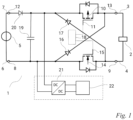
- Fig. 1 shows a circuit arrangement 1 according to a first embodiment of the invention for actuating an electromagnetic linear drive 2.
- the circuit arrangement 1 comprises a ground input 8 for connecting a negative pole 6 of a DC voltage source 5 and a ground output 9 for connecting a first pole 4 of the electromagnetic linear drive 2.
- the circuit arrangement 1 further comprises a supply input 12 for connecting a positive pole 7 of the DC voltage source 5 and a load output 13 for connecting a second pole 3 of the electromagnetic linear drive 2.
- the circuit arrangement 1 further comprises a first, in particular electronically controllable, switching element 10 for selectively disconnecting the load output 13 from and connecting the load output 13 to the supply input 12. To disconnect the load output 13 from the supply input 12, the first switching element 10 must be opened.
- the circuit arrangement 1 also includes a second, in particular electronically controllable, switching element 14 for selectively disconnecting the ground output 9 from and connecting the ground output 9 to the ground input 8. To disconnect the ground output 9 from the ground input 8, the second switching element 14 must be opened.
- Each electronically controllable switching element 10, 14 is designed, for example, as a bipolar transistor, IGBT, a field-effect transistor (FET), a thyristor, or a relay.
- the circuit arrangement 1 includes a control unit 18 for controlling the first switching element 10 and the second switching element 14.
- the control unit 18 is connected to a control input 11 of the first switching element 10 and a control input 15 of the second switching element 14.
- the control unit 18 can be configured to actuate the first switching element 10 and the second switching element 14 synchronously.
- the circuit arrangement comprises a first electronic valve 16, which connects the load output 13 to the ground input 8, and a second electronic valve 17, which connects the ground output 9 to an input side of the first switching element 10.
- the electronic valves 16 and 17 are diodes. However, it can also be provided that the electronic valves are varistors or bidirectional diodes (DIACs).
- the electronic valves 16, 17 each provide electrical connections from the second pole 3 of the electromagnetic linear drive 2 to the ground input 8 and from the first pole 4 of the electromagnetic linear drive 2 to the input side of the first switching element 10. The electrical connections serve to conduct an induced current induced in the electromagnetic linear drive 2 after the electronically controllable switching elements 10, 14 have opened.
- the circuit arrangement 1 advantageously comprises an electrical energy storage device 19 connected to the ground input 8 and the second electronic valve 17, which is charged by the induced induction current.
- the electrical energy storage device 19 and the second electronic valve 17 are preferably connected to the supply input 12.
- the electrical energy storage device 19 can be designed as a capacitor.
- the circuit arrangement 1 advantageously comprises a third electronic valve 20, which connects the supply input 12 to the electrical energy storage device 19.
- the third electronic valve 20 is a diode.
- the circuit arrangement 1 can comprise a DC/DC converter 21 with an input connected to the electrical energy storage device 19 and an output for connecting a further electronic circuit 22.
- the further electronic circuit 22 can also belong to the circuit arrangement 1.
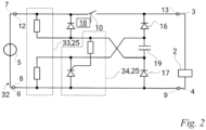
- Fig. 2 shows a circuit arrangement 24 according to a second embodiment of the invention for actuating an electromagnetic linear drive 2.
- the circuit arrangement 24 comprises a ground input 8 for connecting a negative pole 6 of a DC voltage source 5 and a ground output 9 connected to the ground input 8 for connecting a first pole 4 of the electromagnetic linear drive 2.
- the circuit arrangement 24 comprises a supply input 12 for connecting a positive pole 7 of the DC voltage source 5 and a load output 13 for connecting a second pole 3 of the electromagnetic linear drive 2.
- the circuit arrangement 24 also includes a first, in particular electronically controllable, switching element 10 for selectively disconnecting and connecting the load output 13 from the supply input 12. To disconnect the load output 13 from the supply input 12, the first electronically controllable switching element 10 must be opened.
- the first electronically controllable switching element 10 can be a bipolar transistor, IGBT, a field effect transistor (FET), a thyristor, or a relay.
- the circuit arrangement 24 comprises, in contrast to the Fig. 1 shown circuit arrangement 1 does not have a second electronically controllable switching element, ie the ground output 9 is electrically inseparably connected to the ground input 8.
- the circuit arrangement 24 further comprises a control unit 18 for controlling the first switching element 10, which is connected to a control input (not shown) of the first switching element 10.
- the circuit arrangement 24 comprises an electrical energy storage device 19, a first electronic valve 16 connecting the electrical energy storage device 19 to the load output 13, which allows further charging of the electrical energy storage device 19 with an induction current induced in the electromagnetic linear drive 2, and a precharging and discharging circuit 25 for precharging and discharging the electrical energy storage device 19 to a supply voltage provided by the DC voltage source 5.
- the electrical energy storage device 19 can be designed as a capacitor.
- the electrical energy storage device 19 is connected to the electromagnetic linear drive 2 in such a way that, after opening of the first switching element, the induction current induced in the electromagnetic linear drive is conducted to the electrical energy storage device 19 and charges it further, in particular above the level of the supply voltage.
- the pre-charging and discharging circuit 25 ideally comprises at least a second electronic valve 17.
- the second electronic valve 17 connects the ground output 9 to the electrical energy storage device 19 and allows further charging of the electrical energy storage device 19 with the induction current induced in the electromagnetic linear drive 2.
- the pre-charging and discharging circuit 25 can further comprise pre-charging resistors 33, via which the electrical energy storage device 19 can be pre-charged, and a third electronically controllable switching element 34, via which the electrical energy storage device 19 can be discharged to the voltage provided by the DC voltage source 5.
- the third electronically controllable switching element 34 comprises a thyristor. A cathode of the thyristor is connected, on the one hand, via the first electronic valve 16 to the load output 13 and, on the other hand, via a pre-charging resistor 33 to the ground input 8 and the ground output 9. An anode of the thyristor is connected to the ground input 8 and the ground output 9.
- a control input (gate) of the thyristor is connected, via a series resistor that sets a firing voltage of the thyristor, on the one hand, via the second electronic valve 17 to the ground input 8 and the ground output 9 and, on the other hand, via a pre-charging resistor 33 to the supply input 7.
- Fig. 3 shows a circuit arrangement 32 according to a third embodiment of the invention for actuating an electromagnetic linear drive 2.
- the circuit arrangement 32 comprises a ground input 8 for connecting a negative pole 6 of a DC voltage source 5 and a ground output 9 connected to the ground input 8 for connecting a first pole 4 of the electromagnetic linear drive 2.
- the circuit arrangement 32 comprises a supply input 12 for connecting a positive pole 7 of the DC voltage source 5 and a load output 13 for connecting a second pole 3 of the electromagnetic linear drive 2.
- the circuit arrangement 32 also includes a first, in particular electronically controllable, switching element 10 for selectively disconnecting and connecting the load output 13 from the supply input 12. To disconnect the load output 13 from the supply input 12, the first switching element 10 must be opened. To connect a plurality of electromagnetic linear drives 2, the circuit arrangement a corresponding plurality of load outputs 13, electronically controllable first switching elements 10 and first electronic valves 16.
- the circuit arrangement 32 further comprises a control unit 18 for controlling the first switching element 10, which is connected to a control input (not shown) of the first switching element 10.
- the circuit arrangement 24 comprises an electrical energy storage device 19, a first electronic valve 16 connecting the electrical energy storage device 19 to the load output 13, which allows further charging of the electrical energy storage device 19 with an induction current induced in the electromagnetic linear drive 2, and a precharging and discharging circuit 25 for precharging and discharging the electrical energy storage device 19 to a supply voltage provided by the DC voltage source 5.
- the electrical energy storage device 19 can be designed as a capacitor.
- the pre-discharge and discharge circuit 25 may comprise a bidirectional charge pump that provides the electrical energy storage 19.
- the electrical energy storage 19 is connected to the ground input 8, the ground output 9, and the first electronic valve 16 connected to the load output 13.
- the electrical energy storage device 19 is connected to the electromagnetic linear drive 2 in such a way that, after the first switching element 10 is opened, the induction current induced in the electromagnetic linear drive 2 is conducted to the electrical energy storage device 19 and further charges it.
- the bidirectional charge pump can comprise a further electrical energy storage device 26 for charging and discharging the electrical energy storage device 19.
- the further electrical energy storage device 26 can be designed as a capacitor.
- the bidirectional charge pump advantageously comprises at least one third electronically controllable switching element, here four electronically controllable switching elements 27, 28, 29, 30, each with a control input (not shown) connected to the control unit 18, via which the electrical energy storage device 19 can be precharged, in particular, to the supply voltage provided by the DC voltage source 5, or discharged to the voltage provided by the DC voltage source 5.
- Each electronically controllable switching element 10, 14, 27, 28, 29, 30 is designed, for example, as a bipolar transistor, IGBT, a field-effect transistor (FET), a thyristor, or a relay.
- the pre-discharge and discharge circuit 25 can comprise at least one coil 31.
- the coil 31 serves to minimize energy losses.
- the coil 31 allows energy to be temporarily stored in the magnetic field of the coil 31 and then passed on to the energy storage device 19 and/or to the additional energy storage device 26. This can prevent energy from being lost in the form of heat.
- the coil 31 is electrically arranged between the DC voltage source 5 and the energy storage device 19.
- the coil 31 is electrically arranged between the energy storage device 19 and the additional energy storage device 26.
- the further electrical energy storage device 26 is electrically connected to the positive pole 7, in particular to the supply input 12, via the first further electronically controllable switching element 27.
- the negative pole 6, in particular the ground input 8 is electrically connected to the further energy storage device 26 via the second further electronically controllable switching element 28.
- the third further electronically controllable switching element 29 is electrically arranged between the electrical energy storage device 19 and the further electrical energy storage device 26, in particular the coil 31.
- the fourth further electronically controllable switching element 30 connects the electrical connection between the electrical energy store 19 and the further electrical energy store 26, in particular between the further electrical energy store 26 and the coil 31, electrically connected to the negative pole 6, in particular to the ground output 8.
- the further electrical energy store 26 is electrically arranged between the electrical energy store 19 and the negative pole 6, in particular to the ground input 8.
- the electrical energy store 19 and the further electrical energy store 26 are electrically connectable via the second further electronically controllable switching element 28.
- the first further electronically controllable switching element 27 is bridged by an electronic valve which, in the conventional current direction, allows current to flow from the further electrical energy storage device 26 to the positive pole 7, in particular to the supply input 12, and blocks it in the opposite direction.
- the second further electronically controllable switching element 28 is bridged by an electronic valve which, in the conventional current direction, allows current to flow from the electrical energy storage device 19 to the further electrical energy storage device 26 and blocks it in the opposite direction.
- the third further electronically controllable switching element 29 is bridged by an electronic valve which, in the conventional current direction, allows current to flow from the electrical energy storage device 19 to the further electrical energy storage device 26 and blocks it in the opposite direction.
- the fourth further electronically controllable switching element 30 is bridged by an electronic valve which allows current flow from the further electrical energy storage device 26 to the negative pole 6, in particular to the ground input 8, in the conventional current direction and blocks it in the opposite direction.
- the additional electrical energy storage device 26 is first charged.
- the first additional electronically controllable switching element is closed so that charge can flow through and the additional electrical energy storage device 26 can be charged.
- the fourth additional electronically controllable switching element 30 is open and is connected to the associated electronic valve is bridged.
- One side of the further electrical energy store 26, which in the exemplary embodiment is designed as a capacitor is then electrically connected to the positive pole 7, in particular to the supply input 12, via the first further electronically controllable switching element 27.
- the other side of the further electrical energy store 26, which in the exemplary embodiment is designed as a capacitor is then electrically connected to the negative pole 6, in particular to the ground input 8, via the electronic valve assigned to the fourth further electronically controllable switching element 30.
- the second further electronically controllable switching element 28 and the third further electronically controllable switching element 29 are open in this first charging step of the pre-discharging and discharging circuit 25.
- the first additional electronically controllable switching element 27 is opened.
- the additional energy storage device 26 which is charged in particular to the supply voltage, is electrically connected to the negative pole 6, in particular to the ground input 8, by which the switching element is closed.
- the electrical energy storage device 19 is charged.
- the electrical energy storage device 19 is connected to the additional electrical energy storage device 26 via the electronic valve assigned to the third additional electronically controllable switching element 29.
- the third additional electronically controllable switching element 29 is open.
- the electrical energy storage device 19 is charged to a negative potential.
- the two charging steps can be repeated several times, so that the negative potential of the electrical energy storage device 19 can be greater in magnitude than the supply voltage. This process of charging the electrical energy storage device 19 is also referred to as charge pumping.
- the first further electronically controllable switching element 27, the second further electronically controllable switching element 28 and the fourth further electronically controllable switching element 30 are opened.
- the third further electronically controllable switching element 29 is closed.
- the second further electronically controllable switching element 28 is bridged by the associated electronic valve, so that in the first discharge step, regardless of the position of the second further electronically controllable switching element 28, current can flow in the conventional current direction from the further electrical energy store 26 to the electrical energy store 19.
- the further electrical energy store 26 is charged. If the voltage of the first electrical energy store 19 is higher or was higher before the first discharge step, the further energy store 26 is thereby charged to a voltage that is higher than the supply voltage.
- the additional electrical energy storage device 26 can be discharged toward the supply voltage.
- the fourth additional electronically controllable switching element 30 is closed. All other switching elements 27, 28, and 29 are open. The current flows in the conventional current direction through the electronic valve associated with the first additional electronically controllable switching element 27.
- the electrical energy storage device 19 can be charged and discharged by the pre-charging and discharging circuit 25.
- the electrical energy storage device 19 pre-charged by the pre-charging and discharging circuit 25 can be further charged with an induction current induced in the electromagnetic linear drive 2.
- each circuit arrangement according to the invention in particular each circuit arrangement 1, 14, 32 described above, can comprise the DC voltage source 5 connected to the supply input 12 and the ground input 8, into which the induced induction current is fed.
- an inventive Circuit arrangement 1, 14, 32 belongs to an electromagnetic linear drive 2 or to a connector for controlling a solenoid valve, wherein the connector comprises, in addition to the circuit arrangement 1, 14, 32, an electromagnetic linear drive 2 connected to the circuit arrangement on the output side.
- the circuit arrangement 1, 14, 32 can be arranged in a housing of the connector or the solenoid valve.
Landscapes
- Physics & Mathematics (AREA)
- Electromagnetism (AREA)
- Engineering & Computer Science (AREA)
- Power Engineering (AREA)
- Electronic Switches (AREA)
- Magnetically Actuated Valves (AREA)
Priority Applications (2)
| Application Number | Priority Date | Filing Date | Title |
|---|---|---|---|
| EP23214312.3A EP4567842A1 (fr) | 2023-12-05 | 2023-12-05 | Circuit pour actionner un actionneur lineaire electromagnetique |
| US18/967,874 US20250182943A1 (en) | 2023-12-05 | 2024-12-04 | Electronic circuit for actuating an electromagnetic linear actuator |
Applications Claiming Priority (1)
| Application Number | Priority Date | Filing Date | Title |
|---|---|---|---|
| EP23214312.3A EP4567842A1 (fr) | 2023-12-05 | 2023-12-05 | Circuit pour actionner un actionneur lineaire electromagnetique |
Publications (1)
| Publication Number | Publication Date |
|---|---|
| EP4567842A1 true EP4567842A1 (fr) | 2025-06-11 |
Family
ID=89119239
Family Applications (1)
| Application Number | Title | Priority Date | Filing Date |
|---|---|---|---|
| EP23214312.3A Pending EP4567842A1 (fr) | 2023-12-05 | 2023-12-05 | Circuit pour actionner un actionneur lineaire electromagnetique |
Country Status (2)
| Country | Link |
|---|---|
| US (1) | US20250182943A1 (fr) |
| EP (1) | EP4567842A1 (fr) |
Citations (6)
| Publication number | Priority date | Publication date | Assignee | Title |
|---|---|---|---|---|
| EP1067668A2 (fr) * | 1999-07-09 | 2001-01-10 | WABCO GmbH & CO. OHG | Circuit pour commander un actionneur électromagnétique |
| EP1065677B1 (fr) * | 1999-06-30 | 2004-10-20 | Denso Corporation | Dispositif de contrôle d'une charge électromagnétique avec alimentation d'entraínement et de démarrage variable |
| US20070188967A1 (en) * | 2006-02-10 | 2007-08-16 | Eaton Corporation | Solenoid driver circuit |
| DE102012207947A1 (de) * | 2011-05-23 | 2012-11-29 | Denso Corporation | Magnetventilansteuervorrichtung |
| DE102017008944A1 (de) * | 2017-09-23 | 2019-03-28 | Hydac Accessories Gmbh | Adaptervorrichtung nebst Verfahren zur Regelung eines Steuerstromes |
| EP3822993A1 (fr) * | 2019-11-13 | 2021-05-19 | Minimax Viking Research & Development GmbH | Procédé et dispositif de commande électrique d'un actionneur |
-
2023
- 2023-12-05 EP EP23214312.3A patent/EP4567842A1/fr active Pending
-
2024
- 2024-12-04 US US18/967,874 patent/US20250182943A1/en active Pending
Patent Citations (6)
| Publication number | Priority date | Publication date | Assignee | Title |
|---|---|---|---|---|
| EP1065677B1 (fr) * | 1999-06-30 | 2004-10-20 | Denso Corporation | Dispositif de contrôle d'une charge électromagnétique avec alimentation d'entraínement et de démarrage variable |
| EP1067668A2 (fr) * | 1999-07-09 | 2001-01-10 | WABCO GmbH & CO. OHG | Circuit pour commander un actionneur électromagnétique |
| US20070188967A1 (en) * | 2006-02-10 | 2007-08-16 | Eaton Corporation | Solenoid driver circuit |
| DE102012207947A1 (de) * | 2011-05-23 | 2012-11-29 | Denso Corporation | Magnetventilansteuervorrichtung |
| DE102017008944A1 (de) * | 2017-09-23 | 2019-03-28 | Hydac Accessories Gmbh | Adaptervorrichtung nebst Verfahren zur Regelung eines Steuerstromes |
| EP3822993A1 (fr) * | 2019-11-13 | 2021-05-19 | Minimax Viking Research & Development GmbH | Procédé et dispositif de commande électrique d'un actionneur |
Also Published As
| Publication number | Publication date |
|---|---|
| US20250182943A1 (en) | 2025-06-05 |
Similar Documents
| Publication | Publication Date | Title |
|---|---|---|
| DE2058091C3 (de) | Steuerschaltung für die Impulssteuerung eines Gleichstrommotors | |
| DE102004005770B4 (de) | Schaltung zur Steuerung mehrerer Magnetantriebe und Leistungsschaltvorrichtung mit einer derartigen Schaltung | |
| EP1527470B1 (fr) | Ensemble de commande pour entrainement electromagnetique | |
| DE102011004733A1 (de) | Submodul eines modularen Mehrstufenumrichters | |
| DE3702680A1 (de) | Verfahren und schaltung zur ansteuerung von elektromagnetischen verbrauchern | |
| EP3853957B1 (fr) | Commutateur électronique à protection contre les surtensions | |
| DE19723935C1 (de) | Vorrichtung und Verfahren zum Ansteuern wenigstens eines kapazitiven Stellgliedes | |
| EP3915127B1 (fr) | Disjoncteur à courant continu | |
| DE102012017679A1 (de) | Vorladeeinrichtung und Verfahren zum Koppeln einer HV-Batterie mit einem Fahrzeugnetz | |
| DE10341582B4 (de) | Schaltungsanordnung zum schnellen Schalten induktiver Lasten | |
| EP0601352B1 (fr) | Dispositif de freinage pour un moteur série à collecteur | |
| EP4567842A1 (fr) | Circuit pour actionner un actionneur lineaire electromagnetique | |
| EP0418545A2 (fr) | Circuit électrique de dÀ©gagement au blocage d'un commutateur semi-conducteur commandable | |
| DE19632365C1 (de) | Schaltungsanordnung zum voneinander unabhängigen Schalten mehrerer, paralleler induktiver Schalteinheiten | |
| DE102011016056A1 (de) | Hybrides Schaltelement, Schaltungsanordnung und Verfahren zur Steuerung eines hybriden Schaltelements einer Schaltungsanordnung | |
| DE4229440B4 (de) | Schaltungsanordnung zum Ein- und Ausschalten einer elektrischen Last | |
| DE69028916T2 (de) | Vorrichtung zur dämpfung des rücklaufstromes | |
| WO2018073029A1 (fr) | Ensemble circuit destiné à la précharge d'un condensateur de circuit intermédiaire d'un réseau de bord haute tension | |
| EP1203389B1 (fr) | Montage pour un appareil de commutation electromagnetique | |
| DE102009006618A1 (de) | Schaltungsanordnung zum Betreiben eines elektrischen Verbrauchers und Verfahren zum Schalten eines Halbleiterschalters, insbesondere eines MOSFETs | |
| DE102010001622A1 (de) | Verfahren zum Entregen bei einer elektrischen Maschine | |
| DE1288194B (de) | Schaltungsanordnung zur Schnellerregung von gleichstrombetriebenen Elektromagneten | |
| DE102014212263A1 (de) | Schaltungsanordnung zur selbstregelnden Anlaufstrombegrenzung einer elektrischen Maschine | |
| DE102020215711B4 (de) | Auslösevorrichtung für einen Leistungsschalter | |
| WO2020052947A1 (fr) | Module relais |
Legal Events
| Date | Code | Title | Description |
|---|---|---|---|
| PUAI | Public reference made under article 153(3) epc to a published international application that has entered the european phase |
Free format text: ORIGINAL CODE: 0009012 |
|
| STAA | Information on the status of an ep patent application or granted ep patent |
Free format text: STATUS: THE APPLICATION HAS BEEN PUBLISHED |
|
| AK | Designated contracting states |
Kind code of ref document: A1 Designated state(s): AL AT BE BG CH CY CZ DE DK EE ES FI FR GB GR HR HU IE IS IT LI LT LU LV MC ME MK MT NL NO PL PT RO RS SE SI SK SM TR |
|
| STAA | Information on the status of an ep patent application or granted ep patent |
Free format text: STATUS: REQUEST FOR EXAMINATION WAS MADE |
|
| 17P | Request for examination filed |
Effective date: 20251211 |