EP4567887A2 - Liaison hybride utilisant des contacts de liaison factices et des interconnexions factices - Google Patents
Liaison hybride utilisant des contacts de liaison factices et des interconnexions factices Download PDFInfo
- Publication number
- EP4567887A2 EP4567887A2 EP25170040.7A EP25170040A EP4567887A2 EP 4567887 A2 EP4567887 A2 EP 4567887A2 EP 25170040 A EP25170040 A EP 25170040A EP 4567887 A2 EP4567887 A2 EP 4567887A2
- Authority
- EP
- European Patent Office
- Prior art keywords
- bonding
- layer
- contacts
- interconnect
- interconnects
- Prior art date
- Legal status (The legal status is an assumption and is not a legal conclusion. Google has not performed a legal analysis and makes no representation as to the accuracy of the status listed.)
- Pending
Links
Images


Classifications
-
- H—ELECTRICITY
- H10—SEMICONDUCTOR DEVICES; ELECTRIC SOLID-STATE DEVICES NOT OTHERWISE PROVIDED FOR
- H10B—ELECTRONIC MEMORY DEVICES
- H10B41/00—Electrically erasable-and-programmable ROM [EEPROM] devices comprising floating gates
- H10B41/50—Electrically erasable-and-programmable ROM [EEPROM] devices comprising floating gates characterised by the boundary region between the core region and the peripheral circuit region
-
- H—ELECTRICITY
- H10—SEMICONDUCTOR DEVICES; ELECTRIC SOLID-STATE DEVICES NOT OTHERWISE PROVIDED FOR
- H10W—GENERIC PACKAGES, INTERCONNECTIONS, CONNECTORS OR OTHER CONSTRUCTIONAL DETAILS OF DEVICES COVERED BY CLASS H10
- H10W20/00—Interconnections in chips, wafers or substrates
- H10W20/40—Interconnections external to wafers or substrates, e.g. back-end-of-line [BEOL] metallisations or vias connecting to gate electrodes
- H10W20/41—Interconnections external to wafers or substrates, e.g. back-end-of-line [BEOL] metallisations or vias connecting to gate electrodes characterised by their conductive parts
- H10W20/425—Barrier, adhesion or liner layers
-
- H—ELECTRICITY
- H10—SEMICONDUCTOR DEVICES; ELECTRIC SOLID-STATE DEVICES NOT OTHERWISE PROVIDED FOR
- H10B—ELECTRONIC MEMORY DEVICES
- H10B41/00—Electrically erasable-and-programmable ROM [EEPROM] devices comprising floating gates
- H10B41/20—Electrically erasable-and-programmable ROM [EEPROM] devices comprising floating gates characterised by three-dimensional [3D] arrangements, e.g. with cells on different height levels
- H10B41/23—Electrically erasable-and-programmable ROM [EEPROM] devices comprising floating gates characterised by three-dimensional [3D] arrangements, e.g. with cells on different height levels with source and drain on different levels, e.g. with sloping channels
- H10B41/27—Electrically erasable-and-programmable ROM [EEPROM] devices comprising floating gates characterised by three-dimensional [3D] arrangements, e.g. with cells on different height levels with source and drain on different levels, e.g. with sloping channels the channels comprising vertical portions, e.g. U-shaped channels
-
- H—ELECTRICITY
- H10—SEMICONDUCTOR DEVICES; ELECTRIC SOLID-STATE DEVICES NOT OTHERWISE PROVIDED FOR
- H10B—ELECTRONIC MEMORY DEVICES
- H10B43/00—EEPROM devices comprising charge-trapping gate insulators
- H10B43/20—EEPROM devices comprising charge-trapping gate insulators characterised by three-dimensional [3D] arrangements, e.g. with cells on different height levels
- H10B43/23—EEPROM devices comprising charge-trapping gate insulators characterised by three-dimensional [3D] arrangements, e.g. with cells on different height levels with source and drain on different levels, e.g. with sloping channels
- H10B43/27—EEPROM devices comprising charge-trapping gate insulators characterised by three-dimensional [3D] arrangements, e.g. with cells on different height levels with source and drain on different levels, e.g. with sloping channels the channels comprising vertical portions, e.g. U-shaped channels
-
- H—ELECTRICITY
- H10—SEMICONDUCTOR DEVICES; ELECTRIC SOLID-STATE DEVICES NOT OTHERWISE PROVIDED FOR
- H10B—ELECTRONIC MEMORY DEVICES
- H10B43/00—EEPROM devices comprising charge-trapping gate insulators
- H10B43/30—EEPROM devices comprising charge-trapping gate insulators characterised by the memory core region
- H10B43/35—EEPROM devices comprising charge-trapping gate insulators characterised by the memory core region with cell select transistors, e.g. NAND
-
- H—ELECTRICITY
- H10—SEMICONDUCTOR DEVICES; ELECTRIC SOLID-STATE DEVICES NOT OTHERWISE PROVIDED FOR
- H10B—ELECTRONIC MEMORY DEVICES
- H10B43/00—EEPROM devices comprising charge-trapping gate insulators
- H10B43/50—EEPROM devices comprising charge-trapping gate insulators characterised by the boundary region between the core and peripheral circuit regions
-
- H—ELECTRICITY
- H10—SEMICONDUCTOR DEVICES; ELECTRIC SOLID-STATE DEVICES NOT OTHERWISE PROVIDED FOR
- H10W—GENERIC PACKAGES, INTERCONNECTIONS, CONNECTORS OR OTHER CONSTRUCTIONAL DETAILS OF DEVICES COVERED BY CLASS H10
- H10W20/00—Interconnections in chips, wafers or substrates
- H10W20/01—Manufacture or treatment
- H10W20/031—Manufacture or treatment of conductive parts of the interconnections
- H10W20/032—Manufacture or treatment of conductive parts of the interconnections of conductive barrier, adhesion or liner layers
-
- H—ELECTRICITY
- H10—SEMICONDUCTOR DEVICES; ELECTRIC SOLID-STATE DEVICES NOT OTHERWISE PROVIDED FOR
- H10W—GENERIC PACKAGES, INTERCONNECTIONS, CONNECTORS OR OTHER CONSTRUCTIONAL DETAILS OF DEVICES COVERED BY CLASS H10
- H10W70/00—Package substrates; Interposers; Redistribution layers [RDL]
- H10W70/01—Manufacture or treatment
- H10W70/05—Manufacture or treatment of insulating or insulated package substrates, or of interposers, or of redistribution layers
- H10W70/08—Manufacture or treatment of insulating or insulated package substrates, or of interposers, or of redistribution layers by depositing layers on the chip or wafer, e.g. "chip-first" RDLs
- H10W70/09—Manufacture or treatment of insulating or insulated package substrates, or of interposers, or of redistribution layers by depositing layers on the chip or wafer, e.g. "chip-first" RDLs extending onto an encapsulation that laterally surrounds the chip or wafer, e.g. fan-out wafer level package [FOWLP] RDLs
-
- H—ELECTRICITY
- H10—SEMICONDUCTOR DEVICES; ELECTRIC SOLID-STATE DEVICES NOT OTHERWISE PROVIDED FOR
- H10W—GENERIC PACKAGES, INTERCONNECTIONS, CONNECTORS OR OTHER CONSTRUCTIONAL DETAILS OF DEVICES COVERED BY CLASS H10
- H10W70/00—Package substrates; Interposers; Redistribution layers [RDL]
- H10W70/60—Insulating or insulated package substrates; Interposers; Redistribution layers
- H10W70/611—Insulating or insulated package substrates; Interposers; Redistribution layers for connecting multiple chips together
-
- H—ELECTRICITY
- H10—SEMICONDUCTOR DEVICES; ELECTRIC SOLID-STATE DEVICES NOT OTHERWISE PROVIDED FOR
- H10W—GENERIC PACKAGES, INTERCONNECTIONS, CONNECTORS OR OTHER CONSTRUCTIONAL DETAILS OF DEVICES COVERED BY CLASS H10
- H10W70/00—Package substrates; Interposers; Redistribution layers [RDL]
- H10W70/60—Insulating or insulated package substrates; Interposers; Redistribution layers
- H10W70/62—Insulating or insulated package substrates; Interposers; Redistribution layers characterised by their interconnections
- H10W70/63—Vias, e.g. via plugs
- H10W70/635—Through-vias
-
- H—ELECTRICITY
- H10—SEMICONDUCTOR DEVICES; ELECTRIC SOLID-STATE DEVICES NOT OTHERWISE PROVIDED FOR
- H10W—GENERIC PACKAGES, INTERCONNECTIONS, CONNECTORS OR OTHER CONSTRUCTIONAL DETAILS OF DEVICES COVERED BY CLASS H10
- H10W72/00—Interconnections or connectors in packages
- H10W72/01—Manufacture or treatment
- H10W72/019—Manufacture or treatment of bond pads
-
- H—ELECTRICITY
- H10—SEMICONDUCTOR DEVICES; ELECTRIC SOLID-STATE DEVICES NOT OTHERWISE PROVIDED FOR
- H10W—GENERIC PACKAGES, INTERCONNECTIONS, CONNECTORS OR OTHER CONSTRUCTIONAL DETAILS OF DEVICES COVERED BY CLASS H10
- H10W72/00—Interconnections or connectors in packages
- H10W72/90—Bond pads, in general
-
- H—ELECTRICITY
- H10—SEMICONDUCTOR DEVICES; ELECTRIC SOLID-STATE DEVICES NOT OTHERWISE PROVIDED FOR
- H10W—GENERIC PACKAGES, INTERCONNECTIONS, CONNECTORS OR OTHER CONSTRUCTIONAL DETAILS OF DEVICES COVERED BY CLASS H10
- H10W80/00—Direct bonding of chips, wafers or substrates
-
- H—ELECTRICITY
- H10—SEMICONDUCTOR DEVICES; ELECTRIC SOLID-STATE DEVICES NOT OTHERWISE PROVIDED FOR
- H10W—GENERIC PACKAGES, INTERCONNECTIONS, CONNECTORS OR OTHER CONSTRUCTIONAL DETAILS OF DEVICES COVERED BY CLASS H10
- H10W90/00—Package configurations
-
- H—ELECTRICITY
- H10—SEMICONDUCTOR DEVICES; ELECTRIC SOLID-STATE DEVICES NOT OTHERWISE PROVIDED FOR
- H10W—GENERIC PACKAGES, INTERCONNECTIONS, CONNECTORS OR OTHER CONSTRUCTIONAL DETAILS OF DEVICES COVERED BY CLASS H10
- H10W70/00—Package substrates; Interposers; Redistribution layers [RDL]
- H10W70/01—Manufacture or treatment
- H10W70/05—Manufacture or treatment of insulating or insulated package substrates, or of interposers, or of redistribution layers
- H10W70/093—Connecting or disconnecting other interconnections thereto or therefrom, e.g. connecting bond wires or bumps
-
- H—ELECTRICITY
- H10—SEMICONDUCTOR DEVICES; ELECTRIC SOLID-STATE DEVICES NOT OTHERWISE PROVIDED FOR
- H10W—GENERIC PACKAGES, INTERCONNECTIONS, CONNECTORS OR OTHER CONSTRUCTIONAL DETAILS OF DEVICES COVERED BY CLASS H10
- H10W72/00—Interconnections or connectors in packages
- H10W72/01—Manufacture or treatment
- H10W72/019—Manufacture or treatment of bond pads
- H10W72/01931—Manufacture or treatment of bond pads using blanket deposition
- H10W72/01938—Manufacture or treatment of bond pads using blanket deposition in gaseous form, e.g. by CVD or PVD
-
- H—ELECTRICITY
- H10—SEMICONDUCTOR DEVICES; ELECTRIC SOLID-STATE DEVICES NOT OTHERWISE PROVIDED FOR
- H10W—GENERIC PACKAGES, INTERCONNECTIONS, CONNECTORS OR OTHER CONSTRUCTIONAL DETAILS OF DEVICES COVERED BY CLASS H10
- H10W72/00—Interconnections or connectors in packages
- H10W72/01—Manufacture or treatment
- H10W72/019—Manufacture or treatment of bond pads
- H10W72/01951—Changing the shapes of bond pads
- H10W72/01953—Changing the shapes of bond pads by etching
-
- H—ELECTRICITY
- H10—SEMICONDUCTOR DEVICES; ELECTRIC SOLID-STATE DEVICES NOT OTHERWISE PROVIDED FOR
- H10W—GENERIC PACKAGES, INTERCONNECTIONS, CONNECTORS OR OTHER CONSTRUCTIONAL DETAILS OF DEVICES COVERED BY CLASS H10
- H10W72/00—Interconnections or connectors in packages
- H10W72/90—Bond pads, in general
- H10W72/931—Shapes of bond pads
- H10W72/934—Cross-sectional shape, i.e. in side view
-
- H—ELECTRICITY
- H10—SEMICONDUCTOR DEVICES; ELECTRIC SOLID-STATE DEVICES NOT OTHERWISE PROVIDED FOR
- H10W—GENERIC PACKAGES, INTERCONNECTIONS, CONNECTORS OR OTHER CONSTRUCTIONAL DETAILS OF DEVICES COVERED BY CLASS H10
- H10W72/00—Interconnections or connectors in packages
- H10W72/90—Bond pads, in general
- H10W72/941—Dispositions of bond pads
-
- H—ELECTRICITY
- H10—SEMICONDUCTOR DEVICES; ELECTRIC SOLID-STATE DEVICES NOT OTHERWISE PROVIDED FOR
- H10W—GENERIC PACKAGES, INTERCONNECTIONS, CONNECTORS OR OTHER CONSTRUCTIONAL DETAILS OF DEVICES COVERED BY CLASS H10
- H10W72/00—Interconnections or connectors in packages
- H10W72/90—Bond pads, in general
- H10W72/951—Materials of bond pads
- H10W72/952—Materials of bond pads comprising metals or metalloids, e.g. PbSn, Ag or Cu
-
- H—ELECTRICITY
- H10—SEMICONDUCTOR DEVICES; ELECTRIC SOLID-STATE DEVICES NOT OTHERWISE PROVIDED FOR
- H10W—GENERIC PACKAGES, INTERCONNECTIONS, CONNECTORS OR OTHER CONSTRUCTIONAL DETAILS OF DEVICES COVERED BY CLASS H10
- H10W72/00—Interconnections or connectors in packages
- H10W72/90—Bond pads, in general
- H10W72/961—Functions of bonds pads
- H10W72/963—Providing mechanical bonding or support, e.g. dummy bond pads
-
- H—ELECTRICITY
- H10—SEMICONDUCTOR DEVICES; ELECTRIC SOLID-STATE DEVICES NOT OTHERWISE PROVIDED FOR
- H10W—GENERIC PACKAGES, INTERCONNECTIONS, CONNECTORS OR OTHER CONSTRUCTIONAL DETAILS OF DEVICES COVERED BY CLASS H10
- H10W72/00—Interconnections or connectors in packages
- H10W72/90—Bond pads, in general
- H10W72/961—Functions of bonds pads
- H10W72/967—Multiple bond pads having different functions
-
- H—ELECTRICITY
- H10—SEMICONDUCTOR DEVICES; ELECTRIC SOLID-STATE DEVICES NOT OTHERWISE PROVIDED FOR
- H10W—GENERIC PACKAGES, INTERCONNECTIONS, CONNECTORS OR OTHER CONSTRUCTIONAL DETAILS OF DEVICES COVERED BY CLASS H10
- H10W80/00—Direct bonding of chips, wafers or substrates
- H10W80/011—Manufacture or treatment of pads or other interconnections to be direct bonded
- H10W80/016—Cleaning
-
- H—ELECTRICITY
- H10—SEMICONDUCTOR DEVICES; ELECTRIC SOLID-STATE DEVICES NOT OTHERWISE PROVIDED FOR
- H10W—GENERIC PACKAGES, INTERCONNECTIONS, CONNECTORS OR OTHER CONSTRUCTIONAL DETAILS OF DEVICES COVERED BY CLASS H10
- H10W80/00—Direct bonding of chips, wafers or substrates
- H10W80/011—Manufacture or treatment of pads or other interconnections to be direct bonded
- H10W80/041—Thermally treating
-
- H—ELECTRICITY
- H10—SEMICONDUCTOR DEVICES; ELECTRIC SOLID-STATE DEVICES NOT OTHERWISE PROVIDED FOR
- H10W—GENERIC PACKAGES, INTERCONNECTIONS, CONNECTORS OR OTHER CONSTRUCTIONAL DETAILS OF DEVICES COVERED BY CLASS H10
- H10W80/00—Direct bonding of chips, wafers or substrates
- H10W80/301—Bonding techniques, e.g. hybrid bonding
- H10W80/312—Bonding techniques, e.g. hybrid bonding characterised by the direct bonding of electrically conductive pads
-
- H—ELECTRICITY
- H10—SEMICONDUCTOR DEVICES; ELECTRIC SOLID-STATE DEVICES NOT OTHERWISE PROVIDED FOR
- H10W—GENERIC PACKAGES, INTERCONNECTIONS, CONNECTORS OR OTHER CONSTRUCTIONAL DETAILS OF DEVICES COVERED BY CLASS H10
- H10W80/00—Direct bonding of chips, wafers or substrates
- H10W80/301—Bonding techniques, e.g. hybrid bonding
- H10W80/327—Bonding techniques, e.g. hybrid bonding characterised by the direct bonding of insulating parts, e.g. of silicon oxide layers
-
- H—ELECTRICITY
- H10—SEMICONDUCTOR DEVICES; ELECTRIC SOLID-STATE DEVICES NOT OTHERWISE PROVIDED FOR
- H10W—GENERIC PACKAGES, INTERCONNECTIONS, CONNECTORS OR OTHER CONSTRUCTIONAL DETAILS OF DEVICES COVERED BY CLASS H10
- H10W80/00—Direct bonding of chips, wafers or substrates
- H10W80/701—Direct bonding of chips, wafers or substrates characterised by the pads after the direct bonding
- H10W80/732—Direct bonding of chips, wafers or substrates characterised by the pads after the direct bonding having shape changed during the connecting
-
- H—ELECTRICITY
- H10—SEMICONDUCTOR DEVICES; ELECTRIC SOLID-STATE DEVICES NOT OTHERWISE PROVIDED FOR
- H10W—GENERIC PACKAGES, INTERCONNECTIONS, CONNECTORS OR OTHER CONSTRUCTIONAL DETAILS OF DEVICES COVERED BY CLASS H10
- H10W90/00—Package configurations
- H10W90/701—Package configurations characterised by the relative positions of pads or connectors relative to package parts
- H10W90/791—Package configurations characterised by the relative positions of pads or connectors relative to package parts of direct-bonded pads
- H10W90/792—Package configurations characterised by the relative positions of pads or connectors relative to package parts of direct-bonded pads between multiple chips
Definitions
- Embodiments of the present disclosure relate to bonded semiconductor structures and fabrication methods thereof.
- Planar semiconductor devices such as memory cells
- Planar semiconductor devices are scaled to smaller sizes by improving process technology, circuit design, programming algorithm, and fabrication process.
- process technology circuit design, programming algorithm, and fabrication process.
- feature sizes of the semiconductor devices approach a lower limit
- planar process and fabrication techniques become challenging and costly.
- a three-dimensional (3D) device architecture can address the density limitation in some planar semiconductor devices, for example, Flash memory devices.
- a 3D semiconductor device can be formed by stacking semiconductor wafers or dies and interconnecting them vertically using, for instance, through-silicon vias (TSVs) or copper-to-copper (Cu-Cu) connections, so that the resulting structure acts as a single device to achieve performance improvements at reduced power and smaller footprint than conventional planar processes.
- TSVs through-silicon vias
- Cu-Cu copper-to-copper
- Embodiments of semiconductor devices, bonded structures, and fabrication methods thereof are disclosed herein.
- a semiconductor device in one example, includes a first semiconductor structure and a second semiconductor structure.
- the first semiconductor structure includes a first interconnect layer including a plurality of first interconnects. At least one of the first interconnects is at least one first dummy interconnect.
- the first semiconductor structure further includes a first bonding layer including a plurality of first bonding contacts. Each of the first interconnects is in contact with a respective one of the first bonding contacts.
- the second semiconductor structure includes a second interconnect layer including a plurality of second interconnects. At least one of the second interconnects is at least one second dummy interconnect.
- the second semiconductor structure further includes a second bonding layer including a plurality of second bonding contacts.
- the semiconductor device further includes a bonding interface between the first bonding layer and the second bonding layer.
- Each of the first bonding contacts is in contact with a respective one of the second bonding contacts at the bonding interface.
- a bonded structure in another example, includes a bonding interface, a pair of functional bonding contacts, and a pair of dummy bonding contacts.
- the pair of functional bonding contacts are in contact with one another at the bonding interface.
- the pair of bonding contacts are in contact with a pair of functional interconnects on opposite sides of the bonding interface, respectively.
- the pair of dummy bonding contacts are in contact with one another at the bonding interface.
- the pair of dummy bonding contacts are in contact with a pair of dummy interconnects on the opposite sides of the bonding interface, respectively.
- a method for forming a semiconductor device is disclosed.
- a first interconnect layer including a plurality of first interconnects is formed above a first substrate. At least one of the first interconnects is at least one first dummy interconnect.
- a first bonding layer including a plurality of first bonding contacts is formed above the first interconnect layer, such that each of the first interconnects is in contact with a respective one of the first bonding contacts.
- a second interconnect layer including a plurality of second interconnects is formed above a second substrate. At least one of the second interconnects is at least one second dummy interconnect.
- a second bonding layer including a plurality of second bonding contacts is formed above the second interconnect layer, such that each of the second interconnects is in contact with a respective one of the second bonding contacts.
- the first substrate and the second substrate are bonded in a face-to-face manner, such that each of the first bonding contacts is in contact with a respective one of the second bonding contacts at a bonding interface.
- references in the specification to "one embodiment,” “an embodiment,” “an example embodiment,” “some embodiments,” etc. indicate that the embodiment described may include a particular feature, structure, or characteristic, but every embodiment may not necessarily include the particular feature, structure, or characteristic. Moreover, such phrases do not necessarily refer to the same embodiment. Further, when a particular feature, structure or characteristic is described in connection with an embodiment, it would be within the knowledge of a person skilled in the pertinent art to effect such feature, structure or characteristic in connection with other embodiments whether or not explicitly described.
- terminology may be understood at least in part from usage in context.
- the term “one or more” as used herein, depending at least in part upon context may be used to describe any feature, structure, or characteristic in a singular sense or may be used to describe combinations of features, structures or characteristics in a plural sense.
- terms, such as “a,” “an,” or “the,” again, may be understood to convey a singular usage or to convey a plural usage, depending at least in part upon context.
- the term “based on” may be understood as not necessarily intended to convey an exclusive set of factors and may, instead, allow for existence of additional factors not necessarily expressly described, again, depending at least in part on context.
- spatially relative terms such as “beneath,” “below,” “lower,” “above,” “upper,” and the like, may be used herein for ease of description to describe one element or feature's relationship to another element(s) or feature(s) as illustrated in the figures.
- the spatially relative terms are intended to encompass different orientations of the device in use or operation in addition to the orientation depicted in the figures.
- the apparatus may be otherwise oriented (rotated 90 degrees or at other orientations) and the spatially relative descriptors used herein may likewise be interpreted accordingly.
- the term "substrate” refers to a material onto which subsequent material layers are added.
- the substrate itself can be patterned. Materials added on top of the substrate can be patterned or can remain unpatterned.
- the substrate can include a wide array of semiconductor materials, such as silicon, germanium, gallium arsenide, indium phosphide, etc.
- the substrate can be made from an electrically non-conductive material, such as a glass, a plastic, or a sapphire wafer.
- a layer refers to a material portion including a region with a thickness.
- a layer can extend over the entirety of an underlying or overlying structure or may have an extent less than the extent of an underlying or overlying structure. Further, a layer can be a region of a homogeneous or inhomogeneous continuous structure that has a thickness less than the thickness of the continuous structure. For example, a layer can be located between any pair of horizontal planes between, or at, a top surface and a bottom surface of the continuous structure. A layer can extend horizontally, vertically, and/or along a tapered surface.
- a substrate can be a layer, can include one or more layers therein, and/or can have one or more layer thereupon, thereabove, and/or therebelow.
- a layer can include multiple layers.
- an interconnect layer can include one or more conductor and contact layers (in which interconnect lines and/or via contacts are formed) and one or more dielectric layers.
- the term "nominal/nominally” refers to a desired, or target, value of a characteristic or parameter for a component or a process operation, set during the design phase of a product or a process, together with a range of values above and/or below the desired value.
- the range of values can be due to slight variations in manufacturing processes or tolerances.
- the term “about” indicates the value of a given quantity that can vary based on a particular technology node associated with the subject semiconductor device. Based on the particular technology node, the term “about” can indicate a value of a given quantity that varies within, for example, 10-30% of the value (e.g., ⁇ 10%, ⁇ 20%, or ⁇ 30% of the value).
- 3D memory device refers to a semiconductor device with vertically oriented strings of memory cell transistors (referred to herein as “memory strings,” such as NAND memory strings) on a laterally-oriented substrate so that the memory strings extend in the vertical direction with respect to the substrate.
- memory strings such as NAND memory strings
- vertical/vertically means nominally perpendicular to the lateral surface of a substrate.
- the bonding contacts on opposite sides of the bonding interface are often made by two dual damascene processes each involving two patterning processes (e.g., two photolithography and development processes).
- fabrication processes involving only three or even two patterning processes have been proposed to make the bonding contacts.
- known processes cannot form dummy bonding contacts at the bonding interface to achieve desired uniformity of metal and dielectric distribution at the bonding interface, thereby decreasing the bonding yield and strength.
- the variation of metal local density can cause the nonuniformity of erosion control and dishing control during the subsequent chemical mechanical polishing (CMP) process.
- CMP chemical mechanical polishing
- the lack of dummy bonding contacts can cause a large number of metal-dielectric bonding and dielectric-dielectric bonding regions, which have lower bonding strengths than metal-metal bonding regions.
- Various embodiments in accordance with the present disclosure provide hybrid bonding using dummy bonding contacts for improving bonding yield and strength.
- the dummy bonding contacts and functional bonding contacts on at least one side of the bonding interface can be made in a single patterning process, thereby reducing the process cost.
- the local density of the bonding contacts can be controlled by adding the dummy bonding contacts based on the design of the interconnects in the lower layer to increase the bonding yield and strength.
- the dummy bonding contacts and functional bonding contacts on each side of the bonding interface are made in a single patterning process, thereby further reducing the cost of the hybrid bonding process. Dummy interconnects can be added into the interconnect layer to enable adding additional dummy bonding contacts in the upper layer in a single patterning process without affecting the electrical connections in the bonded device.
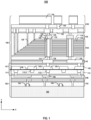
- FIG. 1 illustrates a cross-section of an exemplary bonded semiconductor device 100, according to some embodiments of the present disclosure.
- bonded semiconductor device 100 will be described as a non-monolithic 3D memory device.
- bonded semiconductor device 100 is not limited to a 3D memory device and can include any suitable bonded semiconductor devices that can use dummy bonding contacts to improve bonding interface properties as described below in detail. It is understood that bonded semiconductor devices that include dummy bonding contacts at its bonding interface as disclosed herein are not limited to the examples shown in FIG.
- DRAM dynamic random-access memory
- SRAM static random-access memory
- Flash memory non-volatile memory devices
- Bonded semiconductor device 100 represents an example of a non-monolithic 3D memory device.
- the term "non-monolithic” means that the components of bonded semiconductor device 100 (e.g., peripheral devices and memory array devices) can be formed separately on different substrates and then bonded to form a bonded semiconductor device.
- Bonded semiconductor device 100 can include a substrate 102, which can include silicon (e.g., single crystalline silicon), silicon germanium (SiGe), gallium arsenide (GaAs), germanium (Ge), silicon on insulator (SOI), or any other suitable materials.
- silicon e.g., single crystalline silicon
- SiGe silicon germanium
- GaAs gallium arsenide
- Ge germanium
- SOI silicon on insulator
- Substrate 102 includes two lateral surfaces (e.g., a top surface and a bottom surface) extending laterally in the x-direction (i.e., the lateral direction).
- one component e.g., a layer or a device
- another component e.g., a layer or a device
- the substrate of the semiconductor device e.g., substrate 102
- the y -direction i.e., the vertical direction
- Bonded semiconductor device 100 can include two semiconductor structures, i.e., a memory array device chip 160 and a peripheral device chip 162 bonded in a face-to-face manner at a bonding interface 158.
- bonding interface 158 is disposed between memory array device chip 160 and peripheral device chip 162 as a result of hybrid bonding (also known as "metal/dielectric hybrid bonding"), which is a direct bonding technology (e.g., forming bonding between surfaces without using intermediate layers, such as solder or adhesives) and can obtain metal-metal bonding and dielectric-dielectric bonding simultaneously.
- bonding interface 158 is the place at which memory array device chip 160 and peripheral device chip 162 are met and bonded.
- bonding interface 158 can be a layer with a certain thickness that includes the bottom surface of memory array device chip 160 and the bottom surface of peripheral device chip 162. It is understood that although memory array device chip 160 is disposed above peripheral device chip 162 in FIG. 1 , their relative positions can be reversed in some embodiments. For example, memory array device chip 160 can be disposed below peripheral device chip 162 in another bonded semiconductor device.
- Peripheral device chip 162 can include a peripheral device layer 103 on substrate 102.
- Peripheral device layer 103 can include a peripheral device (e.g., a plurality of transistors 104) formed on substrate 102.
- Transistors 104 can be formed "on" substrate 102, where the entirety or part of each transistor 104 is formed in substrate 102 (e.g., below the top surface of substrate 102) and/or directly on substrate 102.
- Isolation regions e.g., shallow trench isolations (STIs), not shown
- doped regions e.g., source regions and drain regions of transistors 104, not shown
- the peripheral device of peripheral device layer 103 can include any suitable digital, analog, and/or mixed-signal peripheral circuits used for facilitating the operation of bonded semiconductor device 100.
- the peripheral device of peripheral device layer 103 can include one or more of a page buffer, a decoder (e.g., a row decoder and a column decoder), a sense amplifier, a driver, a charge pump, a current or voltage reference, or any active or passive components of the circuits (e.g., transistors, diodes, resistors, or capacitors).
- the peripheral device of peripheral device layer 103 is formed on substrate 102 using complementary metal-oxide-semiconductor (CMOS) technology (also known as a "CMOS chip").
- CMOS complementary metal-oxide-semiconductor
- Peripheral device chip 162 can include an interconnect layer 106 (referred to herein as a "peripheral interconnect layer”) above peripheral device layer 103 to transfer electrical signals to and from peripheral device layer 103.
- Peripheral interconnect layer 106 can include a plurality of interconnects 108 (also referred to herein as "contacts"), including lateral interconnect lines and vertical interconnect access (via) contacts.
- interconnects can broadly include any suitable types of interconnects, such as middle-end-of-line (MEOL) interconnects and back-end-of-line (BEOL) interconnects.
- interconnects 108 in peripheral interconnect layer 106 can include functional interconnects that are electrically connected to the peripheral device and optionally, further include dummy interconnects that are not electrically connected to any peripheral device in peripheral device layer 103.
- Peripheral interconnect layer 106 can further include one or more interlayer dielectric (ILD) layers (also known as “intermetal dielectric (IMD) layers”) in which the interconnect lines and via contacts can form. That is, peripheral interconnect layer 106 can include interconnects 108 in multiple ILD layers.
- Interconnects 108 in peripheral interconnect layer 106 can include conductive materials including, but not limited to, tungsten (W), cobalt (Co), copper (Cu), aluminum (Al), silicides, or any combination thereof.
- the ILD layers in peripheral interconnect layer 106 can include dielectric materials including, but not limited to, silicon oxide, silicon nitride, silicon oxynitride, low dielectric constant (low-k) dielectrics, or any combination thereof.
- peripheral device chip 162 can further include a bonding layer 111 at bonding interface 158 and above peripheral interconnect layer 106 and peripheral device layer 103.
- Bonding layer 111 can include a plurality of bonding contacts 112 and a dielectric 113 electrically isolating bonding contacts 112.
- Bonding contacts 112 can include functional bonding contacts 112-1, each of which is part of an electrical connection between peripheral device chip 162 and memory array device chip 160.
- Bonding contacts 112 can also include dummy bonding contacts 112-2, each of which is not part of any electrical connection between peripheral device chip 162 and memory array device chip 160.
- bonding contacts 112 can include conductive materials including, but not limited to, W, Co, Cu, Al, silicides, or any combination thereof.
- the remaining area of bonding layer 111 can be formed with dielectric 113 including, but not limited to, silicon oxide, silicon nitride, silicon oxynitride, low-k dielectrics, or any combination thereof. Bonding contacts 112 and dielectric 113 in bonding layer 111 can be used for hybrid bonding as described below in detail.
- memory array device chip 160 is a NAND Flash memory device in which memory cells are provided in the form of an array of NAND memory strings 114 each extending vertically above peripheral device layer 103.
- Memory array device layer 120 can include NAND memory strings 114 that extend vertically through a plurality of pairs each including a conductor layer 116 and a dielectric layer 118 (referred to herein as "conductor/dielectric layer pairs").
- the stacked conductor/dielectric layer pairs are also referred to herein as a "memory stack.”
- Conductor layers 116 and dielectric layers 118 in the memory can stack alternately in the vertical direction.
- each NAND memory string 114 can include a semiconductor channel 124 and a dielectric layer (also known as a "memory film").
- semiconductor channel 124 includes silicon, such as amorphous silicon, polysilicon, or single crystalline silicon.
- the memory film is a composite layer including a tunneling layer 126, a storage layer 128 (also known as a "charge trap/storage layer”), and a blocking layer (not shown).
- Each NAND memory string 114 can have a cylinder shape (e.g., a pillar shape).
- Tunneling layer 126 can include silicon oxide, silicon oxynitride, or any combination thereof.
- Storage layer 128 can include silicon nitride, silicon oxynitride, silicon, or any combination thereof.
- the blocking layer can include silicon oxide, silicon oxynitride, high dielectric constant (high-k) dielectrics, or any combination thereof.
- NAND memory strings 114 further include a plurality of control gates (each being part of a word line). Each conductor layer 116 in the memory stack can act as a control gate for memory cell of each NAND memory string 114. Each NAND memory string 114 can include a source select gate at its upper end and a drain select gate at its lower end. As used herein, the "upper end" of a component (e.g., NAND memory string 114) is the end farther away from substrate 102 in the y -direction, and the "lower end" of the component (e.g., NAND memory string 114) is the end closer to substrate 102 in the y -direction.
- memory array device chip 160 further includes a semiconductor layer 130 disposed above and in contact with NAND memory strings 114.
- Memory array device layer 120 can be disposed below semiconductor layer 130.
- semiconductor layer 130 includes a plurality of semiconductor plugs 132 electrically separated by isolation regions.
- each semiconductor plug 132 is disposed at the upper end of corresponding NAND memory string 114 and functions as the drain of corresponding NAND memory string 114 and thus, can be considered as part of corresponding NAND memory string 114.
- Semiconductor plug 132 can include a single crystalline silicon.
- Semiconductor plug 132 can be un-doped, partially doped (in the thickness direction and/or the width direction), or fully doped by p-type or n-type dopants.
- memory array device chip 160 includes local interconnects that are formed in one or more ILD layers and in contact with components in memory array device layer 120, such as the word lines (e.g., conductor layers 116) and NAND memory strings 114.
- the local interconnects can include word line via contacts 136, source line via contacts 138, and bit line via contacts 140.
- Each local interconnect can include conductive materials including, but not limited to, W, Co, Cu, Al, silicides, or any combination thereof.
- Word line via contacts 136 can extend vertically through one or more ILD layers. Each word line via contact 136 can be in contact with corresponding conductor layer 116 to individually address a corresponding word line of bonded semiconductor device 100.
- Each source line via contact 138 can be in contact with the source of corresponding NAND memory string 114.
- Bit line via contacts 140 can extend vertically through one or more ILD layers. Each bit line via contact 140 can electrically connect to corresponding semiconductor plug 132 (e.g., the drain) of NAND memory string 114 to individually address corresponding NAND memory string 114.
- memory array device chip 160 can also include interconnect layers for transferring electrical signals to and from NAND memory strings 114.
- memory array device chip 160 can include an interconnect layer 142 (referred to herein as an "array interconnect layer") below memory array device layer 120.
- Array interconnect layer 142 can include a plurality of interconnects 144, including interconnect lines and via contacts in one or more ILD layers.
- interconnects 144 in array interconnect layer 142 can include functional interconnects that are electrically connected to NAND memory string 114 and optionally, further include dummy interconnects that are not electrically connected to any NAND memory string 114 in memory array device layer 120.
- memory array device chip 160 can further include a bonding layer 147 at bonding interface 158 and below array interconnect layer 142 and memory array device layer 120.
- Bonding layer 147 can include a plurality of bonding contacts 148 and a dielectric 149 electrically isolating bonding contacts 148.
- Bonding contacts 148 can include functional bonding contacts 148-1, each of which is part of an electrical connection between peripheral device chip 162 and memory array device chip 160.
- Bonding contacts 148 can also include dummy bonding contacts 148-2, each of which is not part of any electrical connection between peripheral device chip 162 and memory array device chip 160.
- bonding contacts 148-2 can be used for increasing the local density of bonding contacts 148 at bonding interface 158 to increase bonding yield and strength.
- Bonding contacts 148 can include conductive materials including, but not limited to, W, Co, Cu, Al, silicides, or any combination thereof.
- the remaining area of bonding layer 147 can be formed with dielectric 149 including, but not limited to, silicon oxide, silicon nitride, silicon oxynitride, low-k dielectrics, or any combination thereof. Bonding contacts 148 and dielectric 149 in bonding layer 147 can be used for hybrid bonding as described below in detail.
- another interconnect layer 150 can be disposed above memory array device layer 120 and can include interconnects, such as interconnect lines 152 and via contacts 154 in one or more ILD layers.
- BEOL interconnect layer 150 can further include contact pads 156 and a redistribution layer (not shown) at the top portion of bonded semiconductor device 100 for wire bonding and/or bonding with an interposer.
- BEOL interconnect layer 150 and array interconnect layer 142 can be formed on opposite sides of memory array device layer 120.
- interconnect lines 152, via contacts 154, and contact pads 156 in BEOL interconnect layer 150 can transfer electrical signals between bonded semiconductor device 100 and external circuits.
- bonding interface 158 can be formed between bonding layers 111 and 147.
- Bonding contacts 112 are in contact with bonding contacts 148 at bonding interface 158, and dielectric 113 is in contact with dielectric 149, according to some embodiments.
- a pair of functional bonding contacts 112-1 and 148-1 are in contact with one another at bonding interface 158, and pair of functional bonding contacts 112-1 and 148-1 are in contact with a pair of interconnects 108 and 144 on opposite sides of bonding interface 158, respectively.
- a pair of dummy bonding contacts 112-2 and 148-2 are in contact with one another at bonding interface 158 as well.
- dummy bonding contacts 112-2 and 148-2 in pair are separated from the functional interconnects on at least one side of bonding interface 158 (e.g., in peripheral interconnect layer 106 and/or array interconnect layer 142) to avoid forming an electrical connection between memory array device chip 160 and peripheral device chip 162.
- peripheral interconnect layer 106 and array interconnect layer 142 include a pair of dummy interconnects that are not electrically connected to NAND memory strings 114 and transistors 104, and pair of dummy bonding contacts 112-2 and 148-2 can be in contact with the pair of dummy interconnects on the opposite sides of bonding interface 158, respectively, without forming an electrical connection between memory array device chip 160 and peripheral device chip 162.
- a pair of dielectrics 113 and 149 are in contact with one another at bonding interface 158 as well.
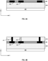
- FIGs. 2A and 2B illustrate cross-sections of various exemplary bonded semiconductor devices including dummy bonding contacts, according to various embodiments of the present disclosure.
- FIG. 2A illustrates a bonded structure 200 including a first semiconductor structure 202 and a second semiconductor structure 204, according to some embodiments.
- first semiconductor structure 202 is disposed below second semiconductor structure 204 in bonded structure 200 and includes a substrate 206, according to some embodiments.
- First semiconductor structure 202 can also include a first device layer 208 above substrate 206.
- first semiconductor structure 202 is a peripheral device chip or a memory array device chip, and first device layer 208 includes a peripheral device or a NAND memory string, respectively, as described above in FIG. 1 .
- second semiconductor structure 204 can include a second device layer 222.
- second semiconductor structure 204 is a memory array device chip or a peripheral device chip
- second device layer 222 includes a NAND memory string or a peripheral device, respectively, as described above in FIG. 1 .
- Bonded structure 200 can further include a bonding interface 203 between first and second semiconductor structures 202 and 204. It is understood that bonded structure 200 can include any other suitable semiconductor devices, such as logic devices, volatile memory devices (e.g., dynamic random-access memory (DRAM) and static random-access memory (SRAM)), and non-volatile memory devices (e.g., Flash memory), in a 2D, 2.5D, or 3D architecture.
- DRAM dynamic random-access memory
- SRAM static random-access memory
- Flash memory non-volatile memory devices
- First semiconductor structure 202 can further include a first bonding layer 216 above first interconnect layer 210.
- First bonding layer 216 includes bonding contacts 218 and 220 in one ILD layer, according to some embodiments.
- first bonding layer 216 can be formed by a single patterning process (e.g., involving only one photolithography and development process) in a single ILD layer.
- each bonding contact 218 or 220 has a nominally same critical dimension (e.g., the diameter of a via contact).
- each bonding contact 218 or 220 is a single damascene contact, as opposed to a dual damascene contact.
- first bonding layer 216 Two types of bonding contacts 218 and 220 can be formed in first bonding layer 216 depending on whether it is part of an electrical connection between first and second semiconductor structures 202 and 204.
- each bonding contact 218 is a functional bonding contact that is part of an electrical connection across bonding interface 203 and between first and second semiconductor structures 202 and 204.
- bonding contact 220 is a dummy bonding contact that is not part of an electrical connection across bonding interface 203 and between first and second semiconductor structures 202 and 204.
- Bonding contacts 218 and 220 in first bonding layer 216 can include conductive materials including, but not limited to, W, Co, Cu, Al, or any combination thereof.
- bonding contacts 218 and 220 are made of Cu for hybrid bonding.
- the density of bonding contacts can affect the hybrid bonding.
- the density of bonding contacts can be increased to improve the hybrid bonding yield and strength by adding dummy bonding contacts 220 in first bonding layer 216.
- each of interconnects 212 and 214 is in contact with a respective one of bonding contacts 218 and 220.
- interconnects 212 and 214 in first interconnect layer 210 and bonding contacts 218 and 220 in first bonding layer 216 have a one-to-one mapping relationship, and the number of bonding contacts 218 and 220 in first bonding layer 216 is the same as the number of interconnects 212 and 214 in first interconnect layer 210.
- Each interconnect 212 or 214 can act as an etch stop layer for forming corresponding bonding contact 218 or 220. In the areas without underneath interconnects 212 and 214, no bonding contact 218 or 220 is formed due to the lack of underneath etch stop layers (and all the bonding contacts 218 and 220 in first bonding layer 216 are formed by a single patterning process), according to some embodiments.
- First bonding layer 216 can further include dielectrics 221 between and electrically isolating bonding contacts 218 and 220.
- Dielectrics 221 in first bonding layer 216 can include dielectric materials including, but not limited to, silicon oxide, silicon nitride, silicon oxynitride, low-k dielectrics, or any combination thereof. In some embodiments, dielectrics 221 are made of silicon oxide for hybrid bonding.
- second semiconductor structure 204 can also include a second interconnect layer 224 below second device layer 222.
- Second interconnect layer 224 includes interconnects 226 and 228 in one or more ILD layers, according to some embodiments. Two types of interconnects 226 and 228 can be formed in second interconnect layer 224 depending on their functionalities.
- each interconnect 226 is a functional MEOL or BEOL interconnect (e.g., interconnect line or via contact) that is electrically connected to both first device layer 208 of first semiconductor structure 202 and second device layer 222 of second semiconductor structure 204 to transfer electrical signals across bonding interface 203 and between first and second semiconductor structure 202 and 204.
- Interconnect 228 can be a functional MEOL or BEOL interconnect (e.g., interconnect line or via contact) that is electrically connected to second device layer 222 of second semiconductor structure 204, but not first device layer 208 of first semiconductor structure 202, to transfer electrical signals within second semiconductor structure 204.
- interconnect 228 is a dummy interconnect that is not electrically connected to second device layer 222 of second semiconductor structure 204.
- Interconnects 226 and 228 in second interconnect layer 224 can include conductive materials including, but not limited to, W, Co, Cu, Al, silicides, or any combination thereof.
- the ILD layers in second interconnect layer 224 can include dielectric materials including, but not limited to, silicon oxide, silicon nitride, silicon oxynitride, low-k dielectrics, or any combination thereof.
- Second semiconductor structure 204 can further include a second bonding layer 230 below second interconnect layer 224.
- Second bonding layer 230 includes bonding contacts 232, 234, and 236 in two ILD layers, according to some embodiments. Different from first bonding layer 216, second bonding layer 230 can be formed by two patterning processes (e.g., two photolithography and development processes). As a result, bonding contacts 232, 234, and 236 in second bonding layer 230 can be formed in various designs. In some embodiments, bonding contacts 232 are dual damascene contacts, while bonding contacts 234 and 236 are single damascene contacts.
- bonding contact 232 can include a first portion 232-1 having a first critical dimension in one ILD layer and a second portion 232-2 having a second critical dimension different from the first critical dimension in another ILD layer.
- first portion 232-1 of bonding contact 232 can be in contact with corresponding interconnect 226 in second interconnect layer 224
- second portion 232-2 of bonding contact 232 can be in contact with corresponding bonding contact 218 on the opposite side of bonding interface 203.
- Bonding contact 232 thus can be in contact with corresponding interconnect 226 in second interconnect layer 224.
- bonding contacts 234 and 236 each does not include a first portion in contact with any interconnect in second interconnect layer 224, thereby being separated from interconnects 226 and 228 in second interconnect layer 224.
- bonding contacts 232, 234, and 236 can be formed in second bonding layer 230 depending on whether it is part of an electrical connection between first and second semiconductor structures 202 and 204.
- each bonding contact 232 is a functional bonding contact that is part of an electrical connection across bonding interface 203 and between first and second semiconductor structures 202 and 204.
- bonding contact 234 or 236 is a dummy bonding contact that is not part of an electrical connection across bonding interface 203 and between first and second semiconductor structures 202 and 204.
- Bonding contacts 232, 234, and 236 in second bonding layer 230 can include conductive materials including, but not limited to, W, Co, Cu, Al, or any combination thereof.
- bonding contacts 232, 234, and 236 are made of Cu for hybrid bonding.
- the density of bonding contacts can affect the hybrid bonding.
- the density of bonding contacts can be increased to improve the hybrid bonding yield and strength by adding dummy bonding contacts 234 in second bonding layer 230, which can form a high strength Cu-Cu fusion bonding with corresponding dummy bonding contacts 220 at bonding interface 203.
- dummy bonding contact 236 in second bonding layer 230 may not have a corresponding dummy bonding contact in first bonding layer 216 on the opposite side of bonding interface 203 due to the lack of an underneath interconnect in first interconnect layer 210 to act as the etch stop layer.
- each bonding contact 218 or 220 in first bonding layer 216 is in contact with a respective bonding contact 232 or 234 in second bonding layer 230 across bonding interface 203, while one or more bonding contacts (e.g., dummy bonding contact 236) in second bonding layer 230 is not in contact with any bonding contact in first bonding layer 216, according to some embodiments.
- the number of bonding contacts 232, 234, and 236 in second bonding layer 230 is greater than the number of bonding contacts 218 and 220 in first bonding layer 216.
- Second bonding layer 230 can further include dielectrics 237 between and electrically isolating bonding contacts 232, 234, and 236.
- Dielectrics 237 in second bonding layer 230 can include dielectric materials including, but not limited to, silicon oxide, silicon nitride, silicon oxynitride, low-k dielectrics, or any combination thereof. In some embodiments, dielectrics 237 are made of silicon oxide for hybrid bonding.
- a pair of functional bonding contacts 218 and 232 can be in contact with one another at bonding interface 203 and also in contact with a pair of interconnects 212 and 226 on opposite sides of bonding interface 203, respectively, to electrically connect the pair of interconnects 212 and 226.
- An electrical connection can thus be formed between the pair of interconnects 212 and 226 by the pair of functional bonding contacts 218 and 232.
- the pair of functional bonding contacts 218 and 232 also form a high strength Cu-Cu fusion bonding at bonding interface 203, according to some embodiments. On the other hand, in some embodiments.
- a pair of dummy bonding contacts 220 and 234 are in contact with one another at bonding interface 203 to form a high strength Cu-Cu fusion bonding at bonding interface 203 as well.
- the pair of dummy bonding contacts 220 and 234 are in contact with interconnect 214 (by dummy bonding contact 220) on one side of bonding interface 203 but separated from any interconnect 226 or 228 on the opposite side of bonding interface 203, according to some embodiments, thereby avoiding forming an electrical connection between interconnects across bonding interface 203.
- At least one dummy bonding contact 236 is separated from any bonding contact 218 or 220 at bonding interface 203, and a pair of dummy bonding contact 236 and dielectric 221 thus form a Cu-SiO 2 bonding at bonding interface 203.
- FIG. 2B illustrates a bonded structure 201 that is similar to bonded structure 200 illustrated in FIG. 2A except that the relative vertical positions of the components in first and second semiconductor structures 202 and 204 are switched.
- bonded structure 200 (except substrate 206) can be flipped vertically along bonding interface 203 to become bonded structure 201.
- dummy bonding contacts can be added to bonded structures 200 and 201 to increase bonding contacts density (and Cu-Cu fusion bonding in some embodiments) at bonding interface 203 to achieve better bonding performance.
- the design and arrangement of dummy bonding contacts can accommodate the reduction of total patterning processes in forming the dummy bonding contacts, thereby reducing the fabrication cost.
- the bonding contacts can be all single damascene contacts formed by a single patterning process.
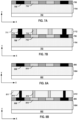
- FIG. 3 illustrates a cross-section of an exemplary bonded structure 300 including dummy bonding contacts and dummy interconnects, according to some embodiments of the present disclosure.
- bonding contacts on both sides of a bonding interface 303 between a first semiconductor structure 302 and a second semiconductor structure 304 can be single damascene contacts formed by a single patterning process.
- first semiconductor structure 302 is disposed below second semiconductor structure 304 in bonded structure 300 and includes a substrate 306, according to some embodiments.
- First semiconductor structure 302 can also include a first device layer 308 above substrate 306.
- first semiconductor structure 302 is a peripheral device chip or a memory array device chip, and first device layer 308 includes a peripheral device or a NAND memory string, respectively, as described above in FIG. 1 .
- second semiconductor structure 304 can include a second device layer 322.
- second semiconductor structure 304 is a memory array device chip or a peripheral device chip, and second device layer 322 includes a NAND memory string or a peripheral device, respectively, as described above in FIG. 1 .
- First semiconductor structure 302 can also include a first interconnect layer 310 above first device layer 308.
- First interconnect layer 310 includes interconnects 312 and 314 in one or more ILD layers, according to some embodiments. Two types of interconnects 312 and 314 can be formed in first interconnect layer 310 depending on their functionalities.
- each interconnect 312 is a functional MEOL or BEOL interconnect (e.g., interconnect line or via contact) that is electrically connected to both first device layer 308 of first semiconductor structure 302 and second device layer 322 of second semiconductor structure 304 to transfer electrical signals across bonding interface 303 and between first and second semiconductor structure 302 and 304.
- each interconnect 314 is a dummy interconnect that is not electrically connected to first device layer 308 (and the peripheral device or NAND memory string therein for example) of first semiconductor structure 302.
- dummy interconnects 314 can be added into first interconnect layer 310 in order to allow more dummy bonding contacts to be formed thereabove, thereby further increasing the bonding contact density at bonding interface 303.
- Interconnects 312 and 314 in first interconnect layer 310 can include conductive materials including, but not limited to, W, Co, Cu, Al, silicides, or any combination thereof.
- the ILD layers in first interconnect layer 310 can include dielectric materials including, but not limited to, silicon oxide, silicon nitride, silicon oxynitride, low-k dielectrics, or any combination thereof.
- First semiconductor structure 302 can further include a first bonding layer 316 above first interconnect layer 310.
- First bonding layer 316 includes bonding contacts 318 and 320 in one ILD layer, according to some embodiments.
- first bonding layer 316 can be formed by a single patterning process (e.g., involving only one photolithography and development process) in a single ILD layer.
- each bonding contact 318 or 320 has a nominally same critical dimension (e.g., the diameter of a via contact).
- each bonding contact 318 or 320 is a single damascene contact, as opposed to a dual damascene contact.
- first bonding layer 316 Two types of bonding contacts 318 and 320 can be formed in first bonding layer 316 depending on whether it is part of an electrical connection between first and second semiconductor structures 302 and 304.
- each bonding contact 318 is a functional bonding contact that is in contact with corresponding functional interconnect 312 and that is part of an electrical connection across bonding interface 303 and between first and second semiconductor structures 302 and 304.
- bonding contact 320 is a dummy bonding contact that is in contact with corresponding dummy interconnect 314 and that is not part of an electrical connection across bonding interface 303 and between first and second semiconductor structures 302 and 304.
- Bonding contacts 318 and 320 in first bonding layer 316 can include conductive materials including, but not limited to, W, Co, Cu, Al, or any combination thereof.
- bonding contacts 318 and 320 are made of Cu for hybrid bonding.
- interconnects 312 and 314 in first interconnect layer 310 and bonding contacts 318 and 320 in first bonding layer 316 have a one-to-one mapping relationship, and the number of bonding contacts 318 and 320 in first bonding layer 316 is the same as the number of interconnects 312 and 314 in first interconnect layer 310.
- Each interconnect 312 or 314 can act as an etch stop layer for forming corresponding bonding contact 318 or 320. In the areas without underneath interconnects 312 and 314, no bonding contact 318 or 320 is formed due to the lack of underneath etch stop layers (and all the bonding contacts 318 and 320 in first bonding layer 316 are formed by a single patterning process), according to some embodiments.
- First bonding layer 316 can further include dielectrics 321 between and electrically isolating bonding contacts 318 and 320.
- Dielectrics 321 in first bonding layer 316 can include dielectric materials including, but not limited to, silicon oxide, silicon nitride, silicon oxynitride, low-k dielectrics, or any combination thereof. In some embodiments, dielectrics 321 are made of silicon oxide for hybrid bonding.
- second semiconductor structure 304 can also include a second interconnect layer 324 below second device layer 322.
- Second interconnect layer 324 includes interconnects 326 and 328 in one or more ILD layers, according to some embodiments Two types of interconnects 326 and 328 can be formed in second interconnect layer 324 depending on their functionalities.
- each interconnect 326 is a functional MEOL or BEOL interconnect (e.g., interconnect line or via contact) that is electrically connected to both first device layer 308 of first semiconductor structure 302 and second device layer 322 of second semiconductor structure 304 to transfer electrical signals across bonding interface 303 and between first and second semiconductor structure 302 and 304.
- each interconnect 328 is a dummy interconnect that is not electrically connected to second device layer 322 (and the peripheral device or NAND memory string therein for example) of second semiconductor structure 304.
- dummy interconnects 328 can be added into second interconnect layer 324 in order to allow more dummy bonding contacts to be formed therebelow, thereby further increasing the bonding contact density at bonding interface 303.
- Interconnects 326 and 328 in second interconnect layer 324 can include conductive materials including, but not limited to, W, Co, Cu, Al, silicides, or any combination thereof.
- the ILD layers in second interconnect layer 324 can include dielectric materials including, but not limited to, silicon oxide, silicon nitride, silicon oxynitride, low-k dielectrics, or any combination thereof.
- Second semiconductor structure 304 can further include a second bonding layer 330 below second interconnect layer 324.
- second bonding layer 330 includes bonding contacts 332 and 334 in one ILD layer, according to some embodiments.
- second bonding layer 330 can be formed by a single patterning process (e.g., involving only one photolithography and development process) in a single ILD layer as well, just like first bonding layer 316 on the opposite side of bonding interface 303.
- each bonding contact 332 or 334 has a nominally same critical dimension (e.g., the diameter of a via contact).
- each bonding contact 332 or 334 is a single damascene contact, as opposed to a dual damascene contact. Two types of bonding contacts 332 and 334 can be formed in second bonding layer 330 depending on whether it is part of an electrical connection between first and second semiconductor structures 302 and 304. In some embodiments, each bonding contact 332 is a functional bonding contact that is in contact with corresponding functional interconnect 326 and that is part of an electrical connection across bonding interface 303 and between first and second semiconductor structures 302 and 304.
- bonding contact 334 is a dummy bonding contact that is in contact with corresponding dummy interconnect 328 and that is not part of an electrical connection across bonding interface 303 and between first and second semiconductor structures 302 and 304.
- Bonding contacts 332 and 334 in second bonding layer 330 can include conductive materials including, but not limited to, W, Co, Cu, Al, or any combination thereof. In some embodiments, bonding contacts 332 and 334 are made of Cu for hybrid bonding.
- the density of bonding contacts can affect the hybrid bonding.
- the density of bonding contacts can be increased to improve the hybrid bonding yield and strength by adding dummy interconnects 328 in second interconnect layer 324 and corresponding dummy bonding contacts 334 in second bonding layer 330.
- each of interconnects 326 and 328 is in contact with a respective one of bonding contacts 332 and 334.
- interconnects 326 and 328 in second interconnect layer 324 and bonding contacts 332 and 334 in second bonding layer 330 have a one-to-one mapping relationship, and the number of bonding contacts 332 and 334 in second bonding layer 330 is the same as the number of interconnects 326 and 328 in second interconnect layer 324.
- Each interconnect 326 or 328 can act as an etch stop layer for forming corresponding bonding contact 332 or 334. In the areas without underneath interconnects 326 and 328, no bonding contact 332 or 334 is formed due to the lack of underneath etch stop layers (and all the bonding contacts 332 and 334 in second bonding layer 330 are formed by a single patterning process), according to some embodiments.
- Second bonding layer 330 can further include dielectrics 335 between and electrically isolating bonding contacts 332 and 334.
- Dielectrics 335 in second bonding layer 330 can include dielectric materials including, but not limited to, silicon oxide, silicon nitride, silicon oxynitride, low-k dielectrics, or any combination thereof. In some embodiments, dielectrics 335 are made of silicon oxide for hybrid bonding.
- the number of bonding contacts in second bonding layer 230 may be greater than the number of bonding contacts in first bonding layer 216 (formed by a single patterning process)
- the number of bonding contacts 332 and 334 in second bonding layer 330 is the same as the number of bonding contacts in first bonding layer 316 (formed by a single patterning process).
- Each bonding contact 318 or 320 in first bonding layer 316 can be in contact with a respective bonding contact 332 or 334 in second bonding layer 330 at bonding interface 303.
- the bonding contacts on the opposite sides of bonding interface 303 have a one-to-one mapping relationship, according to some embodiments. Because functional bonding contacts 318 and 332 are paired and dummy bonding contacts 320 and 334 are paired as well, no bonding contact can be paired with dielectrics 321 or 335 to form, for example, a Cu-SiO 2 bonding. Consequently, the number of high strength Cu-Cu bondings can be further increased at bonding interface 303 to improve the bonding performance.
- a pair of functional bonding contacts 318 and 332 can be in contact with one another at bonding interface 303 and also in contact with a pair of functional interconnects 312 and 326 on opposite sides of bonding interface 303, respectively, to electrically connect the pair of functional interconnects 312 and 326.
- An electrical connection can thus be formed between the pair of functional interconnects 312 and 326 by the pair of functional bonding contacts 318 and 332.
- the pair of functional bonding contacts 318 and 332 also form a high strength Cu-Cu fusion bonding at bonding interface 303, according to some embodiments.
- a pair of dummy bonding contacts 320 and 334 are in contact with one another at bonding interface 303 to form a high strength Cu-Cu fusion bonding at bonding interface 303 as well.
- the pair of dummy bonding contacts 320 and 334 are in contact with a pair of dummy interconnects 314 and 328 on opposite sides of bonding interface 303, according to some embodiments.
- the remaining areas of first and second bonding layers 316 and 330 e.g., dielectrics 321 and 335, form a SiO 2 -SiO 2 covalent bonding at bonding interface 303.
- bonding contacts on each side of bonding interface 303 are nominally evenly disposed at bonding interface 303 in a plan view (not shown).
- the local density and/or global density of bonding contacts can be adjusted to accommodate various designs of bonded structure 300 by adding paired dummy interconnects and dummy contacts accordingly.
- bonded structure 200, 201, or 300 can include or be combined with other structures, such as device layer(s), interconnect layer(s), and substrate(s), to form any suitable semiconductor devices, for example, logic devices, volatile memory devices (e.g., dynamic random-access memory (DRAM) and static random-access memory (SRAM)), and non-volatile memory devices (e.g., Flash memory), in a 2D, 2.5D, or 3D architecture.
- DRAM dynamic random-access memory
- SRAM static random-access memory
- Flash memory non-volatile memory devices
- FIGs. 4A and 4B illustrate an exemplary fabrication process for forming a first semiconductor structure including dummy bonding contacts, according to some embodiments of the present disclosure.
- FIGs. 5A-5C illustrate an exemplary fabrication process for forming a second semiconductor structure including dummy bonding contacts, according to some embodiments of the present disclosure.
- FIG. 6 illustrates an exemplary fabrication process for bonding the first semiconductor structure and the second semiconductor structure, according to some embodiments of the present disclosure.
- FIG. 10 is a flowchart of a method for forming an exemplary bonded semiconductor device including dummy bonding contacts, according to some embodiments of the present disclosure. Examples of the bonded semiconductor device depicted in FIGs. 4-6 and 10 include bonded structures 200 and 201 depicted in FIGs.
- FIGs. 4-6 and 10 will be described together. It is understood that the operations shown in method 1000 are not exhaustive and that other operations can be performed as well before, after, or between any of the illustrated operations. Further, some of the operations may be performed simultaneously, or in a different order than shown in FIGs. 4-6 and 10 .
- method 1000 starts at operation 1002, in which a first interconnect layer including a plurality of first interconnects is formed above a first substrate.
- the first substrate can be a silicon substrate.
- a first device layer is formed between the first substrate and the first interconnect layer prior to forming the first interconnect layer.
- the first device layer can include a NAND memory string or a peripheral device.
- first device layer 404 is formed above a silicon substrate 402.
- first device layer 404 is a peripheral device layer including a plurality of transistors (not shown) formed on silicon substrate 402 by a plurality of processes including, but not limited to, photolithography, dry/wet etch, thin film deposition, thermal growth, implantation, CMP, and any other suitable processes.
- first device layer 404 is a memory array device layer including a plurality of NAND memory strings (not shown) each extending vertically through a memory stack (not shown) formed on silicon substrate 402.
- a dielectric stack including an alternating stack of sacrificial layers (e.g., silicon nitride) and dielectric layers (e.g., silicon oxide) can be formed on silicon substrate 402 by one or more thin film deposition processes including, but not limited to, CVD, physical vapor deposition (PVD), atomic layer deposition (ALD), or any combination thereof.
- the memory stack then can be formed on silicon substrate 402 by gate replacement processes, i.e., replacing the sacrificial layers in the dielectric stack with conductor layers.
- fabrication processes to form the NAND memory strings include forming a semiconductor channel that extends vertically through the dielectric stack, forming a composite dielectric layer (memory film) between the semiconductor channel and the dielectric stack, including, but not limited to, a tunneling layer, a storage layer, and a blocking layer.
- the semiconductor channel and the memory film can be formed by one or more thin film deposition processes such as ALD, CVD, PVD, any other suitable processes, or any combination thereof.
- first interconnect layer 406 is formed above first device layer 404.
- First interconnect layer 406 can include interconnects 408 and 410, including interconnect lines and via contacts in one or more ILD layers, to make electrical connections with first device layer 404.
- first interconnect layer 406 includes multiple ILD layers and interconnects therein formed by multiple processes.
- interconnects 408 and 410 can include conductive materials deposited by one or more thin film deposition processes including, but not limited to, CVD, PVD, ALD, electrochemical depositions, or any combination thereof.
- the ILD layers can include dielectric materials deposited by one or more thin film deposition processes including, but not limited to, CVD, PVD, ALD, or any combination thereof.
- Method 1000 proceeds to operation 1004, as illustrated in FIG. 6 , in which a first bonding layer including a plurality of first bonding contacts is formed above the first interconnect layer, such that each of the first interconnects is in contact with a respective one of the first bonding contacts.
- a first dielectric can be formed in the first bonding layer as well.
- the first bonding contacts in the first bonding layers are formed by a single patterning process.
- the number of the first bonding contacts is the same as the number of first interconnects.
- Each of the first bonding contacts has a nominally same critical dimension, according to some embodiments.
- a layer of dielectric 411 is deposited on the top surface of first interconnect layer 406 by a thin film deposition process including, but not limited to, CVD, PVD, ALD, or any combination thereof.
- Bonding contacts 414 and 416 are formed in dielectric 411 to form a first bonding layer 412 above first interconnect layer 406 and first device layer 404, according to some embodiments.
- Bonding contact 414 and 416 can be patterned by a single patterning process involving only one photolithography process.
- etch masks photoresist and/or hard masks
- Opening e.g., a via hole and/or a trench
- Bonding contacts 414 and 416 can include a barrier/adhesion layer and a conductor (e.g., a metal) deposited subsequently in this order by one or more thin film deposition processes including, but not limited to, CVD, PVD, ALD, electrochemical depositions, or any combination thereof, to fill the openings.
- the excess conductor can be removed by CMP, and the top surface of first bonding layer 412 can be planarized for bonding.
- Method 1000 proceeds to operation 1006, as illustrated in FIG. 10 , in which a second interconnect layer including a plurality of second interconnects is formed above a second substrate.
- the second substrate can be a silicon substrate.
- a second device layer is formed between the second substrate and the second interconnect layer prior to forming the second interconnect layer.
- the second device layer can include a peripheral device or a NAND memory string.
- second device layer 504 is formed above a silicon substrate 502.
- second device layer 504 is a memory array device layer including a plurality of NAND memory strings (not shown) each extending vertically through a memory stack (not shown) formed on silicon substrate 502. The details of forming the memory array device layer are described above and will not be repeated.
- second device layer 504 is a peripheral device layer including a plurality of transistors (not shown) formed on silicon substrate 502 by a plurality of processes including, but not limited to, photolithography, dry/wet etch, thin film deposition, thermal growth, implantation, CMP, and any other suitable processes.
- Second interconnect layer 506 is formed above second device layer 504.
- Second interconnect layer 506 can include interconnects 508, including interconnect lines and via contacts in one or more ILD layers, to make electrical connections with second device layer 504.
- second interconnect layer 506 includes multiple ILD layers and interconnects therein formed by multiple processes.
- interconnects 508 can include conductive materials deposited by one or more thin film deposition processes including, but not limited to, CVD, PVD, ALD, electrochemical depositions, or any combination thereof.
- the ILD layers can include dielectric materials deposited by one or more thin film deposition processes including, but not limited to, CVD, PVD, ALD, or any combination thereof.
- Method 1000 proceeds to operation 1008, as illustrated in FIG. 10 , in which a second bonding layer including a plurality of second bonding contacts is formed above the second interconnect layer, such that at least one of the second bonding contacts is in contact with a respective one of the second interconnects, and at least another one of the second bonding contacts is separated from the second interconnects.
- a second dielectric can be formed in the second bonding layer as well.
- the second bonding contacts in the second bonding layers are formed by two patterning processes.
- first portions of second bonding contacts are formed above the second interconnects by one of the two patterning processes, and second portions of second bonding contacts are formed above the first portions of second bonding contacts by another one of the two patterning processes.
- the number of the second portions of second bonding contacts is greater than the number of the first portions of second bonding contacts, according to some embodiments.
- a first layer of dielectric 509 is deposited on the top surface of second interconnect layer 506 by a thin film deposition process including, but not limited to, CVD, PVD, ALD, or any combination thereof.
- First portions of bonding contact 512-1 are formed in dielectric 509 to form a first bonding sub-layer 510-1 above second interconnect layer 506 and second device layer 504, according to some embodiments.
- First portions of bonding contact 512-1 can be patterned by a first patterning process involving one photolithography process.
- etch masks photoresist and/or hard masks
- Opening e.g., a via hole and/or a trench
- First portions of bonding contact 512-1 can include a barrier/adhesion layer and a conductor (e.g., a metal) deposited subsequently in this order by one or more thin film deposition processes including, but not limited to, CVD, PVD, ALD, electrochemical depositions, or any combination thereof, to fill the openings.
- the excess conductor can be removed by CMP, and the top surface of first bonding sub-layer 510-1 can be planarized.
- a second layer of dielectric 511 is deposited on the top surface of first bonding sub-layer 510-1 by a thin film deposition process including, but not limited to, CVD, PVD, ALD, or any combination thereof.
- Second portions of bonding contact 512-2 and 514 are formed in dielectric 511 to form a second bonding sub-layer 510-2 above first bonding sub-layer 510-1, according to some embodiments.
- First and second bonding sub-layers 510-1 and 510-2 can together be referred to here as a second bonding layer 510.
- Second portions of bonding contact 512-2 and 514 can be patterned by a second patterning process involving one photolithography process.
- etch masks are patterned by the second patterning process to expose dielectric 511 at the areas where first portions of bonding contacts 512-1 are formed underneath, such that first and second portions of bonding contacts 512-1 and 512-2 can together form a functional bonding contact electrically connected to underneath interconnects 508.
- etch masks photoresist and/or hard masks
- Second portions of bonding contacts 512-2 and 514 can include a barrier/adhesion layer and a conductor (e.g., a metal) deposited subsequently in this order by one or more thin film deposition processes including, but not limited to, CVD, PVD, ALD, electrochemical depositions, or any combination thereof, to fill the openings.
- a conductor e.g., a metal
- the excess conductor can be removed by CMP, and the top surface of second bonding layer 510 can be planarized for bonding.
- Method 1000 proceeds to operation 1010, as illustrated in FIG. 10 , in which the first substrate and the second substrate are bonded in a face-to-face manner, such that each of the first bonding contacts is in contact with one of the second bonding contacts at a bonding interface.
- the first dielectric can be in contact with the second dielectric as well after the bonding.
- the bonding can be hybrid bonding.
- Second bonding layer 510 facing down is to be bonded with first bonding layer 412 facing up, i.e., in a face-to-face manner.
- bonding contacts 414 and 416 are aligned with bonding contacts 512 and 514 prior to hybrid bonding, such that each bonding contact 414 or 416 is in contact with one of bonding contacts 512 and 514 at a bonding interface after the hybrid bonding, according to some embodiments.
- a treatment process e.g., a plasma treatment, a wet treatment, and/or a thermal treatment, is applied to the bonding surfaces prior to the hybrid bonding.
- bonding contacts 414 and 416 can be inter-mixed with bonding contacts 512 and 514, and dielectric 411 can be covalent-bonded with dielectric 511, thereby forming a bonding interface between first bonding layer 412 and second bonding layer 510.
- first bonding layer 412 is flipped upside down and is above second bonding layer 510 in the resulting bonded structure.
- first device layer 404 can be a peripheral device layer
- second device layer 504 can be a memory array device layer.
- first device layer 404 can be a memory array device layer
- second device layer 504 can be a peripheral device layer.
- first and second device layers 404 and 504 can be both peripheral device layers.
- first and second device layers 404 and 504 can be both memory array device layers.
- FIGs. 7A and 7B illustrate an exemplary fabrication process for forming a first semiconductor structure including dummy bonding contacts and dummy interconnects, according to some embodiments of the present disclosure.
- FIGs. 8A and 8B illustrate an exemplary fabrication process for forming a second semiconductor structure including dummy bonding contacts and dummy interconnects, according to some embodiments of the present disclosure.
- FIG. 9 illustrates another exemplary fabrication process for bonding the first semiconductor structure and the second semiconductor structure, according to some embodiments of the present disclosure.
- FIG. 11 is a flowchart of a method for forming an exemplary bonded semiconductor device including dummy bonding contacts and dummy interconnects, according to some embodiments of the present disclosure. Examples of the bonded semiconductor device depicted in FIGs.
- first device layer 704 is formed above a silicon substrate 702.
- first device layer 704 is a peripheral device layer including a plurality of transistors (not shown) formed on silicon substrate 702 by a plurality of processes including, but not limited to, photolithography, dry/wet etch, thin film deposition, thermal growth, implantation, CMP, and any other suitable processes.
- first device layer 704 is a memory array device layer including a plurality of NAND memory strings (not shown) each extending vertically through a memory stack (not shown) formed on silicon substrate 702. The details of forming the memory array device layer are described above and will not be repeated.
- first interconnect layer 706 is formed above first device layer 704.
- First interconnect layer 706 can include functional interconnects 708 and dummy interconnects 710, including interconnect lines and via contacts in one or more ILD layers.
- Functional interconnects 708 make electrical connections with first device layer 704, while dummy interconnects 710 are not electrically connected to first device layer 704, according to some embodiments.
- first interconnect layer 706 includes multiple ILD layers and interconnects therein formed by multiple processes.
- interconnects 708 and 710 can include conductive materials deposited by one or more thin film deposition processes including, but not limited to, CVD, PVD, ALD, electrochemical depositions, or any combination thereof.
- the ILD layers can include dielectric materials deposited by one or more thin film deposition processes including, but not limited to, CVD, PVD, ALD, or any combination thereof.
- Method 1100 proceeds to operation 1104, as illustrated in FIG. 11 , in which a first bonding layer including a plurality of first bonding contacts is formed above the first interconnect layer, such that each of the first interconnects is in contact with a respective one of the first bonding contacts.
- a first dielectric can be formed in the first bonding layer as well.
- the first bonding contacts in the first bonding layers are formed by a single patterning process.
- the number of the first bonding contacts is the same as the number of first interconnects.
- Each of the first bonding contacts has a nominally same critical dimension, according to some embodiments.
- a layer of dielectric 711 is deposited on the top surface of first interconnect layer 706 by a thin film deposition process including, but not limited to, CVD, PVD, ALD, or any combination thereof.
- Functional bonding contacts 714 and dummy bonding contacts 716 are formed in dielectric 711 to form a first bonding layer 712 above first interconnect layer 706 and first device layer 704, according to some embodiments.
- Bonding contacts 714 and 716 can be patterned by a single patterning process involving only one photolithography process.
- etch masks photoresist and/or hard masks
- etch masks are patterned by a single patterning process to expose dielectric 711 only at the areas where interconnects 708 and 710 are formed underneath. Opening (e.g., a via hole and/or a trench) then can be etched through first bonding layer 712 until being stopped by underneath interconnects 708 and 710 as etch stop layers using dry etch and/or wet etch.
- Bonding contacts 714 and 716 can include a barrier/adhesion layer and a conductor (e.g., a metal) deposited subsequently in this order by one or more thin film deposition processes including, but not limited to, CVD, PVD, ALD, electrochemical depositions, or any combination thereof, to fill the openings.
- a conductor e.g., a metal
- the excess conductor can be removed by CMP, and the top surface of first bonding layer 712 can be planarized for bonding.
- Method 1100 proceeds to operation 1106, as illustrated in FIG. 11 , in which a second interconnect layer including a plurality of second interconnects is formed above a second substrate.
- the second substrate can be a silicon substrate.
- At least one of the second interconnects can be at least one second dummy interconnect.
- a second device layer is formed between the second substrate and the second interconnect layer prior to forming the second interconnect layer.
- the second device layer can include a NAND memory string or a peripheral device.
- the second dummy interconnect is not electrically connected to the NAND memory string and the peripheral device, according to some embodiments.
- Second interconnect layer 806 can include functional interconnects 808 and dummy interconnects 810, including interconnect lines and via contacts in one or more ILD layers. Functional interconnects 808 make electrical connections with second device layer 804, while dummy interconnects 810 are not electrically connected to second device layer 804, according to some embodiments.
- second interconnect layer 806 includes multiple ILD layers and interconnects therein formed by multiple processes.
- interconnects 808 and 810 can include conductive materials deposited by one or more thin film deposition processes including, but not limited to, CVD, PVD, ALD, electrochemical depositions, or any combination thereof.
- the ILD layers can include dielectric materials deposited by one or more thin film deposition processes including, but not limited to, CVD, PVD, ALD, or any combination thereof.
- Method 1100 proceeds to operation 1108, as illustrated in FIG. 11 , in which a second bonding layer including a plurality of second bonding contacts is formed above the second interconnect layer, such that each of the second interconnects is in contact with a respective one of the second bonding contacts.
- a second dielectric can be formed in the second bonding layer as well.
- the second bonding contacts in the second bonding layers are formed by a single patterning process.
- the number of the second bonding contacts is the same as the number of the second interconnects.
- Each of the second bonding contacts has a nominally same critical dimension, according to some embodiments.
- the number of the second bonding contacts is the same as the number of the first bonding contacts.
- a layer of dielectric 811 is deposited on the top surface of second interconnect layer 806 by a thin film deposition process including, but not limited to, CVD, PVD, ALD, or any combination thereof.
- Functional bonding contacts 814 and dummy bonding contacts 816 are formed in dielectric 811 to form a second bonding layer 812 above second interconnect layer 806 and second device layer 804, according to some embodiments. Bonding contacts 814 and 816 can be patterned by a single patterning process involving only one photolithography process.
- etch masks photoresist and/or hard masks
- etch masks are patterned by a single patterning process to expose dielectric 811 only at the areas where interconnects 808 and 810 are formed underneath. Opening (e.g., a via hole and/or a trench) then can be etched through second bonding layer 812 until being stopped by underneath interconnects 808 and 810 as etch stop layers using dry etch and/or wet etch.
- Bonding contacts 814 and 816 can include a barrier/adhesion layer and a conductor (e.g., a metal) deposited subsequently in this order by one or more thin film deposition processes including, but not limited to, CVD, PVD, ALD, electrochemical depositions, or any combination thereof, to fill the openings.
- a conductor e.g., a metal
- the excess conductor can be removed by CMP, and the top surface of second bonding layer 812 can be planarized for bonding.
- Method 1100 proceeds to operation 1110, as illustrated in FIG. 11 , in which the first substrate and the second substrate are bonded in a face-to-face manner, such that each of the first bonding contacts is in contact with a respective one of the second bonding contacts at a bonding interface.
- the first dielectric can be in contact with the second dielectric as well after the bonding.
- the bonding can be hybrid bonding.
- silicon substrate 702 and first device layer 704 formed thereon are flipped upside down.
- First bonding layer 712 facing down is to be bonded with second bonding layer 812 facing up, i.e., in a face-to-face manner.
- bonding contacts 714 and 716 are aligned with bonding contacts 814 and 816 prior to hybrid bonding, such that each bonding contact 714 or 716 is in contact with corresponding bonding contact 814 or 816 at a bonding interface after the hybrid bonding, according to some embodiments.
- a treatment process e.g., a plasma treatment, a wet treatment, and/or a thermal treatment, is applied to the bonding surfaces prior to the hybrid bonding.
- bonding contacts 714 and 716 can be inter-mixed with bonding contacts 814 and 816, and dielectric 711 can be covalent-bonded with dielectric 811, thereby forming a bonding interface between first bonding layer 712 and second bonding layer 812.
- a semiconductor device includes a first semiconductor structure and a second semiconductor structure.
- the first semiconductor structure includes a first interconnect layer including a plurality of first interconnects. At least one of the first interconnects is at least one first dummy interconnect.
- the first semiconductor structure further includes a first bonding layer including a plurality of first bonding contacts. Each of the first interconnects is in contact with a respective one of the first bonding contacts.
- the second semiconductor structure includes a second interconnect layer including a plurality of second interconnects. At least one of the second interconnects is at least one second dummy interconnect.
- the second semiconductor structure further includes a second bonding layer including a plurality of second bonding contacts.
- the semiconductor device further includes a bonding interface between the first bonding layer and the second bonding layer.
- Each of the first bonding contacts is in contact with a respective one of the second bonding contacts at the bonding interface.
- a number of the first bonding contacts is the same as a number of first interconnects, and a number of the first bonding contacts is the same as a number of the first interconnects.
- a number of the first dummy interconnects is the same as a number of the second dummy interconnects.
- each of the first bonding contacts has a nominally same first critical dimension
- each of the second bonding contacts has a nominally same second critical dimension
- the first and second bonding contacts include a pair of dummy bonding contacts in contact with one another at the bonding interface, and the pair of dummy bonding contacts electrically connect a respective pair of first and second dummy interconnects.
- the first bonding layer further includes a first dielectric
- the second bonding layer further includes a second dielectric in contact with the first dielectric at the bonding interface.
- the first bonding contacts are nominally evenly disposed at the bonding interface, and the second bonding contacts are nominally evenly disposed at the bonding interface.
- one of the first semiconductor structure and the second semiconductor structure further includes a device layer having a NAND memory string, and another one of the first semiconductor structure and the second semiconductor structure further includes a device layer having a peripheral device.
- the first and second dummy interconnects are not electrically connected to the NAND memory string and the peripheral device.
- a bonded structure includes a bonding interface, a pair of functional bonding contacts, and a pair of dummy bonding contacts.
- the pair of functional bonding contacts are in contact with one another at the bonding interface.
- the pair of bonding contacts are in contact with a pair of functional interconnects on opposite sides of the bonding interface, respectively.
- the pair of dummy bonding contacts are in contact with one another at the bonding interface.
- the pair of dummy bonding contacts are in contact with a pair of dummy interconnects on the opposite sides of the bonding interface, respectively.
- the bonded structure further includes a pair of dielectrics in contact with one another at the bonding interface.
- a method for forming a semiconductor device is disclosed.
- a first interconnect layer including a plurality of first interconnects is formed above a first substrate. At least one of the first interconnects is at least one first dummy interconnect.
- a first bonding layer including a plurality of first bonding contacts is formed above the first interconnect layer, such that each of the first interconnects is in contact with a respective one of the first bonding contacts.
- a second interconnect layer including a plurality of second interconnects is formed above a second substrate. At least one of the second interconnects is at least one second dummy interconnect.
- a second bonding layer including a plurality of second bonding contacts is formed above the second interconnect layer, such that each of the second interconnects is in contact with a respective one of the second bonding contacts.
- the first substrate and the second substrate are bonded in a face-to-face manner, such that each of the first bonding contacts is in contact with a respective one of the second bonding contacts at a bonding interface.
- the first bonding contacts are formed by a single patterning process. In some embodiments, to form the second bonding layer, the second bonding contacts are formed by a single patterning process.
- a number of the first bonding contacts is the same as a number of first interconnects, and a number of the first bonding contacts is the same as a number of first interconnects.
- each of the first bonding contacts has a nominally same first critical dimension
- each of the second bonding contacts has a nominally same second critical dimension
- a first dielectric is formed in the first bonding layer.
- a second dielectric is formed in the second bonding layer. The first dielectric is in contact with the second dielectric at the bonding interface after the bonding, according to some embodiments.
- a first device layer having a NAND memory string is formed between the first interconnect layer and the first substrate, and a second device layer having a peripheral device between the second interconnect layer and the second substrate.
- the first and second dummy interconnects are not electrically connected to the NAND memory string and the peripheral device, according to some embodiments.
- a first device layer having a peripheral device is formed between the first interconnect layer and the first substrate, and a second device layer having a NAND memory string between the second interconnect layer and the second substrate.
- the first and second dummy interconnects are not electrically connected to the NAND memory string and the peripheral device, according to some embodiments.
- the bonding includes hybrid bonding.
Landscapes
- Internal Circuitry In Semiconductor Integrated Circuit Devices (AREA)
- Engineering & Computer Science (AREA)
- Manufacturing & Machinery (AREA)
- Semiconductor Memories (AREA)
- Non-Volatile Memory (AREA)
- Semiconductor Integrated Circuits (AREA)
Priority Applications (1)
| Application Number | Priority Date | Filing Date | Title |
|---|---|---|---|
| EP25170040.7A EP4567887A3 (fr) | 2019-01-30 | 2019-01-30 | Liaison hybride utilisant des contacts de liaison factices et des interconnexions factices |
Applications Claiming Priority (3)
| Application Number | Priority Date | Filing Date | Title |
|---|---|---|---|
| PCT/CN2019/073909 WO2020154954A1 (fr) | 2019-01-30 | 2019-01-30 | Soudage hybride au moyen de contacts de soudage factices et d'interconnexions factices |
| EP25170040.7A EP4567887A3 (fr) | 2019-01-30 | 2019-01-30 | Liaison hybride utilisant des contacts de liaison factices et des interconnexions factices |
| EP19913951.0A EP3850663A4 (fr) | 2019-01-30 | 2019-01-30 | Soudage hybride au moyen de contacts de soudage factices et d'interconnexions factices |
Related Parent Applications (1)
| Application Number | Title | Priority Date | Filing Date |
|---|---|---|---|
| EP19913951.0A Division EP3850663A4 (fr) | 2019-01-30 | 2019-01-30 | Soudage hybride au moyen de contacts de soudage factices et d'interconnexions factices |
Publications (2)
| Publication Number | Publication Date |
|---|---|
| EP4567887A2 true EP4567887A2 (fr) | 2025-06-11 |
| EP4567887A3 EP4567887A3 (fr) | 2025-08-27 |
Family
ID=66938506
Family Applications (2)
| Application Number | Title | Priority Date | Filing Date |
|---|---|---|---|
| EP19913951.0A Ceased EP3850663A4 (fr) | 2019-01-30 | 2019-01-30 | Soudage hybride au moyen de contacts de soudage factices et d'interconnexions factices |
| EP25170040.7A Pending EP4567887A3 (fr) | 2019-01-30 | 2019-01-30 | Liaison hybride utilisant des contacts de liaison factices et des interconnexions factices |
Family Applications Before (1)
| Application Number | Title | Priority Date | Filing Date |
|---|---|---|---|
| EP19913951.0A Ceased EP3850663A4 (fr) | 2019-01-30 | 2019-01-30 | Soudage hybride au moyen de contacts de soudage factices et d'interconnexions factices |
Country Status (7)
| Country | Link |
|---|---|
| US (2) | US10748851B1 (fr) |
| EP (2) | EP3850663A4 (fr) |
| JP (1) | JP7329601B2 (fr) |
| KR (1) | KR102618755B1 (fr) |
| CN (2) | CN111564424A (fr) |
| TW (1) | TWI694597B (fr) |
| WO (1) | WO2020154954A1 (fr) |
Families Citing this family (43)
| Publication number | Priority date | Publication date | Assignee | Title |
|---|---|---|---|---|
| US11018133B2 (en) * | 2009-10-12 | 2021-05-25 | Monolithic 3D Inc. | 3D integrated circuit |
| US11244916B2 (en) * | 2018-04-11 | 2022-02-08 | Invensas Bonding Technologies, Inc. | Low temperature bonded structures |
| US11158552B2 (en) | 2018-12-26 | 2021-10-26 | AP Memory Technology Corp. | Semiconductor device and method to manufacture the same |
| US11380614B2 (en) | 2018-12-26 | 2022-07-05 | AP Memory Technology Corp. | Circuit assembly |
| US11417628B2 (en) * | 2018-12-26 | 2022-08-16 | Ap Memory Technology Corporation | Method for manufacturing semiconductor structure |
| US11672111B2 (en) | 2018-12-26 | 2023-06-06 | Ap Memory Technology Corporation | Semiconductor structure and method for manufacturing a plurality thereof |
| US10811402B2 (en) | 2018-12-26 | 2020-10-20 | AP Memory Technology Corp. | Memory device and microelectronic package having the same |
| US10804202B2 (en) * | 2019-02-18 | 2020-10-13 | Sandisk Technologies Llc | Bonded assembly including a semiconductor-on-insulator die and methods for making the same |
| US11373963B2 (en) | 2019-04-12 | 2022-06-28 | Invensas Bonding Technologies, Inc. | Protective elements for bonded structures |
| US11205625B2 (en) | 2019-04-12 | 2021-12-21 | Invensas Bonding Technologies, Inc. | Wafer-level bonding of obstructive elements |
| US11610846B2 (en) | 2019-04-12 | 2023-03-21 | Adeia Semiconductor Bonding Technologies Inc. | Protective elements for bonded structures including an obstructive element |
| US11385278B2 (en) | 2019-05-23 | 2022-07-12 | Invensas Bonding Technologies, Inc. | Security circuitry for bonded structures |
| CN110289221B (zh) * | 2019-06-25 | 2021-06-29 | 武汉新芯集成电路制造有限公司 | 一种半导体器件及其制造方法 |
| CN112864168B (zh) * | 2019-08-23 | 2023-05-02 | 长江存储科技有限责任公司 | 非易失性存储器件及其制造方法 |
| WO2021046744A1 (fr) * | 2019-09-11 | 2021-03-18 | Yangtze Memory Technologies Co., Ltd. | Dispositifs à semi-conducteurs liés ayant un processeur et une mémoire vive statique et leurs procédés de formation |
| CN110945650A (zh) | 2019-11-05 | 2020-03-31 | 长江存储科技有限责任公司 | 具有通过键合而形成的毗连通孔结构的半导体设备和用于形成其的方法 |
| CN111383992B (zh) * | 2020-03-23 | 2023-07-28 | 长江存储科技有限责任公司 | 半导体器件的制造方法 |
| CN113629048B (zh) * | 2020-05-07 | 2024-12-10 | 爱普科技股份有限公司 | 半导体结构及制造多个半导体结构的方法 |
| US12165947B2 (en) * | 2020-07-27 | 2024-12-10 | Taiwan Semiconductor Manufacturing Co., Ltd. | Semiconductor devices and method for forming the same |
| JP2022035158A (ja) * | 2020-08-20 | 2022-03-04 | キオクシア株式会社 | 半導体記憶装置 |
| US11688681B2 (en) * | 2020-08-24 | 2023-06-27 | Ap Memory Technology Corporation | DRAM chiplet structure and method for manufacturing the same |
| CN112071767B (zh) * | 2020-09-03 | 2024-05-07 | 长江存储科技有限责任公司 | 一种半导体器件及其检测方法 |
| WO2022067587A1 (fr) * | 2020-09-29 | 2022-04-07 | 华为技术有限公司 | Mémoire tridimensionnelle et son procédé de fabrication, et dispositif électronique |
| KR102934455B1 (ko) * | 2020-11-04 | 2026-03-09 | 삼성전자주식회사 | 반도체 장치 및 이를 포함하는 데이터 저장 시스템 |
| US11538778B2 (en) * | 2020-12-18 | 2022-12-27 | Advanced Semiconductor Engineering, Inc. | Semiconductor package including alignment material and method for manufacturing semiconductor package |
| CN113161362B (zh) * | 2021-03-15 | 2022-05-10 | 长江存储科技有限责任公司 | 三维存储器及其制作方法 |
| US12113042B2 (en) * | 2021-03-26 | 2024-10-08 | Taiwan Semiconductor Manufacturing Company, Ltd. | Metal bonding structure and manufacturing method thereof |
| CN113410223B (zh) * | 2021-06-15 | 2022-04-08 | 上海壁仞智能科技有限公司 | 芯片组及其制造方法 |
| CN117501443A (zh) * | 2021-06-15 | 2024-02-02 | 华为技术有限公司 | 芯片堆叠结构以及制作方法、晶圆堆叠结构、电子设备 |
| US12094849B2 (en) * | 2021-07-22 | 2024-09-17 | Taiwan Semiconductor Manufacturing Company, Ltd. | Atomic layer deposition bonding layer for joining two semiconductor devices |
| JP2024528964A (ja) | 2021-08-02 | 2024-08-01 | アデイア セミコンダクター ボンディング テクノロジーズ インコーポレイテッド | ボンデッド構造体用の保護半導体素子 |
| CN113764355B (zh) * | 2021-09-06 | 2023-12-05 | 长江存储科技有限责任公司 | 半导体结构 |
| JP2024538179A (ja) * | 2021-10-18 | 2024-10-18 | アデイア セミコンダクター テクノロジーズ リミテッド ライアビリティ カンパニー | 結合構造における寄生容量の低減 |
| EP4454008A4 (fr) * | 2021-12-23 | 2025-11-05 | Adeia Semiconductor Bonding Technologies Inc | Liaison directe sur des substrats de boîtier |
| CN114783984A (zh) * | 2022-04-22 | 2022-07-22 | 武汉新芯集成电路制造有限公司 | 三维集成装置及其制作方法 |
| CN114551409A (zh) * | 2022-04-28 | 2022-05-27 | 之江实验室 | 用于提高多芯粒晶圆集成可靠性的混合键合结构和方法 |
| CN115064518B (zh) * | 2022-05-23 | 2026-02-06 | 长江存储科技有限责任公司 | 半导体结构及制作方法、存储器、存储器系统和电子设备 |
| KR20240003600A (ko) | 2022-07-01 | 2024-01-09 | 삼성전자주식회사 | 더미 패드를 포함하는 반도체 장치 |
| KR20240015225A (ko) | 2022-07-26 | 2024-02-05 | 삼성전자주식회사 | 반도체 패키지 |
| US12577665B2 (en) * | 2022-08-23 | 2026-03-17 | Tokyo Electron Limited | Next generation bonding layer for 3D heterogeneous integration |
| WO2024102501A1 (fr) * | 2022-11-08 | 2024-05-16 | Peiching Ling | Structure semi-conductrice avec couche d'arrêt de gravure et son procédé de fabrication |
| US12550662B2 (en) | 2022-11-18 | 2026-02-10 | Applied Materials Inc. | Integrated process flows for hybrid bonding |
| CN118969765B (zh) * | 2023-05-06 | 2026-04-14 | 长鑫存储技术有限公司 | 键合结构及其形成方法、键合方法 |
Family Cites Families (32)
| Publication number | Priority date | Publication date | Assignee | Title |
|---|---|---|---|---|
| JP4121356B2 (ja) * | 2002-10-31 | 2008-07-23 | 富士通株式会社 | 半導体装置 |
| AU2002368524A1 (en) | 2002-12-20 | 2004-07-22 | International Business Machines Corporation | Three-dimensional device fabrication method |
| US7224069B2 (en) | 2005-07-25 | 2007-05-29 | Taiwan Semiconductor Manufacturing Company, Ltd. | Dummy structures extending from seal ring into active circuit area of integrated circuit chip |
| SG134187A1 (en) * | 2006-01-13 | 2007-08-29 | Tezzaron Semiconductor S Pte L | Stacked wafer for 3d integration |
| US8187897B2 (en) | 2008-08-19 | 2012-05-29 | International Business Machines Corporation | Fabricating product chips and die with a feature pattern that contains information relating to the product chip |
| JP5553693B2 (ja) | 2010-06-30 | 2014-07-16 | キヤノン株式会社 | 固体撮像装置及び撮像システム |
| KR101952976B1 (ko) * | 2011-05-24 | 2019-02-27 | 소니 주식회사 | 반도체 장치 |
| US8765598B2 (en) | 2011-06-02 | 2014-07-01 | Micron Technology, Inc. | Conductive structures, systems and devices including conductive structures and related methods |
| KR101428754B1 (ko) * | 2013-05-14 | 2014-08-11 | (주)실리콘화일 | 방열 특성이 개선된 반도체 장치 |
| JP6212720B2 (ja) | 2013-09-20 | 2017-10-18 | パナソニックIpマネジメント株式会社 | 半導体装置及びその製造方法 |
| TWI676279B (zh) | 2013-10-04 | 2019-11-01 | 新力股份有限公司 | 半導體裝置及固體攝像元件 |
| KR102320576B1 (ko) | 2013-12-27 | 2021-11-02 | 가부시키가이샤 한도오따이 에네루기 켄큐쇼 | 반도체 장치 |
| CN104779238B (zh) | 2014-01-10 | 2018-08-21 | 中芯国际集成电路制造(上海)有限公司 | 一种晶圆接合质量的检测结构及检测方法 |
| JP6195995B2 (ja) | 2014-02-26 | 2017-09-20 | インテル コーポレイション | ブリッジ貫通導電ビア信号接続を有する埋込マルチデバイスブリッジ |
| US9299736B2 (en) | 2014-03-28 | 2016-03-29 | Taiwan Semiconductor Manufacturing Company, Ltd. | Hybrid bonding with uniform pattern density |
| KR102287754B1 (ko) * | 2014-08-22 | 2021-08-09 | 삼성전자주식회사 | 칩 적층 반도체 패키지 |
| JP6203152B2 (ja) | 2014-09-12 | 2017-09-27 | 東芝メモリ株式会社 | 半導体記憶装置の製造方法 |
| US10418369B2 (en) * | 2015-10-24 | 2019-09-17 | Monolithic 3D Inc. | Multi-level semiconductor memory device and structure |
| CN111883501B (zh) * | 2015-05-18 | 2024-10-18 | 索尼公司 | 光检测装置和成像装置 |
| KR102500813B1 (ko) * | 2015-09-24 | 2023-02-17 | 삼성전자주식회사 | 반도체 소자 및 이의 제조 방법 |
| WO2017111792A1 (fr) | 2015-12-23 | 2017-06-29 | Intel Corporation | Fabrication et utilisation de trous d'interconnexion traversants en silicium sur un dispositif d'interconnexion à deux côtés |
| US9923011B2 (en) * | 2016-01-12 | 2018-03-20 | Taiwan Semiconductor Manufacturing Co., Ltd. | Semiconductor device structure with stacked semiconductor dies |
| US10050018B2 (en) * | 2016-02-26 | 2018-08-14 | Taiwan Semiconductor Manufacturing Company, Ltd. | 3DIC structure and methods of forming |
| JP6515046B2 (ja) | 2016-03-10 | 2019-05-15 | 東芝メモリ株式会社 | 半導体記憶装置 |
| US10141391B2 (en) * | 2017-02-23 | 2018-11-27 | International Business Machines Corporation | Microstructure modulation for 3D bonded semiconductor containing an embedded resistor structure |
| JP2018148071A (ja) | 2017-03-07 | 2018-09-20 | 東芝メモリ株式会社 | 記憶装置 |
| JP6963873B2 (ja) * | 2017-05-26 | 2021-11-10 | ソニーセミコンダクタソリューションズ株式会社 | 固体撮像素子、固体撮像素子の製造方法および電子機器 |
| CN107731667B (zh) * | 2017-08-28 | 2019-06-14 | 长江存储科技有限责任公司 | 具备金属连线的混合键合方法及混合键合结构 |
| CN107658317B (zh) | 2017-09-15 | 2019-01-01 | 长江存储科技有限责任公司 | 一种半导体装置及其制备方法 |
| CN107887395B (zh) * | 2017-11-30 | 2018-12-14 | 长江存储科技有限责任公司 | Nand存储器及其制备方法 |
| CN109219885A (zh) * | 2018-07-20 | 2019-01-15 | 长江存储科技有限责任公司 | 三维存储器件 |
| WO2020034063A1 (fr) * | 2018-08-13 | 2020-02-20 | Yangtze Memory Technologies Co., Ltd. | Contacts de soudage ayant une couche de capsulage et procédé destiné à les former |
-
2019
- 2019-01-30 EP EP19913951.0A patent/EP3850663A4/fr not_active Ceased
- 2019-01-30 CN CN202010446465.5A patent/CN111564424A/zh active Pending
- 2019-01-30 WO PCT/CN2019/073909 patent/WO2020154954A1/fr not_active Ceased
- 2019-01-30 EP EP25170040.7A patent/EP4567887A3/fr active Pending
- 2019-01-30 CN CN201980000243.6A patent/CN109891582B/zh active Active
- 2019-01-30 JP JP2021530781A patent/JP7329601B2/ja active Active
- 2019-01-30 KR KR1020217016068A patent/KR102618755B1/ko active Active
- 2019-03-04 US US16/292,279 patent/US10748851B1/en active Active
- 2019-03-13 TW TW108108365A patent/TWI694597B/zh active
-
2020
- 2020-07-08 US US16/924,042 patent/US11205619B2/en active Active
Also Published As
| Publication number | Publication date |
|---|---|
| US11205619B2 (en) | 2021-12-21 |
| WO2020154954A1 (fr) | 2020-08-06 |
| CN109891582B (zh) | 2020-06-26 |
| KR102618755B1 (ko) | 2023-12-27 |
| EP3850663A4 (fr) | 2023-07-12 |
| EP3850663A1 (fr) | 2021-07-21 |
| TW202029478A (zh) | 2020-08-01 |
| US10748851B1 (en) | 2020-08-18 |
| US20200243455A1 (en) | 2020-07-30 |
| KR20210086675A (ko) | 2021-07-08 |
| CN111564424A (zh) | 2020-08-21 |
| TWI694597B (zh) | 2020-05-21 |
| JP7329601B2 (ja) | 2023-08-18 |
| JP2022511451A (ja) | 2022-01-31 |
| US20200335450A1 (en) | 2020-10-22 |
| EP4567887A3 (fr) | 2025-08-27 |
| CN109891582A (zh) | 2019-06-14 |
Similar Documents
| Publication | Publication Date | Title |
|---|---|---|
| US11205619B2 (en) | Hybrid bonding using dummy bonding contacts and dummy interconnects | |
| US11462503B2 (en) | Hybrid bonding using dummy bonding contacts | |
| US11430756B2 (en) | Bonded semiconductor structures having bonding contacts made of indiffusible conductive materials and methods for forming the same | |
| US20230317665A1 (en) | Bonding contacts having capping layer and method for forming the same | |
| US11145645B2 (en) | Multi-stack three-dimensional memory devices | |
| US10580788B2 (en) | Methods for forming three-dimensional memory devices | |
| US10867678B2 (en) | Three-dimensional memory devices | |
| US12082411B2 (en) | Three-dimensional memory device with backside interconnect structures | |
| WO2020000392A1 (fr) | Dispositifs de type mémoires tridimensionnelles à puces de dispositif empilées utilisant des interposeurs |
Legal Events
| Date | Code | Title | Description |
|---|---|---|---|
| PUAI | Public reference made under article 153(3) epc to a published international application that has entered the european phase |
Free format text: ORIGINAL CODE: 0009012 |
|
| STAA | Information on the status of an ep patent application or granted ep patent |
Free format text: STATUS: REQUEST FOR EXAMINATION WAS MADE |
|
| 17P | Request for examination filed |
Effective date: 20250411 |
|
| AC | Divisional application: reference to earlier application |
Ref document number: 3850663 Country of ref document: EP Kind code of ref document: P |
|
| AK | Designated contracting states |
Kind code of ref document: A2 Designated state(s): AL AT BE BG CH CY CZ DE DK EE ES FI FR GB GR HR HU IE IS IT LI LT LU LV MC MK MT NL NO PL PT RO RS SE SI SK SM TR |
|
| PUAL | Search report despatched |
Free format text: ORIGINAL CODE: 0009013 |
|
| AK | Designated contracting states |
Kind code of ref document: A3 Designated state(s): AL AT BE BG CH CY CZ DE DK EE ES FI FR GB GR HR HU IE IS IT LI LT LU LV MC MK MT NL NO PL PT RO RS SE SI SK SM TR |
|
| RIC1 | Information provided on ipc code assigned before grant |
Ipc: H01L 25/065 20230101AFI20250723BHEP Ipc: H01L 23/00 20060101ALI20250723BHEP Ipc: H01L 25/00 20060101ALI20250723BHEP |
|
| STAA | Information on the status of an ep patent application or granted ep patent |
Free format text: STATUS: EXAMINATION IS IN PROGRESS |