EP4571845A1 - Cellule solaire, son procédé de préparation et module photovoltaïque - Google Patents
Cellule solaire, son procédé de préparation et module photovoltaïque Download PDFInfo
- Publication number
- EP4571845A1 EP4571845A1 EP24153724.0A EP24153724A EP4571845A1 EP 4571845 A1 EP4571845 A1 EP 4571845A1 EP 24153724 A EP24153724 A EP 24153724A EP 4571845 A1 EP4571845 A1 EP 4571845A1
- Authority
- EP
- European Patent Office
- Prior art keywords
- doped polysilicon
- layer
- structures
- substrate
- layers
- Prior art date
- Legal status (The legal status is an assumption and is not a legal conclusion. Google has not performed a legal analysis and makes no representation as to the accuracy of the status listed.)
- Pending
Links
Images


Classifications
-
- H—ELECTRICITY
- H10—SEMICONDUCTOR DEVICES; ELECTRIC SOLID-STATE DEVICES NOT OTHERWISE PROVIDED FOR
- H10F—INORGANIC SEMICONDUCTOR DEVICES SENSITIVE TO INFRARED RADIATION, LIGHT, ELECTROMAGNETIC RADIATION OF SHORTER WAVELENGTH OR CORPUSCULAR RADIATION
- H10F10/00—Individual photovoltaic cells, e.g. solar cells
- H10F10/10—Individual photovoltaic cells, e.g. solar cells having potential barriers
- H10F10/14—Photovoltaic cells having only PN homojunction potential barriers
-
- H—ELECTRICITY
- H10—SEMICONDUCTOR DEVICES; ELECTRIC SOLID-STATE DEVICES NOT OTHERWISE PROVIDED FOR
- H10F—INORGANIC SEMICONDUCTOR DEVICES SENSITIVE TO INFRARED RADIATION, LIGHT, ELECTROMAGNETIC RADIATION OF SHORTER WAVELENGTH OR CORPUSCULAR RADIATION
- H10F77/00—Constructional details of devices covered by this subclass
- H10F77/30—Coatings
- H10F77/306—Coatings for devices having potential barriers
- H10F77/311—Coatings for devices having potential barriers for photovoltaic cells
-
- H—ELECTRICITY
- H10—SEMICONDUCTOR DEVICES; ELECTRIC SOLID-STATE DEVICES NOT OTHERWISE PROVIDED FOR
- H10F—INORGANIC SEMICONDUCTOR DEVICES SENSITIVE TO INFRARED RADIATION, LIGHT, ELECTROMAGNETIC RADIATION OF SHORTER WAVELENGTH OR CORPUSCULAR RADIATION
- H10F77/00—Constructional details of devices covered by this subclass
- H10F77/10—Semiconductor bodies
- H10F77/14—Shape of semiconductor bodies; Shapes, relative sizes or dispositions of semiconductor regions within semiconductor bodies
-
- H—ELECTRICITY
- H10—SEMICONDUCTOR DEVICES; ELECTRIC SOLID-STATE DEVICES NOT OTHERWISE PROVIDED FOR
- H10F—INORGANIC SEMICONDUCTOR DEVICES SENSITIVE TO INFRARED RADIATION, LIGHT, ELECTROMAGNETIC RADIATION OF SHORTER WAVELENGTH OR CORPUSCULAR RADIATION
- H10F10/00—Individual photovoltaic cells, e.g. solar cells
- H10F10/10—Individual photovoltaic cells, e.g. solar cells having potential barriers
- H10F10/14—Photovoltaic cells having only PN homojunction potential barriers
- H10F10/146—Back-junction photovoltaic cells, e.g. having interdigitated base-emitter regions on the back side
-
- H—ELECTRICITY
- H10—SEMICONDUCTOR DEVICES; ELECTRIC SOLID-STATE DEVICES NOT OTHERWISE PROVIDED FOR
- H10F—INORGANIC SEMICONDUCTOR DEVICES SENSITIVE TO INFRARED RADIATION, LIGHT, ELECTROMAGNETIC RADIATION OF SHORTER WAVELENGTH OR CORPUSCULAR RADIATION
- H10F10/00—Individual photovoltaic cells, e.g. solar cells
- H10F10/10—Individual photovoltaic cells, e.g. solar cells having potential barriers
- H10F10/16—Photovoltaic cells having only PN heterojunction potential barriers
- H10F10/164—Photovoltaic cells having only PN heterojunction potential barriers comprising heterojunctions with Group IV materials, e.g. ITO/Si or GaAs/SiGe photovoltaic cells
- H10F10/165—Photovoltaic cells having only PN heterojunction potential barriers comprising heterojunctions with Group IV materials, e.g. ITO/Si or GaAs/SiGe photovoltaic cells the heterojunctions being Group IV-IV heterojunctions, e.g. Si/Ge, SiGe/Si or Si/SiC photovoltaic cells
-
- H—ELECTRICITY
- H10—SEMICONDUCTOR DEVICES; ELECTRIC SOLID-STATE DEVICES NOT OTHERWISE PROVIDED FOR
- H10F—INORGANIC SEMICONDUCTOR DEVICES SENSITIVE TO INFRARED RADIATION, LIGHT, ELECTROMAGNETIC RADIATION OF SHORTER WAVELENGTH OR CORPUSCULAR RADIATION
- H10F19/00—Integrated devices, or assemblies of multiple devices, comprising at least one photovoltaic cell covered by group H10F10/00, e.g. photovoltaic modules
- H10F19/90—Structures for connecting between photovoltaic cells, e.g. interconnections or insulating spacers
- H10F19/902—Structures for connecting between photovoltaic cells, e.g. interconnections or insulating spacers for series or parallel connection of photovoltaic cells
- H10F19/908—Structures for connecting between photovoltaic cells, e.g. interconnections or insulating spacers for series or parallel connection of photovoltaic cells for back-contact photovoltaic cells
-
- H—ELECTRICITY
- H10—SEMICONDUCTOR DEVICES; ELECTRIC SOLID-STATE DEVICES NOT OTHERWISE PROVIDED FOR
- H10F—INORGANIC SEMICONDUCTOR DEVICES SENSITIVE TO INFRARED RADIATION, LIGHT, ELECTROMAGNETIC RADIATION OF SHORTER WAVELENGTH OR CORPUSCULAR RADIATION
- H10F71/00—Manufacture or treatment of devices covered by this subclass
- H10F71/121—The active layers comprising only Group IV materials
- H10F71/1221—The active layers comprising only Group IV materials comprising polycrystalline silicon
-
- H—ELECTRICITY
- H10—SEMICONDUCTOR DEVICES; ELECTRIC SOLID-STATE DEVICES NOT OTHERWISE PROVIDED FOR
- H10F—INORGANIC SEMICONDUCTOR DEVICES SENSITIVE TO INFRARED RADIATION, LIGHT, ELECTROMAGNETIC RADIATION OF SHORTER WAVELENGTH OR CORPUSCULAR RADIATION
- H10F71/00—Manufacture or treatment of devices covered by this subclass
- H10F71/129—Passivating
-
- H—ELECTRICITY
- H10—SEMICONDUCTOR DEVICES; ELECTRIC SOLID-STATE DEVICES NOT OTHERWISE PROVIDED FOR
- H10F—INORGANIC SEMICONDUCTOR DEVICES SENSITIVE TO INFRARED RADIATION, LIGHT, ELECTROMAGNETIC RADIATION OF SHORTER WAVELENGTH OR CORPUSCULAR RADIATION
- H10F71/00—Manufacture or treatment of devices covered by this subclass
- H10F71/138—Manufacture of transparent electrodes, e.g. transparent conductive oxides [TCO] or indium tin oxide [ITO] electrodes
-
- H—ELECTRICITY
- H10—SEMICONDUCTOR DEVICES; ELECTRIC SOLID-STATE DEVICES NOT OTHERWISE PROVIDED FOR
- H10F—INORGANIC SEMICONDUCTOR DEVICES SENSITIVE TO INFRARED RADIATION, LIGHT, ELECTROMAGNETIC RADIATION OF SHORTER WAVELENGTH OR CORPUSCULAR RADIATION
- H10F77/00—Constructional details of devices covered by this subclass
- H10F77/10—Semiconductor bodies
- H10F77/12—Active materials
- H10F77/122—Active materials comprising only Group IV materials
- H10F77/1223—Active materials comprising only Group IV materials characterised by the dopants
-
- H—ELECTRICITY
- H10—SEMICONDUCTOR DEVICES; ELECTRIC SOLID-STATE DEVICES NOT OTHERWISE PROVIDED FOR
- H10F—INORGANIC SEMICONDUCTOR DEVICES SENSITIVE TO INFRARED RADIATION, LIGHT, ELECTROMAGNETIC RADIATION OF SHORTER WAVELENGTH OR CORPUSCULAR RADIATION
- H10F77/00—Constructional details of devices covered by this subclass
- H10F77/20—Electrodes
- H10F77/206—Electrodes for devices having potential barriers
- H10F77/211—Electrodes for devices having potential barriers for photovoltaic cells
- H10F77/219—Arrangements for electrodes of back-contact photovoltaic cells
-
- H—ELECTRICITY
- H10—SEMICONDUCTOR DEVICES; ELECTRIC SOLID-STATE DEVICES NOT OTHERWISE PROVIDED FOR
- H10F—INORGANIC SEMICONDUCTOR DEVICES SENSITIVE TO INFRARED RADIATION, LIGHT, ELECTROMAGNETIC RADIATION OF SHORTER WAVELENGTH OR CORPUSCULAR RADIATION
- H10F77/00—Constructional details of devices covered by this subclass
- H10F77/20—Electrodes
- H10F77/244—Electrodes made of transparent conductive layers, e.g. transparent conductive oxide [TCO] layers
-
- H—ELECTRICITY
- H10—SEMICONDUCTOR DEVICES; ELECTRIC SOLID-STATE DEVICES NOT OTHERWISE PROVIDED FOR
- H10F—INORGANIC SEMICONDUCTOR DEVICES SENSITIVE TO INFRARED RADIATION, LIGHT, ELECTROMAGNETIC RADIATION OF SHORTER WAVELENGTH OR CORPUSCULAR RADIATION
- H10F77/00—Constructional details of devices covered by this subclass
- H10F77/30—Coatings
- H10F77/306—Coatings for devices having potential barriers
- H10F77/311—Coatings for devices having potential barriers for photovoltaic cells
- H10F77/315—Coatings for devices having potential barriers for photovoltaic cells the coatings being antireflective or having enhancing optical properties
-
- H—ELECTRICITY
- H10—SEMICONDUCTOR DEVICES; ELECTRIC SOLID-STATE DEVICES NOT OTHERWISE PROVIDED FOR
- H10F—INORGANIC SEMICONDUCTOR DEVICES SENSITIVE TO INFRARED RADIATION, LIGHT, ELECTROMAGNETIC RADIATION OF SHORTER WAVELENGTH OR CORPUSCULAR RADIATION
- H10F77/00—Constructional details of devices covered by this subclass
- H10F77/70—Surface textures, e.g. pyramid structures
- H10F77/703—Surface textures, e.g. pyramid structures of the semiconductor bodies, e.g. textured active layers
Definitions
- Embodiments of the present disclosure relate in general to the field of solar cells, and in particular to a solar cell, a method for preparing the solar cell, and a photovoltaic module.
- solar cells are being used more and more widely as a new energy alternative, which convert light energy from the sun into electrical energy.
- the solar cells utilize the photovoltaic principle to generate carriers, and then use electrodes to draw the carriers out, thereby facilitating efficient utilization of the electrical energy.
- Conventional solar cells mainly include interdigitated back contact (IBC) cells, tunnel oxide passivated contact (TOPCON) cells, passivated emitter and rear cells (PERC), and heterojunction cells, etc.
- IBC interdigitated back contact
- TOPCON tunnel oxide passivated contact
- PERC passivated emitter and rear cells
- heterojunction cells etc.
- the photovoltaic conversion efficiency of the solar cell is improved by reducing optical losses and photogenerated carrier recombination on a surface and in a body of a silicon substrate through configuration of different layers and functional limitations.
- Some embodiments of the present disclosure provide a solar cell, a method for preparing the solar cell, and a photovoltaic module, which are at least conducive to photoelectric conversion efficiency of the solar cell.
- a solar cell including: a substrate having a front surface and a rear surface opposite to each other, where the rear surface includes P-type regions and N-type regions which are spaced from each other and alternatingly arranged; first dielectric layers, where each of the first dielectric layers is formed over a respective N-type region of the N-type regions; first doped polysilicon layers, where each of the first doped polysilicon layers is formed on a respective first dielectric layer of the first dielectric layers and doped with an N-type doping element; second dielectric layers, where each of the second dielectric layers is formed over a respective P-type region of the P-type regions; second doped polysilicon layers, where each of the second doped polysilicon layers is formed on a respective second dielectric layer of the second dielectric layers and doped with a P-type doping element, and where each of the first doped polysilicon layers has a surface facing away from the substrate and having a first roughness, each of the second doped polysilicon layers
- the respective first doped polysilicon layer includes a plurality of first silicon grains, and surfaces of the plurality of first silicon grains form a surface of the respective first doped polysilicon layer having the first roughness; where the respective second doped polysilicon layer includes a plurality of second silicon grains, and surfaces of the plurality of second silicon grains form a surface of the respective second doped polysilicon layer having the second roughness; and where each of the plurality of first silicon grains has a grain size that is less than a grain size of any of the plurality of second silicon grains.
- the grain size of each of the plurality of first silicon grains is in a range of 10 nm to 300 nm.
- the grain size of each of the plurality of second silicon grains is in a range of 100 nm to 900 nm.
- the plurality of first silicon grains have spherical granular shapes or spheroidal granular shapes.
- the plurality of second silicon grains have sheet shapes, plate shapes, or granular shapes.
- each of the plurality of first silicon grains has a radial one-dimensional size that is less than a radial one-dimensional size of any of the plurality of the second silicon grains, and each of the plurality of first silicon grains has a height that is greater than a height of any of the plurality of second silicon grains.
- the rear surface further includes non-electrode regions each provided between a respective P-type region and a respective N-type region that are adj acent to each other, and the passivation layer is formed over the non-electrode regions; where the rear surface has first surface structures in the N-type regions, and the first dielectric layers formed on the first surface structures; and where the rear surface has second surface structures at the non-electrode regions, and the passivation layer is formed on the second surface structures.
- the rear surface further includes non-electrode regions each provided between a respective P-type region and a respective N-type region that are adj acent to each other, and the passivation layer is formed over the non-electrode regions; where the rear surface has first surface structures in the P-type regions, and the second dielectric layers formed on the first surface structures; and where the rear surface has second surface structures in the non-electrode regions, and the passivation layer is formed on the second surface structures.
- a respective one of the first surface structures and the front surface have a first minimum distance
- a respective one of the second surface structures and the front surface have a second minimum distance
- the first minimum distance is greater than the second minimum distance
- the first minimum distance and the second minimum distance have a difference in a range of 0.5 ⁇ m to 10 ⁇ m.
- the rear surface further has third surface structures each located at a junction of the respective P-type region and a respective non-electrode region of the non-electrode regions or a junction of the respective N-type region and the respective non-electrode region; where some of the third surface structures include a first side surface and a second side surface, the first side surface faces away from the respective non-electrode region, and the second side surface faces the respective non-electrode region; and where the first side surface has a radial length that is less than a radial length of the second side surface.
- the third surface structures include prism structures, pyramid structures, or tetrahedral structures.
- the first surface structures include platform protrusion structures, pyramid textured structures, or flat surfaces.
- the respective first doped polysilicon layer has an average thickness that is less than or equal to an average thickness of the respective second doped polysilicon layer.
- At least one of a respective one of the first dielectric layers and a respective one of the second dielectric layers includes silicon oxide, amorphous silicon, microcrystalline silicon, nanocrystalline silicon or silicon carbide.
- Some embodiments of the present disclosure further provide a method for preparing a solar cell including: providing a substrate having a front surface and a rear surface opposite to each other, where the rear surface includes P-type regions and N-type regions which are spaced from each other and alternatingly arranged; forming first dielectric layers, where each of the first dielectric layers is formed over a respective N-type region of the N-type regions; forming first doped polysilicon layers, where each of the first doped polysilicon layers is formed on a respective first dielectric layer of the first dielectric layers and doped with a N-type doping element; forming second dielectric layers, where each of the second dielectric layers is formed over a respective P-type region of the P-type regions; forming second doped polysilicon layers, where each of the second doped polysilicon layers is formed on a respective second dielectric layer of the second dielectric layers and doped with a P-type doping element, and where each of the first doped polysilicon layers has a surface facing away from the substrate and
- Some embodiments of the present disclosure further provide a photovoltaic module including: at least one cell string each formed by connecting a plurality of solar cells according to any one of the above embodiments or a plurality of solar cells prepared by the method any one of the above embodiments through at least one connecting member; at least one encapsulation layer each configured to cover a surface of a respective cell string; and at least one cover plate each configured to cover a surface of a respective encapsulating adhesive film facing away from the respective cell string.
- the solar cell provided in the embodiments of the present disclosure includes first doped polysilicon layers and second doped polysilicon layers formed over the rear surface, such a fully-passivated contact cell structure greatly reduces recombination current of the cell and improves open-circuit voltage of the cell.
- the process of preparing the fully-passivated contact cell uses the first doped polysilicon layers and the second doped polysilicon layers as carrier transport layers without the design of a high-temperature diffusion layer, which removes the influence of the recombination current of the diffusion layer, and improves the open-circuit voltage of the cell.
- the first doped polysilicon layers are doped with N-type doping elements, and a surface of a first doped polysilicon layer has a first roughness.
- the second doped polysilicon layers are doped with P-type doping elements, and a surface of a second doped polysilicon layer has a second roughness.
- the second roughness is less than the first roughness.
- the first doped polysilicon layer and the second doped polysilicon layer have different morphologies, and for the first doped polysilicon layer with higher roughness, the surface of the first doped polysilicon layer improves internal reflection of incident light and reduces optical loss of the solar cell.
- the first doped polysilicon layer further improves a contact area between the first electrode and the first doped polysilicon layer, thereby improving contact performance and welding tension of the first doped polysilicon layer.
- the surface of the second doped polysilicon layer is smooth, uniformity of the second passivation layer deposited on the second doped polysilicon layer is good, and passivation performance of the second passivation layer is good, so that the problem of recombination defects of the solar cell is improved.
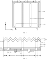
- FIG. 1 is a schematic structural diagram of a solar cell according to an embodiment of the present disclosure.
- FIG. 2 is a cross-sectional view of FIG. 1 along section line A1-A2.
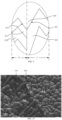
- FIG. 3 is a scanning electron microscope image of a first doped polysilicon layer in a solar cell according to an embodiment of the present disclosure.
- FIG. 4 is a scanning electron microscope image of a second doped polysilicon layer in a solar cell according to an embodiment of the present disclosure.
- the solar cell includes a substrate 100 having a front surface 11 and a rear surface 12 disposed opposite to each other.
- a material of the substrate 100 includes an elemental semiconductor material.
- the elemental semiconductor material is composed of a single element, for example, silicon or germanium.
- the elemental semiconductor material may be in a single crystal state, a polycrystalline state, an amorphous state, or a microcrystalline state (i.e., having the single crystal state and the amorphous state at the same time).
- silicon may be at least one of single crystalline silicon, polysilicon, amorphous silicon, or microcrystalline silicon.
- the material of the substrate 100 includes a compound semiconductor material.
- compound semiconductor materials include, but are not limited to, silicon germanium, silicon carbide, gallium arsenide, indium gallium arsenide, perovskite, cadmium telluride, copper indium selenium and other materials.
- the substrate 100 may also be a sapphire substrate, a silicon substrate on an insulator, or a germanium substrate on the insulator.
- the substrate 100 may be an N-type semiconductor substrate or a P-type semiconductor substrate.
- the N-type semiconductor substrate is doped with an N-type doping element, and the N-type doping element may be any one of group V elements such as phosphorus (P), bismuth (Bi), antimony (Sb), or arsenic (As).
- the P-type semiconductor substrate is doped with a P-type doping element, and the P-type doping element may be any one of group III elements such as boron (B), aluminum (Al), gallium (Ga), or indium (In).
- the front surface 11 is a light receiving surface for receiving incident light
- the rear surface 12 is a backlight surface.
- the solar cell is a double-sided cell, that is, both the front surface and the rear surface of the substrate are light receiving surfaces for receiving incident light.
- the backlight surface is also capable of receiving incident light, but the efficiency of receiving the incident light from the backlight surface is weaker than the efficiency of receiving the incident light from the light receiving surface.
- the substrate 100 has P-type regions and N-type regions spaced from each other and alternatingly arranged.
- the front surface 11 of the substrate 100 has a textured structure 13, and the textured structure 13 includes a regular-shaped pyramid textured structure and an irregular-shaped black silicon.
- An inclined surface of the textured structure can increase internal reflection of incident light, thereby improving the absorption and utilization rate of the substrate on incident light, and further improving the cell efficiency of the solar cell.
- the textured structure 13 includes a plurality of protrusion structures 101, and shapes of the protrusion structures 101 include pyramid shapes, parabolic shapes, or elliptical spherical shapes.
- the front surface 11 of the substrate has a front surface field (FSF) in which doped ions have a conductivity type the same as a conductivity type of doped ions in the substrate, and surface minority concentration is reduced by using the field passivation effect, so that a surface recombination rate is reduced, meanwhile, a series resistance is reduced, and electron transmission capability is improved.
- FSF front surface field
- the rear surface 12 of the substrate is a polishing surface
- the polishing surface refers to a flat surface formed by polishing solution or laser etching to remove the textured structure of the surface. After polishing, flatness of the rear surface is increased, reflection of long-wave light is increased, and secondary absorption of projection light is promoted, thereby improving a short-circuit current. Meanwhile, due to reduction of a specific surface area of the rear surface, recombination on the rear surface is reduced, and the passivation effect of the rear surface is improved.
- the rear surface includes non-electrode regions 2 each provided between a respective one of the P-type regions and a respective one of the N-type regions adjacent to the P-type region, and the passivation layer is formed over the non-electrode regions 2.
- a trench 106 is formed between the P-type region and the N-type region adjacent to each other, so as to achieve automatic isolation between regions of different conductive types, which avoids heavily doped P-type regions and N-type regions of the rear surface of the IBC cell from forming tunnel junctions to cause electric leakage to affect the cell efficiency.
- the solar cell includes first dielectric layers 111 and first doped polysilicon layers 112. Each of the first dielectric layers 111 is formed over a respective one of the N-type regions of the rear surface, and each of the first doped polysilicon layers 112 is formed on a respective one of the first dielectric layers 111 and doped with an N-type doping element.
- a material of a first dielectric layer 111 includes silicon oxide, amorphous silicon, microcrystalline silicon, nanocrystalline silicon, or silicon carbide.
- the first dielectric layer 111 includes a first tunneling dielectric layer, and a passivation contact structure is formed between the first tunneling dielectric layer and the first doped polysilicon layer 112.
- the first doped polysilicon layer 112 is able to form band bending on the surface of the substrate 100, and the first tunneling dielectric layer causes an asymmetric shift of the band on the surface of the substrate 100 such that potential barrier for the majority carriers is lower than potential barrier for the minority carriers, therefore the majority carriers can pass through the first tunneling dielectric layer for quantum tunneling more easily, while the minority carriers have difficulty in passing through the first tunneling dielectric layer, so as to achieve selective transport of carriers.
- the first tunneling dielectric layer has a chemical passivation effect. Specifically, as interface state defects exist at an interface of the substrate 100 and the first tunneling dielectric layer, interface state density of the rear surface of the substrate 100 is large, the increase of the interface state density promotes recombination of photon-generated carriers, and increases the filling factor, the short-circuit current and the open-circuit voltage of the solar cell, so that the photoelectric conversion efficiency of the solar cell is improved.
- the first tunneling dielectric layer is provided on the rear surface 12 of the substrate 100, so that the first tunneling dielectric layer has the chemical passivation effect on the rear surface of the substrate 100. Specifically, the defect state density of the substrate 100 is reduced by saturating dangling bonds of the substrate 100, and the carrier recombination rate is reduced by reducing the recombination center of the substrate 100.
- the first doped polysilicon layer 112 has a field passivation effect. Specifically, an electrostatic field directed to the interior of the substrate 100 is formed on the surface of the substrate 100 to enable minority carriers to escape from the interface, so that concentration of the minority carriers is reduced, the carrier recombination rate at the interface of the substrate 100 is reduced, the open-circuit voltage, the short-circuit current and the filling factor of the solar cell are increased, and the photoelectric conversion efficiency of the solar cell is improved.
- the first doped polysilicon layer 112 is doped with the doping element of the same type as the doping element in the substrate 100, for example, the type of the doping element in the substrate 100 is N-type.
- a concentration of the doping element in the first doped polysilicon layer 112 is greater than a concentration of the doping element in the substrate 100, so as to form a sufficiently high potential barrier on the surface of the substrate 100, so that the majority carriers in the substrate 100 are able to pass through the first tunneling dielectric layer to the first doped polysilicon layer 112.
- the first doped polysilicon layer 112 is doped with the doping element of a conductivity type different from the doping element in the substrate 100.
- the type of the doping element in the substrate 100 is P-type
- the type of the doping element in the first doped polysilicon layer 112 is N-type.
- a PN junction is constructed between the first doped polysilicon layer 112 and the substrate 100, and new hole-electron pairs are formed by the sun shining on the PN junction.
- the photo-generated holes flow to the P-type region under the action of a built-in electric field of the P-N junction, the photo-generated electrons flow to the N-type region, and a current is generated after the circuit is connected.
- a thickness of the first tunneling dielectric layer is in a range of 0.5 nm to 5 nm.
- the thickness of the first tunneling dielectric layer is in a range of 0.5 nm to 1.3 nm, 1.3 nm to 2.6 nm, 2.6 nm to 4.1 nm, or 4.1 nm to 5 nm. If the first tunneling dielectric layer is within any of the above ranges, the thickness of the first tunneling dielectric layer is relatively small, so that the majority carriers can pass through the first tunneling dielectric layer more easily for quantum tunneling, and the minority carriers have difficulty in passing through the first tunneling dielectric layer, so as to realize selective transmission of carriers.
- the first doped polysilicon layer 112 includes a plurality of first silicon grains 1121, and surfaces of the plurality of first silicon grains 1121 form a surface of the first doped polysilicon layer 112 having a first roughness.
- first doped polysilicon layer 112 silicon atoms are arranged in the form of a diamond lattice to form a plurality of crystal nucleuses, the crystal nucleuses grow into grains having crystal planes with different orientations, and the grains are combined to crystallize into polysilicon.
- the first silicon grains refer to grains having crystal planes with different orientations which constitute the polysilicon.
- the first doped polysilicon layer 112 includes the plurality of first silicon grains 1121, surfaces of the plurality of first silicon grains 1121 are uneven so as to construct an uneven surface of the first doped polysilicon layer 112, so the surface of the first doped polysilicon layer 112 has the first roughness.
- a grain size of a first silicon grain1 121 is in a range of 10 nm to 300 nm.
- the grain size of the first silicon grain is in a range of 10 nm to 53 nm, 53 nm to 95.3 nm, 95.3 nm to 138.2 nm, 138.2 nm to 200.6 nm, 200.6 nm to 248 nm, or 248 nm to 300 nm.
- the grain size of the first silicon grain 1121 is within any of the above ranges, so that the roughness of the surface formed by surfaces of the first silicon grains 1121 is large.
- the grain size of the first silicon grain 1121 is within any of the above ranges, the stability between the first silicon grain 1121 and the first silicon grain 1121 is good, and the first doped polysilicon layer 112 is not prone to deformation of the crystal state.
- the stress of the first doped polysilicon layer 112 on the first dielectric layer 111 and a first passivation layer is small, so that film layer performance between the first doped polysilicon layer 112 and the first dielectric layer 111 and between the first doped polysilicon layer 112 and the first passivation layer is improved.
- the shape of the first silicon grain 1121 includes a granular shape. Compared with a block-shaped structure, grain boundaries between granular structures are few, and space between the grain boundaries is large.
- the N-type doping element in the first doped polysilicon layer 112 can migrate through the space between the grain boundaries and is finally collected by the first electrode.
- the granular shape includes a spherical granular shape or a spheroidal granular shape.
- FIG. 3 is a micrograph of a first silicon grain shown by the scanning electrical microscope, and it is seen that the first silicon grain has a granular shape with the same length in three dimensions.
- FIG. 4 is a micrograph of a second silicon grain shown by the scanning electrical microscope, and it is seen that the second silicon grain has a sheet shape extending in two dimensions.
- the solar cell further includes second dielectric layers 121 and second doped polysilicon layers 122.
- Each of the second dielectric layers 121 is formed over a respective one of the P-type regions of the rear surface, and each of the second doped polysilicon layers 122 is formed on a respective one of the second dielectric layers 121.
- the second doped polysilicon layer 122 is doped with a P-type doping element.
- a surface of the first doped polysilicon layer 112 facing away from the substrate 100 has a first roughness
- a surface of the second doped polysilicon layer 122 facing away from the substrate 100 has a second roughness
- the second roughness is less than the first roughness.
- a material of the second dielectric layer 122 includes silicon oxide, amorphous silicon, microcrystalline silicon, nanocrystalline silicon, or silicon carbide.
- the second dielectric layer 121 includes a second tunneling dielectric layer, and a passivation contact structure is formed between the second tunneling dielectric layer and the second doped polysilicon layer 122.
- the second doped polysilicon layer 122 is able to form band bending on the surface of the substrate 100, and the second tunneling dielectric layer causes an asymmetric shift of the band on the surface of the substrate 100 such that potential barrier for the majority carriers is lower than potential barrier for the minority carriers, therefore the majority carriers can pass through the second tunneling dielectric layer for quantum tunneling more easily, while the minority carriers have difficulty in passing through the second tunneling dielectric layer, so as to achieve selective transport of carriers.
- the second tunneling dielectric layer has a chemical passivation effect. Specifically, as interface state defects exist at an interface of the substrate 100 and the second tunneling dielectric layer, interface state density of the rear surface of the substrate 100 is large, the increase of the interface state density promotes recombination of photon-generated carriers, and increases the filling factor, the short-circuit current and the open-circuit voltage of the solar cell, so that the photoelectric conversion efficiency of the solar cell is improved.
- the second tunneling dielectric layer is provided on the rear surface 12 of the substrate 100, so that the second tunneling dielectric layer has the chemical passivation effect on the rear surface of the substrate 100. Specifically, the defect state density of the substrate 100 is reduced by saturating dangling bonds of the substrate 100, and the carrier recombination rate is reduced by reducing the recombination center of the substrate 100.
- the second doped polysilicon layer 122 has a field passivation effect. Specifically, an electrostatic field directed to the interior of the substrate 100 is formed on the surface of the substrate 100 to enable minority carriers to escape from the interface, so that concentration of the minority carriers is reduced, the carrier recombination rate at the interface of the substrate 100 is reduced, the open-circuit voltage, the short-circuit current and the filling factor of the solar cell are increased, and the photoelectric conversion efficiency of the solar cell is improved.
- the second doped polysilicon layer 122 is doped with the doping element of the same type as the doping element in the substrate 100, for example, the type of the doping element in the substrate 100 is P-type.
- a concentration of the doping element in the second doped polysilicon layer 122 is greater than a concentration of the doping element in the substrate 100, so as to form a sufficiently high potential barrier on the surface of the substrate 100, so that the majority carriers in the substrate 100 are able to pass through the second tunneling dielectric layer to the second doped polysilicon layer 122.
- a thickness of the second tunneling dielectric layer is in a range of 0.5 nm to 5 nm.
- the thickness of the second tunneling dielectric layer is in a range of 0.5 nm to 1.3 nm, 1.3 nm to 2.6 nm, 2.6 nm to 4.1 nm, or 4.1 nm to 5 nm. If the second tunneling dielectric layer is within any of the above ranges, the thickness of the second tunneling dielectric layer is relatively small, so that the majority carriers can pass through the second tunneling dielectric layer more easily for quantum tunneling, and the minority carriers have difficulty in passing through the second tunneling dielectric layer, so as to realize selective transmission of carriers.
- the first doped polysilicon layer 112 is doped with the doping element of a conductivity type that is different from a conductivity type of the doping element in the substrate, a PN junction is formed between the first doped polysilicon layer 112 and the substrate, and the first doped polysilicon layer 112 serves as an emitter.
- the second doped polysilicon layer 122 is doped with the doping element of a conductivity type that is different from the conductivity type of the doping element in the substrate, a PN junction is formed between the second doped polysilicon layer 122 and the substrate, and the second doped polysilicon layer 122 serves as the emitter.
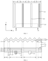
- FIG. 5 is a schematic structural diagram of a solar cell according to an embodiment of the present disclosure
- FIG. 6 is a schematic cross-sectional view of FIG. 5 along section line A1-A2.
- the first dielectric layer 211 includes a first intrinsic dielectric layer, and a heterojunction structure is formed between the first intrinsic dielectric layer and the substrate.
- the first intrinsic dielectric layer has a good passivation effect on the surface of the substrate, recombination of carriers is greatly avoided, and long lifetime of the minority carriers and high open-circuit voltage are achieved.
- the second dielectric layer 221 includes a second intrinsic dielectric layer, and a heterojunction structure is formed between the second intrinsic dielectric layer and the substrate.
- the second intrinsic dielectric layer has a good passivation effect on the surface of the substrate, recombination of carriers is greatly avoided, and long lifetime of the minority carriers and high open-circuit voltage are achieved.
- the materials of the first intrinsic dielectric layer and the second intrinsic dielectric layer include intrinsic amorphous silicon, intrinsic microcrystalline silicon, intrinsic silicon oxide, intrinsic nanocrystalline silicon or intrinsic silicon carbide.
- An optional range of a thickness of the first intrinsic dielectric layer is greater than or equal to 2 microns, less than or equal to 10 microns, and preferably 5 microns.
- An optional range of a thickness of the second intrinsic dielectric layer is greater than or equal to 2 microns, less than or equal to 10 microns, and preferably 5 microns.
- the first intrinsic dielectric layer and the second intrinsic dielectric layer may include a small amount of doping elements, but the intrinsic dielectric layer with a small amount of doping elements is still regarded as a dielectric layer of an intrinsic type.
- a thickness of the first doped polysilicon layer 212 is in a range of 4 nm to 500 nm
- a thickness of the second doped polysilicon layer 222 is in a range of 4 nm to 500 nm.
- the thickness of the second doped polysilicon layer 222 is in a range of 200 nm to 400 nm.
- the thickness of the second doped polysilicon layer 222 is in a range of 20 nm to 103 nm, 103 nm to 139 nm, 139 nm to 161 nm, 161 nm to 218 nm, 218 nm to 298 nm, or 298 nm to 500 nm.
- the solar cell further includes first transparent conductive layers 207 each formed on a surface of a respective one of the first doped polysilicon layers 212 facing away from the substrate, and second transparent conductive layers 202 each formed on a surface of a respective one of the second doped polysilicon layers 222.
- the first electrode 214 is in electrical contact with a first transparent conductive layer 207
- the second electrode 224 is in electrical contact with a second transparent conductive layer 202.
- a material of the first transparent conductive layer 207 includes at least one of indium tin oxide (ITO), aluminum doped zinc oxide (AZO), cerium doped indium oxide, and tungsten doped indium oxide
- a material of the second transparent conductive layer 202 includes at least one of indium tin oxide (ITO), aluminum doped zinc oxide (AZO), cerium doped indium oxide, and tungsten doped indium oxide.
- the first doped polysilicon layer 212 is doped with the doping element of a conductivity type that is different from a conductivity type of the doping element in the substrate 200, a PN junction is formed between the first doped polysilicon layer 212 and the substrate 200, and the first doped polysilicon layer 212 serves as an emitter.
- the second doped polysilicon layer 222 is doped with the doping element of a conductivity type that is different from a conductivity type of the doping element in the substrate, a PN junction is formed between the second doped polysilicon layer 222 and the substrate, and the second doped polysilicon layer 222 serves as the emitter.
- the intrinsic dielectric layer is provided between the PN junction to serve as a buffer layer, and the intrinsic dielectric layer has a good passivation effect on the surface of the substrate 200, so that recombination of carriers is greatly avoided, and relatively long lifetime of the minority carriers and high open-circuit voltage are realized.
- the second doped polysilicon layer 122 includes a plurality of second silicon grains 1221, and surfaces of the plurality of second silicon grains 1221 form a surface of the second doped polysilicon layer 122 having a second roughness.
- a grain size of the first silicon grain 1121 is less than a grain size of the second silicon grain 1221.
- roughness in “first roughness” and “second roughness” refers to an arithmetic mean of absolute values of vertical deviations of a crest and a trough relative to an average horizontal line set in a sampling length.
- the roughness may be measured by comparison measurement, light-sectioning measurement, interference measurement, and stylographic measurement.
- the grain size of the second silicon grain 1221 is in a range of 100 nm to 900 nm.
- the grain size of the second silicon grain 1221 may be in a range of 100 nm to 250 nm, 250 nm to 360 nm, 360 nm to 490 nm, 490 nm to 584 nm, 584 nm to 610 nm, 610 nm to 790 nm, or 790 nm to 900 nm.
- the grain size of the second silicon grain 1221 is within any of the above ranges, a grain boundary between the second silicon grain 1221 and the second silicon grain 1221 is small, and carriers can easily pass through the second doped polysilicon layer 122, thereby improving the carrier migration rate and facilitating the improvement of the cell efficiency.
- the second silicon grain 1221 has a sheet shape, a plate shape, or a granular shape.
- a microstructure of the second silicon grain shown in FIG. 4 is in the sheet shape.
- FIG. 3 and FIG. 4 show surface morphologies of the first doped polysilicon layer 112 and the second doped polysilicon layer 122 at the same magnification, respectively.
- the surface of the first doped polysilicon layer 112 is rougher than the surface of the second doped polysilicon layer 122, that is, the first roughness is greater than the second roughness.
- the surface of the first doped polysilicon layer 112 improves the internal reflection of incident light and reduces the optical loss of the solar cell.
- the first doped polysilicon layer 112 further improves the contact area between the first electrode and the first doped polysilicon layer 112, thereby improving the contact performance and the welding tension of the first doped polysilicon layer 112.
- the surface of the second doped polysilicon layer 122 is smooth, the uniformity of the second passivation layer deposited on the second doped polysilicon layer 122 is good, and the passivation performance of the second passivation layer is good, so that the problem of recombination defects of the solar cell is improved.
- the grain size of the first silicon grain 1121 being less than the grain size of the second silicon grain 1221 includes that a radial one-dimensional size of the first silicon grain 1121 is smaller than a radial one-dimensional size of the second silicon grain, and a height of the first silicon grain 1121 is greater than a height of the second silicon grain 1221. In this way, the roughness of the first doped polysilicon layer 112 formed by the first silicon grains 1121 is greater than the roughness of the second doped polysilicon layer 122 formed by the second silicon grains 1221.
- the radial one-dimensional size of the first silicon grain 1121 refers to a length of an average line (or diameter) of the first silicon grain 1121.
- the height of the first silicon grain 1121 refers to a distance between a side of the first silicon grain 1121 close to the first dielectric layer 111 and a side of the first silicon grain 1121 away from the first dielectric layer 111.
- the radial one-dimensional size of the second silicon grain 1221 refers to a length of an average line (or diameter) of the second silicon grain 1221.
- the height of the second silicon grain 1221 refers to a distance between a side of the second silicon grain 1221 close to the second dielectric layer 121 and a side of the second silicon grain 1221 away from the second dielectric layer 121.
- the first silicon grain 1121 has a granular shape with the same length in three dimensions, and the height of the first silicon grain 1121 is equal to the length of the average line of the first silicon grain 1121.
- the second silicon grain 1221 has the sheet shape extending in two dimensions, and the height of the second silicon grain 1221 is less than the length of the average line of the second silicon grain 1221.
- the height of the second silicon grain 1221 is a length of a line in a direction of a non-extending surface.
- a size of a grain is referred to as the grain size.
- Conventional representations include a number of grains per volume (ZV), a number of grains per unit area (ZS), or a length of an average line (or diameter) of the grain.
- the length of the average line of the grain refers to a length of a line of an extension surface in an extension direction of the grain.
- the grain size in this embodiment of the present disclosure may be the length of the average line of the grain.
- an average thickness of the first doped polysilicon layer 112 is less than or equal to an average thickness of the second doped polysilicon layer 122. In this way, the average thickness of the first doped polysilicon layer 112 is small, and the doping element in the substrate is easily diffused to the first doped polysilicon layer 112, and is then collected by the first electrode.
- the second electrode may burn the second doped polysilicon layer 122 to cause the P-type doping element to be diffused into the substrate due to the fact that the second doped polysilicon layer 122 is too thin.
- the average thickness of the second doped polysilicon layer 122 on the rear surface is large, so that the above risk is reduced, the problem that the P-type doping element in the second doped polysilicon layer 122 is accumulated at the interface of the substrate to form a 'dead layer' is avoided, the carrier transport efficiency is improved, and the generation of the carrier recombination center is reduced.
- the solar cell further includes a passivation layer 123 formed over surfaces of the first doped polysilicon layers 112 facing away from the substrate 100 and surfaces of the second doped polysilicon layers 122 facing away from the substrate 100.
- First electrodes 114 and second electrodes 124 are formed on a surface of the passivation layer 123, the first electrodes 114 are located in the N-type regions and are electrically connected to the first doped polysilicon layers 112, the second electrodes 124 are located in the P-type regions and are electrically connected to the second doped polysilicon layers 122.
- the solar cell further includes a first passivation layer 113, and the first passivation layer 113 is formed over the front surface 11 of the substrate 100.
- the first passivation layer 113 may be a single-layer structure or a laminated structure, and a material of the first passivation layer 113 includes at least one of silicon oxide, silicon nitride, silicon oxynitride, silicon carbonitride oxide, titanium oxide, hafnium oxide, or aluminum oxide, etc.
- the passivation layer 123 may be a single-layer structure or a laminated structure, and a material of the passivation layer 123 includes at least one of silicon oxide, silicon nitride, silicon oxynitride, silicon carbonitride oxide, titanium oxide, hafnium oxide, or aluminum oxide, etc.
- a distance between a first electrode 114 and a second electrode 124 that are adjacent to each other in a first direction X is in a range of 0.5 mm to 2 mm.
- the distance between the first electrode 114 and the second electrode 124 in the first direction X is in a range of 0.5 mm to 0.8 mm, 0.8 mm to 1.15 mm, 1.15 mm to 1.28 mm, 1.28 mm to 1.46 mm, 1.46 mm to 1.68 mm, 1.68 mm to 1.84 mm, or 1.84 mm to 2 mm.
- a width of the first electrode 114 in the first direction X or a width of the second electrode 124 in the first direction X is in a range of 5 ⁇ m to 50 ⁇ m.
- the width of the first electrode 114 in the first direction X or the width of the second electrode 124 in the first direction X is in a range of 5 ⁇ m to 9 ⁇ m, 9 ⁇ m to 14 ⁇ m, 14 ⁇ m to 23 ⁇ m, 23 ⁇ m to 34 ⁇ m, 34 ⁇ m to 42 ⁇ m, 42 ⁇ m to 45 ⁇ m, 45 ⁇ m to 48 ⁇ m, or 48 ⁇ m to 50 ⁇ m.
- the first electrode 114 is sintered from burn-through paste.
- a method for forming the first electrode 114 includes printing metal paste on a surface of a portion of the passivation layer 123 by using a screen-printing process.
- the metal paste includes at least one of silver, aluminum, copper, tin, gold, lead, or nickel.
- a sintering process is performed on the metal paste, and the metal paste has a material of a highly corrosive component such as glass powder, so that the corrosive component corrodes the passivation layer 123 in the sintering process, thereby the metal paste permeates in the passivation layer 123 so as to be in electrical contact with the first doped polysilicon layer 112.
- the second electrode 124 is sintered from burn-through paste.
- the method for forming the second electrode 124 includes printing metal paste on a surface of a portion of the passivation layer 123 by using a screen-printing process.
- the metal paste includes at least one of silver, aluminum, copper, tin, gold, lead, or nickel.
- a sintering process is performed on the metal paste, and the metal paste has a material of a highly corrosive component such as glass powder, so that the corrosive component corrodes the passivation layer 123 in the sintering process, thereby the metal paste permeates in the passivation layer 123 so as to be in electrical contact with the second doped polysilicon layer 122.
- a method for forming a second electrode 224 includes printing metal paste on a surface of a portion of a passivation layer 223 using a screen-printing process.
- the metal paste includes at least one of silver, aluminum, copper, tin, gold, lead, or nickel.
- a sintering process is performed on the metal paste, and the metal paste has a material of a highly corrosive component such as glass powder, so that the corrosive component corrodes the passivation layer 223 in the sintering process, so that the metal paste permeates in the passivation layer 223 so as to be in electrical contact with the second transparent conductive layer 202.
- the substrate is doped with the N-type doping element, and a N-type cell, compared with a P-type cell, has advantages of high conversion rate, low temperature coefficient, high double-sided rate, long lifetime of carriers and the like.
- the first roughness of the first doped polysilicon layer 112 is large, so that the contact performance of the first doped polysilicon layer 112 and the first electrode is good.
- the second roughness of the second doped polysilicon layer 122 is small, so that the film layer performance of the second passivation layer deposited on the second doped polysilicon layer 122 is good, the passivation performance of the second passivation layer is improved, and the cell efficiency is further improved.
- the solar cell includes the first doped polysilicon layers 112 and the second doped polysilicon layers 122 formed over the rear surface, such a fully-passivated contact cell structure greatly reduces the recombination current of the cell, and improves the open-circuit voltage of the cell.
- the process of preparing the fully-passivated contact cell uses the first doped polysilicon layers 112 and the second doped polysilicon layers 122 as the carrier transport layers without the design of the high-temperature diffusion layer, which removes the influence of the recombination current of the diffusion layer, and improves the open-circuit voltage of the cell.
- the first doped polysilicon layers 112 are doped with N-type doping elements, and a surface of a first doped polysilicon layer 112 has a first roughness.
- the second doped polysilicon layers 122 are doped with P-type doping elements, and a surface of a second doped polysilicon layer 122 has a second roughness, and the second roughness is less than the first roughness.
- the first doped polysilicon layer 112 and the second doped polysilicon layer 122 have different morphologies, and for the first doped polysilicon layer 112 with higher roughness, the surface of the first doped polysilicon layer 112 improves the internal reflection of incident light and reduces the optical loss of the solar cell.
- the first doped polysilicon layer 112 further improves the contact area between the first electrode and the first doped polysilicon layer 112, thereby improving the contact performance and the welding tension of the first doped polysilicon layer 112.
- the surface of the second doped polysilicon layer 122 is smooth, the uniformity of the second passivation layer deposited on the second doped polysilicon layer 122 is good, and the passivation performance of the second passivation layer is good, so that the problem of recombination defects of the solar cell is improved.
- the description of the substrate 200, the first passivation layer 213, the first dielectric layers 211, the first doped polysilicon layers 212, an original textured structure 23, the protrusion structures 201, the first electrodes 214, a front surface 21, and a rear surface 22 in FIG. 6 is able to refer to the description of the substrate 100, the first passivation layer 113, the first dielectric layers 111, the first doped polysilicon layers 112, the original textured structure 13, the protrusion structures 101, the first electrodes 114, the front surface 11, and the rear surface 12 in FIG. 2 , which is not repeated herein.
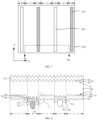
- some embodiments of the present disclosure further provide a solar cell, which differs from the above embodiments in that the rear surface has first surface structures in the P-type regions, each of the second dielectric layers formed on a respective first surface structure, the rear surface has second surface structures in non-electrode regions, and the passivation layer is also formed on the second surface structures.
- a rear surface 32 has a first surface structure 35 in a N-type region and a second surface structure 36 in a non-electrode region 2, a first dielectric layer 311 is formed on the first surface structure 35, and a passivation layer 323 is formed on the second surface structure 34.
- a minimum distance between the first surface structure 35 and a front surface 31 of the substrate is a first minimum distance
- a minimum distance between the second surface structure 34 and the front surface 31 is a second minimum distance
- the first minimum distance is greater than the second minimum distance
- the minimum distance between the first surface structure 35 and the front surface 31 refers to a distance between a portion of the first surface structure closest to the front surface 31 and the front surface 31.
- the minimum distance between the second surface structure 34 and the front surface 31 refers to a distance between a portion of the second surface structure closest to the front surface 31 and the front surface 31.
- the rear surface includes the first surface structures, the second surface structures, and textured structures.
- a difference between the first minimum distance and the second minimum distance is in a range of 0.5 ⁇ m to 10 ⁇ m.
- the difference between the first distance and the second distance is in a range of 0.5 ⁇ m to 2 ⁇ m, 2 ⁇ m to 3.8 ⁇ m, 3.8 ⁇ m to 6.9 ⁇ m, 6.9 ⁇ m to 7.6 ⁇ m, 7.6 ⁇ m to 8.3 ⁇ m, or 8.3 ⁇ m to 10 ⁇ m.
- the first surface structure includes platform protrusion structures, pyramid textured structures, or a flat surface.
- the first surface structure 35 includes a plurality of first protrusion structures 304 arranged at intervals, and in practical application, the arrangement of the plurality of first protrusion structures 304 is not limited. Since the first dielectric layer 311 and the first doped polysilicon layer 312 are thin, the first dielectric layer 311 and the first doped polysilicon layer 312 are able to show morphologies of the first protrusion structures.
- the second surface structure 34 includes a plurality of second protrusion structures 303.
- the arrangement of the plurality of second protrusion structures 303 is not limited.
- At least one of the first surface structure 35 and the second surface structure 34 includes platform protrusion structures or pyramid textured structures.
- the rear surface of the substrate 300 further has third surface structures 36 each located at a junction of the P-type region and the non-electrode region 2 or at a junction of the N-type region and the non-electrode region 2.
- Some of the third surface structures 36 include a first side surface 315 and a second side surface 325.
- the first side surface 315 faces away from the non-electrode region 2, and the first dielectric layer 311 covers the first side surface 315.
- the second side surface 325 faces the non-electrode region 2.
- the first side surface 315 has a radial length that is less than a radial length of the second side surface 325.
- the third surface structure 36 includes prism structures, pyramid structures, or tetrahedral structures.
- the third surface structure 36 has a plurality of third protrusion structures 305 arranged in an intersecting manner, and the third surface structure 36 further has micro-convex structures 345 in addition to the discrete third protrusion structures 305, so that a probability that incident light incident to the junction of the electrode region and the non-electrode region at different angles is reflected at least once and absorbed by the substrate 300 through the third protrusion structures 305 and/or the micro-convex structures 345 is increased, and a probability that the incident light is reflected at least once and reflected by the third protrusion structures 305 and/or the micro-convex structures 345 to the non-electrode region 2 so as to be absorbed by the non-electrode region 2 is increased, thereby improving the absorption rate of the front surface 31 to the incident light.
- the third surface structure 36 includes prism structures, pyramid structures, or tetrahedral structures.
- a micro-convex structure 345 includes at least one of a prism structure inclined toward the N-type region, a second pyramid structure, or a triangular plate-like structure.
- the micro-convex structure 345 includes the prism structure inclined toward the N-type region, the second pyramid structure or the triangular plate-shaped structure as shown in FIG. 11 .
- the micro-convex structure 345 may include only one of the second pyramid structure, the triangular plate-shaped structure, or the prism structure inclined toward the N-type region, or any two of the three.
- the micro-convex structure 345 may be an irregular granular structure in addition to one of the prism structure inclined toward the N-type region, the second pyramid structure, or the triangular plate-shaped structure.
- a one-dimensional size of a bottom of the micro-convex structure 345 includes any one of a length, a width, or a diagonal length of an orthographic projection pattern of the bottom of the micro-convex structure 345 on the substrate 300.
- the orthographic projection pattern of the bottom of the micro-convex structure 345 on the substrate 300 is a regular quadrangle in FIG. 11 .
- the one-dimensional size of the bottom of the micro-convex structure 345 is any one of a length, a width, or a diagonal length of the regular quadrangle.
- the orthographic projection pattern of the bottom of the micro-convex structure 345 on the substrate 300 may also be an irregular polygon, and in this case, the length, width or diagonal length of the orthographic projection pattern of the bottom of the micro-convex structure 345 on the substrate 300 is not absolute, but is artificially defined for representing the one-dimensional size of the bottom of the micro-convex structure 345.
- the orthographic projection pattern of the bottom of the micro-convex structure 345 on the substrate 300 is an irregular quadrangle.
- the length of the orthographic projection pattern of the bottom of the micro-convex structure 345 on the substrate 300 may be defined as a length of the longest edge of the irregular quadrangle
- the width of the orthographic projection pattern of the bottom of the micro-convex structure 345 on the substrate 300 may be defined as a length of the shortest edge of the irregular quadrangle
- the diagonal length of the orthographic projection pattern of the bottom of the micro-convex structure 345 on the substrate 300 may be defined as a length of the longest diagonal of the irregular quadrangle.
- the orthographic projection pattern of the bottom of the micro-convex structure 345 on the substrate 300 may be, in addition to the irregular quadrangle, other irregular polygons, circles, or irregular shapes similar to a circle.
- one-dimensional size of the bottom of the micro-convex structure 345 is measured by selecting a plurality of regions with different specific areas in the bottom of the micro-convex structure 345 and obtaining an average value of lengths, widths, diagonal lengths or diameters of the regions with the different specific areas, where the regions with the specific areas are flexibly defined according to actual requirements.
- the orthographic projection pattern of the bottom of the third protrusion structure 305 on the substrate 300 is generally a regular quadrangle, and in this case, one-dimensional size of the bottom of the third protrusion structure 305 is any one of a length, a width, or a diagonal length of the regular quadrangle.
- the orthographic projection pattern of the bottom of the third protrusion structure 305 on the substrate 300 may be an irregular quadrangle, and the definition of one-dimensional size of the bottom of the third protrusion structure 305 in this case is similar to the definition of one-dimensional size of the orthographic projection pattern of the bottom of the micro-convex structure 345 on the substrate 300 when it is the irregular quadrangle, which is not repeated herein.
- one-dimensional sizes of bottoms of different third protrusion structures 305 may be different or the same, but the one-dimensional sizes of the bottoms of the third protrusion structures 305 are within a numerical range.
- One-dimensional sizes of bottoms of different micro-convex structures 345 may be different or the same, but the one-dimensional sizes of the bottoms of the third protrusion structures 305 are also within a numerical range.
- the one-dimensional size of the bottom of the micro-convex structure 345 being smaller than that of the bottom of the third protrusion structure 305 means that an average value of the one-dimensional sizes of the bottoms of the plurality of micro-convex structures 345 is smaller than an average value of the one-dimensional sizes of the bottoms of the plurality of third protrusion structures 305.
- the prism structures are located on side surfaces of the third protrusion structures 305.
- the following two arrangements of the prism structures on the side surfaces of the third protrusion structures 305 are provided.
- one prism structure is located on a side surface of one third protrusion structure 305.
- a plurality of prism structures are attached to the same side surface of one third protrusion structure 305, and each prism structure is in contact and connection with the side surface.
- some of the prism structures are located at a portion of the junction adjacent to the N-type region.
- the prism structures are located between the third protrusion structures 305 and the N-type region.
- the plurality of prism structures are sequentially arranged in a direction away from the side surface of the third protrusion structure 305. For example, only the prism structure closest to the side surface of the third protrusion structure 305 among the plurality of prism structures is in contact and connection with the side surface of the third protrusion structure 305.
- the plurality of prism structures at the same junction include at least one of the prism structures described in the above three kind of embodiments, that is, the plurality of prism structures at the same junction may have the characteristics of the prism structures in the above three kind of embodiments, or have the characteristics of the prism structures in any two of the above three kind of embodiments, or have the characteristics of the prism structures in any one of the above three kind of embodiments.
- a bottom of the second pyramid structure is in contact and connection with the bottom of the third protrusion structure 305.
- a periphery of the bottom of one third protrusion structure 305 is surrounded with a plurality of second pyramid structures, and the bottom of each second pyramid structure is in contact and connection with the bottom of the third protrusion structure 305.
- At least one second pyramid structure is located at the interval between two adjacent third protrusion structures 305. In other words, the bottom of the second pyramid structure is not in contact and connection with the bottom of the third protrusion structure 305.
- the second pyramid structures at the same junction include the second pyramid structures in at least one of the above two kind of embodiments, that is, the plurality of second pyramid structures at the same junction may have the characteristics of the second pyramid structures in the above two kind of embodiments, or have the characteristics of the second pyramid structures in any one of the above two kind of embodiments.
- one triangular plate-like structure is located on a side surface of one third protrusion structure 305 in some cases, and in other cases, a plurality of triangular plate-like structures are attached to the same side surface of one third protrusion structure 305, and each triangular plate-like structure is in contact and connection with the side surface.
- the plurality of triangular plate-like structures are sequentially arranged in a direction away from the side surface of the third protrusion structure 305. For example, only the triangular plate-like structure closest to the side surface of the third protrusion structure 305 among the plurality of triangular plate-like structures is in contact and connection with the side surface of the third protrusion structure 305.
- the triangular plate-like structures at the same junction include the triangular plate-like structures in at least one of the above two kind of embodiments, that is, the plurality of triangular plate-like structures at the same junction may have the characteristics of the triangular plate-like structures in the above two kind of embodiments, or have the characteristics of the triangular plate-like structures in any one of the above two kind of embodiments.
- the third protrusion structure 305 is located at a portion of the junction adjacent to the non-electrode region 2. In other words, there are more typical third protrusion structures 305 at the portion of the junction adjacent to the non-electrode region 2.
- the third surface structures 36 at the junction are described in various embodiments, i.e., the structure of the third surface structure 36 has diversity.
- the plurality of micro-convex structures 345 are also provided at the same junction at which the third protrusion structures 305 are provided, and the specific characteristics of the plurality of micro-convex structures 345 at different junctions may be different.
- one of two adjacent junctions has the prism structures inclined toward the N-type region and the second pyramid structures, and the other has the second pyramid structures and the triangular plate-like structures.
- the third surface structure 36 further includes first prism structures 335, a first length of a third protrusion structure 305 is greater than a second length of a first prism structure 335 in an inclined direction of the first prism structure 335, and at least some of the first prism structures 335 are located on side surfaces of the third protrusion structures 305 away from the N-type region. In this way, the probability that the incident light incident to the junction is absorbed by the junction or the non-electrode region 2 is further improved.
- an inclined length of the shortest one of the plurality of third protrusion structures 305 is defined as the first length of the third protrusion structure 305
- an inclined length of the longest one of the plurality of first prism structures 335 is defined as the second length of the first prism structure 335.
- the first length of the third protrusion structure 305 being greater than the second length of the first prism structure 335 refers to that the inclined length of the shortest one of the plurality of third protrusion structures 305 is greater than the inclined length of the longest one of the plurality of first prism structures 335.
- an average value of inclined lengths of the plurality of third protrusion structures 305 is defined as the first length of the third protrusion structure 305
- an average value of inclined lengths of the plurality of first prism structures 335 is defined as the second length of the first prism structure 335.
- the first length of the third protrusion structure 305 being greater than the second length of the first prism structure 335 refers to that the average value of the inclined lengths of the plurality of third protrusion structures 305 is greater than the average value of the inclined lengths of the plurality of first prism structures 335.
- two arrangements of the second prism structures 335 on the side surfaces of the third protrusion structures 305 away from the N-type region are provided.
- one second prism structure 335 is located on a side surface of one third protrusion structure 305 away from the N-type region.
- the plurality of first prism structures 335 are located on a side surface of one second prism structure 335 away from the N-type region, and each first prism structure 335 is in contact and connection with the side surface.
- the plurality of first prism structures 335 are sequentially arranged in a direction away from the side surface of the third protrusion structure 305. For example, only the first prism structure 335 closest to the side surface of the third protrusion structure 305 among the plurality of first prism structures 335 is in contact and connection with the side surface of the third protrusion structure 305.
- the third surface structure 36 further includes first pyramid structures, and at least some of the first pyramid structures are located on a portion of the junction.
- a one-dimensional size of a bottom of the third protrusion structure is greater than a one-dimensional size of a bottom of the first protrusion structure, and the one-dimensional size of the bottom of the first protrusion structure is greater than a one-dimensional size of a bottom of the second protrusion structure.
- one-dimensional sizes of bottoms of different first protrusion structures may be different or the same, but the one-dimensional sizes of the bottoms of the first protrusion structures are within a numerical range.
- One-dimensional sizes of bottoms of different second protrusion structures may be different or the same, but the one-dimensional sizes of the bottoms of the second protrusion structures are also within a numerical range.
- the one-dimensional size of the bottom of the third protrusion structure being greater than that of the bottom of the first protrusion structure refers to that an average value of the one-dimensional sizes of the bottoms of the plurality of third protrusion structures is greater than an average value of the one-dimensional sizes of the bottoms of the first protrusion structures
- the one-dimensional size of the bottom of the first protrusion structure is greater than that of the bottom of the second protrusion structure refers to that an average value of the one-dimensional sizes of the bottoms of the plurality of first protrusion structures on which the first doped polysilicon layers are formed is greater than an average value of the one-dimensional sizes of the bottoms of the plurality of second protrusion structures in the non-electrode regions 2.
- a size relationship between the one-dimensional size of the bottom of the second protrusion structure and the one-dimensional size of the bottom of the second protrusion structure is not limited in the embodiments of the present disclosure.
- some embodiments of the present disclosure further provide a method for preparing a solar cell, which may be used to prepare the solar cell provided in the above embodiments, and technical features the same as or corresponding to the technical features in the above embodiments are not repeated herein.
- the method for preparing the solar cell shown in FIG. 8 is taken as an example.
- the method includes providing an initial substrate having a first surface and a second surface opposite to each other, and the initial substrate is doped with an N-type doping element or a P-type doping element.
- polishing treatment is performed on two opposite surfaces of the initial substrate, and the polishing treatment is used to reduce surface defects of the substrate.
- the initial substrate has first regions and second regions that are spaced from each other and alternatingly arranged as well as initial non-electrode regions each provided between a first region and a second region adjacent to each other.
- the method includes performing texturing treatment on the second surface of the initial substrate, so that the second surface of the initial substrate forms a textured structure.
- the texturing treatment includes chemical etching, for example, a mixed solution of potassium hydroxide and hydrogen peroxide may be used to clean the initial substrate, and specifically, the textured structure conforming to the expectation can be formed by controlling a ratio of concentration of the potassium hydroxide solution to concentration of the hydrogen peroxide solution.
- the textured structure may also be formed by methods such as laser etching, mechanical or plasma etching. In the laser etching, the textured structure conforming to the expectation is obtained by controlling laser process parameters.
- the method includes forming a first initial dielectric layer and a first semiconductor layer stacked on the first surface.
- the first initial dielectric layer is formed in the first regions, the second regions and the initial non-electrode regions, and the first semiconductor layer is formed on a surface of the first initial dielectric layer facing away from the initial substrate.
- a surface of the first semiconductor layer facing away from the first initial dielectric layer has a first initial roughness.
- the first semiconductor layer is patterned, portions of the first initial dielectric layer in the first regions are reserved as first dielectric layers, portions of the first semiconductor layer in the first regions are reserved as first doped polysilicon layers, and a surface of a first doped polysilicon layer facing away from the initial substrate has a first roughness.
- the first regions, second regions and initial non-electrode regions are respectively N-type regions, P-type regions and non-electrode regions
- the initial substrate is a substrate, the first surface of the initial substrate serves as a rear surface, and the second surface of the initial substrate serves as a front surface.
- Some of the third surface structures include a first side surface and a second side surface, the first side surface faces away from the non-electrode region, and the second side surface faces the non-electrode region.
- a radial length of the first side surface is less than a radial length of the second side surface.
- the first surface structures are prepared with the textured structures in the same preparation process, that is, both the first surface and the second surface of the initial substrate are textured.
- the method includes forming second dielectric layers and second doped polysilicon layers over the rear surface.
- Each second dielectric layer is formed in a second region and on a surface of a second dielectric layer facing away from the substrate, and a surface of the second doped polysilicon layer facing away from the substrate has a second roughness.
- the second roughness is less than the first roughness.
- the first semiconductor layer and the second doped polysilicon layers may be crystallized simultaneously, and in this process, a surface of the first semiconductor layer facing away from the substrate has a first roughness, and a surface of the second doped polysilicon layer facing away from the substrate has a second roughness.
- the crystallization process includes annealing or laser activation.
- the method before performing the patterning process, further includes forming mask layers on portions of the surface of the first semiconductor layer in the first regions, so as to reduce etching damage to the first doped polysilicon layers in the patterning process.
- a material of the mask layer includes organic wax, metal, or a silicon dioxide mask.
- the mask layer is formed by using a printing process.
- the mask layer may be removed by using an etching process, and the etching process includes any one of a dry etching process, a wet etching process, or a laser etching process.
- the patterning process includes a wet etching process or a laser etching process.
- the process parameters of the wet etching process include a reaction solution including an acid solution, and a reaction time in a range of 50 s to 550 s.
- the steps of the wet etching process include (1) using a mixed acid solution containing HF, HNO 3 , H 2 SO 4 , with mass concentration of 10% to 25%, 5% to 10%, and 2% to 4%, respectively, patterning the surface in the non-metal regions using the mixed acid solution in a screen printing manner with an amount of 0.05 mL/cm 2 to 0.8 mL/cm 2 and a time for 50 s to 550 s; (2) using deionized water/low-concentration alkali solution (0.5% to 1% NaOH)/low-concentration HCl (2.5% to 3.5%) for alternate cleaning for 2 times after the patterning.
- the method includes forming a passivation layer over surfaces of the first doped polysilicon layers and surfaces of the second doped polysilicon layers, and the passivation layer is further formed over the non-electrode regions.
- the method includes forming first electrodes and second electrodes on the surface of the passivation layer facing away from the substrate, the first electrodes are located in the N-type regions and electrically connected to the first doped polysilicon layers, and the second electrodes are located in the P-type regions and electrically connected to the second doped polysilicon layers.
- FIG. 12 is a schematic structural diagram of a photovoltaic module according to an embodiment of the present disclosure.
- FIG. 13 is a cross-sectional view of FIG. 12 along section line M1-M2.
- some embodiments of the present disclosure provide a photovoltaic module including the solar cell in the above embodiments, and the same parts as those in the above embodiments are not repeated herein.
- the photovoltaic module includes at least one cell string each formed by connecting a plurality of solar cells 40 according to any one of the above embodiments or a plurality of solar cells prepared by the method according to any one of the above embodiments through at least one connecting member 409, at least one encapsulation layer 47 each configured to cover a surface of a respective cell string, and at least one cover plate 48 each configured to cover a surface of a respective encapsulation layer 47 facing away from the cell string.
- the plurality of solar cells are electrically connected by means of the at least one connecting member 409, and the connecting members 409 are welded to busbars 408 on the solar cells.
- a gap is not provided between the solar cells, that is, the solar cells overlap with each other.
- the at least one connection member is welded to finger electrodes on the solar cells, and the finger electrodes include first electrodes 414 and second electrodes 424.
- the at least one encapsulation layer includes a first encapsulation layer and a second encapsulation layer, the first encapsulation layer covers one of the front surface or the rear surface of the solar cell, and the second encapsulation layer covers the other of the front surface or the rear surface of the solar cell.
- at least one of the first encapsulation layer or the second encapsulation layer may be an organic encapsulation adhesive film such as polyvinyl butyral (PVB) adhesive film, ethylene-vinyl acetate copolymer (EVA) adhesive film, polyethylene octene co-elastomer (POE) adhesive film or polyethylene terephthalate (PET) adhesive film.
- PVB polyvinyl butyral
- EVA ethylene-vinyl acetate copolymer
- POE polyethylene octene co-elastomer
- PET polyethylene terephthalate
- first encapsulation layer and the second encapsulation layer have a boundary before lamination processing, and the photovoltaic module formed after the lamination processing does not have the so-called first encapsulation layer and second encapsulation layer, that is, the first encapsulation layer and the second encapsulation layer have formed an integral encapsulation layer 47.
- the at least one cover plate 48 may be a cover plate having a light-transmitting function, such as a glass cover plate and a plastic cover plate. Specifically, a surface of the cover plate 48 facing the encapsulation layer 47 may be a concave-convex surface, thereby increasing the utilization rate of incident light.
- the at least one cover plate 48 includes a first cover plate and a second cover plate, the first cover plate faces the first encapsulation layer and the second cover plate faces the second encapsulation layer, or, the first cover plate faces one side of the solar cell and the second cover plate faces the other side of the solar cell.
Landscapes
- Photovoltaic Devices (AREA)
- Life Sciences & Earth Sciences (AREA)
- Sustainable Development (AREA)
- Chemical & Material Sciences (AREA)
- Crystallography & Structural Chemistry (AREA)
Applications Claiming Priority (1)
| Application Number | Priority Date | Filing Date | Title |
|---|---|---|---|
| CN202311736451.7A CN118053927A (zh) | 2023-12-15 | 2023-12-15 | 太阳能电池及其制备方法、光伏组件 |
Publications (1)
| Publication Number | Publication Date |
|---|---|
| EP4571845A1 true EP4571845A1 (fr) | 2025-06-18 |
Family
ID=89715943
Family Applications (1)
| Application Number | Title | Priority Date | Filing Date |
|---|---|---|---|
| EP24153724.0A Pending EP4571845A1 (fr) | 2023-12-15 | 2024-01-24 | Cellule solaire, son procédé de préparation et module photovoltaïque |
Country Status (4)
| Country | Link |
|---|---|
| US (1) | US12166142B1 (fr) |
| EP (1) | EP4571845A1 (fr) |
| JP (1) | JP7527510B1 (fr) |
| CN (1) | CN118053927A (fr) |
Families Citing this family (8)
| Publication number | Priority date | Publication date | Assignee | Title |
|---|---|---|---|---|
| CN118380482B (zh) * | 2024-06-24 | 2024-09-27 | 浙江爱旭太阳能科技有限公司 | 一种背接触太阳能电池、电池组件及光伏系统 |
| CN118943223A (zh) * | 2024-07-24 | 2024-11-12 | 浙江爱旭太阳能科技有限公司 | 一种太阳能电池、电池组件及光伏系统 |
| CN119008716A (zh) * | 2024-08-09 | 2024-11-22 | 珠海富山爱旭太阳能科技有限公司 | 一种太阳能电池及其钝化接触结构、电池组件及光伏系统 |
| CN118888619A (zh) * | 2024-09-06 | 2024-11-01 | 浙江爱旭太阳能科技有限公司 | 一种太阳能电池、电池组件及光伏系统 |
| WO2026056252A1 (fr) * | 2024-09-13 | 2026-03-19 | 西安隆基乐叶光伏科技有限公司 | Cellule solaire et module photovoltaïque |
| CN120076483B (zh) * | 2025-01-24 | 2026-01-30 | 西安隆基乐叶光伏科技有限公司 | 一种背接触电池和光伏组件 |
| CN120957525A (zh) * | 2025-10-15 | 2025-11-14 | 浙江爱旭太阳能科技有限公司 | 背接触电池片、光伏组件和光伏系统 |
| CN121358053B (zh) * | 2025-12-17 | 2026-04-24 | 浙江晶科能源有限公司 | 太阳能电池、其制备方法、叠层电池和光伏组件 |
Citations (3)
| Publication number | Priority date | Publication date | Assignee | Title |
|---|---|---|---|---|
| US9525083B2 (en) * | 2015-03-27 | 2016-12-20 | Sunpower Corporation | Solar cell emitter region fabrication with differentiated P-type and N-type architectures and incorporating a multi-purpose passivation and contact layer |
| US20190267499A1 (en) * | 2016-04-01 | 2019-08-29 | Sunpower Corporation | Metallization of solar cells with differentiated p-type and n-type region architectures |
| CN115566088A (zh) * | 2022-08-22 | 2023-01-03 | 泰州隆基乐叶光伏科技有限公司 | 一种背接触电池及其制造方法、光伏组件 |
Family Cites Families (51)
| Publication number | Priority date | Publication date | Assignee | Title |
|---|---|---|---|---|
| US6114046A (en) | 1997-07-24 | 2000-09-05 | Evergreen Solar, Inc. | Encapsulant material for solar cell module and laminated glass applications |
| JP2005142268A (ja) | 2003-11-05 | 2005-06-02 | Canon Inc | 光起電力素子およびその製造方法 |
| US8222516B2 (en) | 2008-02-20 | 2012-07-17 | Sunpower Corporation | Front contact solar cell with formed emitter |
| US7851698B2 (en) | 2008-06-12 | 2010-12-14 | Sunpower Corporation | Trench process and structure for backside contact solar cells with polysilicon doped regions |
| JPWO2013015173A1 (ja) | 2011-07-25 | 2015-02-23 | 日立化成株式会社 | 太陽電池基板、太陽電池基板の製造方法、太陽電池素子及び太陽電池 |
| US20130130508A1 (en) | 2011-09-02 | 2013-05-23 | Air Products And Chemicals, Inc. | Compositions and Methods for Texturing of Silicon Wafers |
| CN104170095B (zh) | 2012-03-14 | 2016-10-19 | Imec非营利协会 | 用于制造具有镀敷触点的光伏电池的方法 |
| US9054255B2 (en) | 2012-03-23 | 2015-06-09 | Sunpower Corporation | Solar cell having an emitter region with wide bandgap semiconductor material |
| US20130295712A1 (en) | 2012-05-03 | 2013-11-07 | Advanced Technology Materials, Inc. | Methods of texturing surfaces for controlled reflection |
| CN109599450A (zh) | 2013-04-03 | 2019-04-09 | Lg电子株式会社 | 太阳能电池 |
| KR20140146998A (ko) | 2013-06-17 | 2014-12-29 | 전영권 | 태양전지 및 그 제조방법 |
| JP2015082512A (ja) | 2013-10-21 | 2015-04-27 | 株式会社日立ハイテクノロジーズ | 太陽電池の製造方法、太陽電池およびバスバー電極形成用導電性ペースト |
| JP2015185587A (ja) * | 2014-03-20 | 2015-10-22 | シャープ株式会社 | 光電変換素子および光電変換素子の製造方法 |
| US20150349180A1 (en) | 2014-05-30 | 2015-12-03 | David D. Smith | Relative dopant concentration levels in solar cells |
| KR101569415B1 (ko) | 2014-06-09 | 2015-11-16 | 엘지전자 주식회사 | 태양 전지의 제조 방법 |
| JP6176195B2 (ja) | 2014-06-30 | 2017-08-09 | 信越化学工業株式会社 | 太陽電池 |
| CN106575676B (zh) | 2014-07-17 | 2019-06-28 | 光城公司 | 具有叉指背接触的太阳能电池 |
| US10546172B2 (en) | 2015-03-30 | 2020-01-28 | Temptime Corporation | Two dimensional barcode with dynamic environmental data system, method, and apparatus |
| KR102373649B1 (ko) | 2015-05-28 | 2022-03-11 | 엘지전자 주식회사 | 태양 전지 및 이의 제조 방법 |
| KR101740523B1 (ko) | 2015-12-21 | 2017-05-26 | 엘지전자 주식회사 | 태양 전지 및 그 제조 방법 |
| KR101751946B1 (ko) | 2015-12-28 | 2017-06-28 | 엘지전자 주식회사 | 태양 전지 모듈 |
| KR102526398B1 (ko) | 2016-01-12 | 2023-04-27 | 상라오 징코 솔라 테크놀러지 디벨롭먼트 컴퍼니, 리미티드 | 태양 전지 및 이의 제조 방법 |
| EP3435426B1 (fr) | 2016-03-23 | 2020-07-01 | Panasonic Intellectual Property Management Co., Ltd. | Cellule solaire, module de cellule solaire et procédé de fabrication de cellule solaire |
| NL2017872B1 (en) | 2016-11-25 | 2018-06-08 | Stichting Energieonderzoek Centrum Nederland | Photovoltaic cell with passivating contact |
| EP3358627B1 (fr) | 2017-02-07 | 2024-11-13 | Shangrao Xinyuan YueDong Technology Development Co. Ltd | Cellule solaire |
| CN206595264U (zh) | 2017-03-10 | 2017-10-27 | 泰州隆基乐叶光伏科技有限公司 | 一种钝化接触全背电极太阳电池结构 |
| KR20180119969A (ko) | 2017-04-26 | 2018-11-05 | 엘지전자 주식회사 | 태양 전지 및 이의 제조 방법 |
| KR101930640B1 (ko) | 2017-08-08 | 2018-12-18 | 아주대학교산학협력단 | 저반사 구조물과 이의 제조방법, 이를 포함하는 태양전지 및 광학 필름 |
| GB201721066D0 (en) | 2017-12-15 | 2018-01-31 | Oxford Photovoltaics Ltd | Multi-function photovoltaic device |
| CN108336154A (zh) | 2018-02-02 | 2018-07-27 | 中国科学院微电子研究所 | 晶体硅太阳能电池及其制备方法 |
| WO2019163646A1 (fr) | 2018-02-23 | 2019-08-29 | 株式会社カネカ | Procédé de production de cellule solaire |
| JP7126909B2 (ja) | 2018-09-12 | 2022-08-29 | 東洋アルミニウム株式会社 | バックコンタクト型太陽電池セルの製造方法 |
| CN109256440A (zh) | 2018-09-17 | 2019-01-22 | 浙江爱旭太阳能科技有限公司 | 一种选择性钝化接触晶体硅太阳能电池及其制备方法 |
| KR102102823B1 (ko) | 2018-10-30 | 2020-04-22 | 성균관대학교산학협력단 | 표면 구조를 이용한 선택적 에미터의 형성 방법 및 표면 구조를 이용한 선택적 에미터를 포함한 태양전지 |
| KR20210010095A (ko) | 2019-07-19 | 2021-01-27 | 엘지전자 주식회사 | 태양 전지 및 이의 제조 방법 |
| CN110676160A (zh) | 2019-10-10 | 2020-01-10 | 浙江晶科能源有限公司 | 一种太阳能电池及其制作方法 |
| CN111755552A (zh) | 2020-07-20 | 2020-10-09 | 晶科能源有限公司 | 太阳能电池及其制作方法 |
| CN111739984A (zh) | 2020-08-10 | 2020-10-02 | 浙江晶科能源有限公司 | 太阳能电池及其制作方法 |
| CN112201701B (zh) | 2020-09-30 | 2024-05-03 | 浙江晶科能源有限公司 | 太阳能电池和光伏组件 |
| CN114388639B (zh) | 2020-10-21 | 2026-03-10 | 福建新峰二维材料科技有限公司 | 一种铸锭晶硅异质结太阳能电池及其制作方法 |
| CN113327999B (zh) | 2021-06-17 | 2023-04-07 | 中国科学院上海微系统与信息技术研究所 | 表面具有凹槽的单晶硅片、异质结太阳电池及制备方法 |
| JP7168800B1 (ja) | 2021-12-09 | 2022-11-09 | ジョジアン ジンコ ソーラー カンパニー リミテッド | 太陽電池及び光起電力モジュール |
| CN116722056A (zh) | 2022-05-26 | 2023-09-08 | 浙江晶科能源有限公司 | 太阳能电池及太阳能电池的制备方法、光伏组件 |
| CN116741849A (zh) | 2022-06-08 | 2023-09-12 | 浙江晶科能源有限公司 | 一种太阳能电池及光伏组件 |
| CN116741850A (zh) | 2022-06-08 | 2023-09-12 | 浙江晶科能源有限公司 | 一种太阳能电池及光伏组件 |
| CN114784148B (zh) | 2022-06-15 | 2022-09-23 | 浙江晶科能源有限公司 | 太阳能电池的制备方法及太阳能电池、光伏组件 |
| CN116936658A (zh) | 2022-06-21 | 2023-10-24 | 浙江晶科能源有限公司 | 背接触太阳能电池及光伏组件 |
| CN218975458U (zh) | 2022-08-22 | 2023-05-05 | 泰州隆基乐叶光伏科技有限公司 | 一种背接触电池 |
| CN117712199A (zh) | 2022-09-08 | 2024-03-15 | 浙江晶科能源有限公司 | 太阳能电池及光伏组件 |
| CN218585994U (zh) | 2022-09-08 | 2023-03-07 | 浙江晶科能源有限公司 | 太阳能电池及光伏组件 |
| CN116632093A (zh) | 2023-04-21 | 2023-08-22 | 晶科能源(海宁)有限公司 | 太阳能电池及其制备方法、光伏组件 |
-
2023
- 2023-12-15 CN CN202311736451.7A patent/CN118053927A/zh active Pending
-
2024
- 2024-01-24 EP EP24153724.0A patent/EP4571845A1/fr active Pending
- 2024-01-26 US US18/424,563 patent/US12166142B1/en active Active
- 2024-01-30 JP JP2024011874A patent/JP7527510B1/ja active Active
Patent Citations (3)
| Publication number | Priority date | Publication date | Assignee | Title |
|---|---|---|---|---|
| US9525083B2 (en) * | 2015-03-27 | 2016-12-20 | Sunpower Corporation | Solar cell emitter region fabrication with differentiated P-type and N-type architectures and incorporating a multi-purpose passivation and contact layer |
| US20190267499A1 (en) * | 2016-04-01 | 2019-08-29 | Sunpower Corporation | Metallization of solar cells with differentiated p-type and n-type region architectures |
| CN115566088A (zh) * | 2022-08-22 | 2023-01-03 | 泰州隆基乐叶光伏科技有限公司 | 一种背接触电池及其制造方法、光伏组件 |
Also Published As
| Publication number | Publication date |
|---|---|
| CN118053927A (zh) | 2024-05-17 |
| US12166142B1 (en) | 2024-12-10 |
| JP2025096093A (ja) | 2025-06-26 |
| JP7527510B1 (ja) | 2024-08-02 |
Similar Documents
| Publication | Publication Date | Title |
|---|---|---|
| US12166142B1 (en) | Solar cell, method for preparing the same, and photovoltaic module | |
| US12278303B1 (en) | Solar cell and photovoltaic module | |
| JP7618868B1 (ja) | 太陽電池及びその製造方法、光起電力モジュール | |
| JP7639208B1 (ja) | 太陽電池及びその製造方法、積層電池、並びに光起電力モジュール | |
| JP7814575B2 (ja) | 太陽電池及び光起電力モジュール | |
| JP7644287B1 (ja) | 太陽電池及び光起電力モジュール | |
| EP4629787A1 (fr) | Cellule solaire | |
| US20250338668A1 (en) | Solar cell and photovoltaic module | |
| US12543403B2 (en) | Solar cell, method for preparing solar cell, and photovoltaic module | |
| CN118053922A (zh) | 太阳能电池及其制备方法、光伏组件 | |
| CN118335814A (zh) | 背接触太阳能电池、光伏组件 | |
| US20250098365A1 (en) | Solar cell, method for preparing the same, and photovoltaic module | |
| CN220934090U (zh) | 太阳能电池及光伏组件 | |
| CN118053921A (zh) | 太阳能电池及其制备方法、光伏组件 | |
| US12278295B1 (en) | Solar cell, method for manufacturing solar cell, and photovoltaic module | |
| US12376415B2 (en) | Solar cell and photovoltaic module |
Legal Events
| Date | Code | Title | Description |
|---|---|---|---|
| PUAI | Public reference made under article 153(3) epc to a published international application that has entered the european phase |
Free format text: ORIGINAL CODE: 0009012 |
|
| STAA | Information on the status of an ep patent application or granted ep patent |
Free format text: STATUS: REQUEST FOR EXAMINATION WAS MADE |
|
| 17P | Request for examination filed |
Effective date: 20240124 |
|
| AK | Designated contracting states |
Kind code of ref document: A1 Designated state(s): AL AT BE BG CH CY CZ DE DK EE ES FI FR GB GR HR HU IE IS IT LI LT LU LV MC ME MK MT NL NO PL PT RO RS SE SI SK SM TR |
|
| STAA | Information on the status of an ep patent application or granted ep patent |
Free format text: STATUS: EXAMINATION IS IN PROGRESS |
|
| 17Q | First examination report despatched |
Effective date: 20260216 |