EP4574424A1 - Bande de découpage en dés et procédés associés - Google Patents
Bande de découpage en dés et procédés associés Download PDFInfo
- Publication number
- EP4574424A1 EP4574424A1 EP23219993.5A EP23219993A EP4574424A1 EP 4574424 A1 EP4574424 A1 EP 4574424A1 EP 23219993 A EP23219993 A EP 23219993A EP 4574424 A1 EP4574424 A1 EP 4574424A1
- Authority
- EP
- European Patent Office
- Prior art keywords
- dicing tape
- outer layer
- layer
- dicing
- base layer
- Prior art date
- Legal status (The legal status is an assumption and is not a legal conclusion. Google has not performed a legal analysis and makes no representation as to the accuracy of the status listed.)
- Pending
Links
Images

Classifications
-
- H—ELECTRICITY
- H10—SEMICONDUCTOR DEVICES; ELECTRIC SOLID-STATE DEVICES NOT OTHERWISE PROVIDED FOR
- H10P—GENERIC PROCESSES OR APPARATUS FOR THE MANUFACTURE OR TREATMENT OF DEVICES COVERED BY CLASS H10
- H10P72/00—Handling or holding of wafers, substrates or devices during manufacture or treatment thereof
- H10P72/70—Handling or holding of wafers, substrates or devices during manufacture or treatment thereof for supporting or gripping
- H10P72/74—Handling or holding of wafers, substrates or devices during manufacture or treatment thereof for supporting or gripping using temporarily an auxiliary support
- H10P72/7402—Wafer tapes, e.g. grinding or dicing support tapes
-
- B—PERFORMING OPERATIONS; TRANSPORTING
- B32—LAYERED PRODUCTS
- B32B—LAYERED PRODUCTS, i.e. PRODUCTS BUILT-UP OF STRATA OF FLAT OR NON-FLAT, e.g. CELLULAR OR HONEYCOMB, FORM
- B32B27/00—Layered products comprising a layer of synthetic resin
- B32B27/06—Layered products comprising a layer of synthetic resin as the main or only constituent of a layer, which is next to another layer of the same or of a different material
- B32B27/08—Layered products comprising a layer of synthetic resin as the main or only constituent of a layer, which is next to another layer of the same or of a different material of synthetic resin
-
- B—PERFORMING OPERATIONS; TRANSPORTING
- B32—LAYERED PRODUCTS
- B32B—LAYERED PRODUCTS, i.e. PRODUCTS BUILT-UP OF STRATA OF FLAT OR NON-FLAT, e.g. CELLULAR OR HONEYCOMB, FORM
- B32B27/00—Layered products comprising a layer of synthetic resin
- B32B27/18—Layered products comprising a layer of synthetic resin characterised by the use of special additives
- B32B27/20—Layered products comprising a layer of synthetic resin characterised by the use of special additives using fillers, pigments, thixotroping agents
-
- B—PERFORMING OPERATIONS; TRANSPORTING
- B32—LAYERED PRODUCTS
- B32B—LAYERED PRODUCTS, i.e. PRODUCTS BUILT-UP OF STRATA OF FLAT OR NON-FLAT, e.g. CELLULAR OR HONEYCOMB, FORM
- B32B27/00—Layered products comprising a layer of synthetic resin
- B32B27/32—Layered products comprising a layer of synthetic resin comprising polyolefins
-
- B—PERFORMING OPERATIONS; TRANSPORTING
- B32—LAYERED PRODUCTS
- B32B—LAYERED PRODUCTS, i.e. PRODUCTS BUILT-UP OF STRATA OF FLAT OR NON-FLAT, e.g. CELLULAR OR HONEYCOMB, FORM
- B32B7/00—Layered products characterised by the relation between layers; Layered products characterised by the relative orientation of features between layers, or by the relative values of a measurable parameter between layers, i.e. products comprising layers having different physical, chemical or physicochemical properties; Layered products characterised by the interconnection of layers
- B32B7/04—Interconnection of layers
- B32B7/12—Interconnection of layers using interposed adhesives or interposed materials with bonding properties
-
- C—CHEMISTRY; METALLURGY
- C08—ORGANIC MACROMOLECULAR COMPOUNDS; THEIR PREPARATION OR CHEMICAL WORKING-UP; COMPOSITIONS BASED THEREON
- C08L—COMPOSITIONS OF MACROMOLECULAR COMPOUNDS
- C08L23/00—Compositions of homopolymers or copolymers of unsaturated aliphatic hydrocarbons having only one carbon-to-carbon double bond; Compositions of derivatives of such polymers
- C08L23/02—Compositions of homopolymers or copolymers of unsaturated aliphatic hydrocarbons having only one carbon-to-carbon double bond; Compositions of derivatives of such polymers not modified by chemical after-treatment
- C08L23/10—Homopolymers or copolymers of propene
- C08L23/12—Polypropene
-
- C—CHEMISTRY; METALLURGY
- C09—DYES; PAINTS; POLISHES; NATURAL RESINS; ADHESIVES; COMPOSITIONS NOT OTHERWISE PROVIDED FOR; APPLICATIONS OF MATERIALS NOT OTHERWISE PROVIDED FOR
- C09J—ADHESIVES; NON-MECHANICAL ASPECTS OF ADHESIVE PROCESSES IN GENERAL; ADHESIVE PROCESSES NOT PROVIDED FOR ELSEWHERE; USE OF MATERIALS AS ADHESIVES
- C09J7/00—Adhesives in the form of films or foils
- C09J7/30—Adhesives in the form of films or foils characterised by the adhesive composition
- C09J7/38—Pressure-sensitive adhesives [PSA]
-
- H—ELECTRICITY
- H10—SEMICONDUCTOR DEVICES; ELECTRIC SOLID-STATE DEVICES NOT OTHERWISE PROVIDED FOR
- H10P—GENERIC PROCESSES OR APPARATUS FOR THE MANUFACTURE OR TREATMENT OF DEVICES COVERED BY CLASS H10
- H10P72/00—Handling or holding of wafers, substrates or devices during manufacture or treatment thereof
- H10P72/70—Handling or holding of wafers, substrates or devices during manufacture or treatment thereof for supporting or gripping
- H10P72/74—Handling or holding of wafers, substrates or devices during manufacture or treatment thereof for supporting or gripping using temporarily an auxiliary support
- H10P72/7402—Wafer tapes, e.g. grinding or dicing support tapes
- H10P72/7404—Wafer tapes, e.g. grinding or dicing support tapes the wafer tape being a laminate of three or more layers, e.g. including additional layers beyond a base layer and an uppermost adhesive layer
-
- C—CHEMISTRY; METALLURGY
- C08—ORGANIC MACROMOLECULAR COMPOUNDS; THEIR PREPARATION OR CHEMICAL WORKING-UP; COMPOSITIONS BASED THEREON
- C08K—Use of inorganic or non-macromolecular organic substances as compounding ingredients
- C08K3/00—Use of inorganic substances as compounding ingredients
- C08K3/18—Oxygen-containing compounds, e.g. metal carbonyls
- C08K3/24—Acids; Salts thereof
- C08K3/26—Carbonates; Bicarbonates
- C08K2003/265—Calcium, strontium or barium carbonate
-
- C—CHEMISTRY; METALLURGY
- C08—ORGANIC MACROMOLECULAR COMPOUNDS; THEIR PREPARATION OR CHEMICAL WORKING-UP; COMPOSITIONS BASED THEREON
- C08K—Use of inorganic or non-macromolecular organic substances as compounding ingredients
- C08K2201/00—Specific properties of additives
- C08K2201/002—Physical properties
- C08K2201/003—Additives being defined by their diameter
-
- C—CHEMISTRY; METALLURGY
- C08—ORGANIC MACROMOLECULAR COMPOUNDS; THEIR PREPARATION OR CHEMICAL WORKING-UP; COMPOSITIONS BASED THEREON
- C08K—Use of inorganic or non-macromolecular organic substances as compounding ingredients
- C08K3/00—Use of inorganic substances as compounding ingredients
- C08K3/01—Use of inorganic substances as compounding ingredients characterized by their specific function
- C08K3/013—Fillers, pigments or reinforcing additives
-
- C—CHEMISTRY; METALLURGY
- C08—ORGANIC MACROMOLECULAR COMPOUNDS; THEIR PREPARATION OR CHEMICAL WORKING-UP; COMPOSITIONS BASED THEREON
- C08K—Use of inorganic or non-macromolecular organic substances as compounding ingredients
- C08K3/00—Use of inorganic substances as compounding ingredients
- C08K3/34—Silicon-containing compounds
- C08K3/346—Clay
-
- C—CHEMISTRY; METALLURGY
- C09—DYES; PAINTS; POLISHES; NATURAL RESINS; ADHESIVES; COMPOSITIONS NOT OTHERWISE PROVIDED FOR; APPLICATIONS OF MATERIALS NOT OTHERWISE PROVIDED FOR
- C09J—ADHESIVES; NON-MECHANICAL ASPECTS OF ADHESIVE PROCESSES IN GENERAL; ADHESIVE PROCESSES NOT PROVIDED FOR ELSEWHERE; USE OF MATERIALS AS ADHESIVES
- C09J2203/00—Applications of adhesives in processes or use of adhesives in the form of films or foils
- C09J2203/326—Applications of adhesives in processes or use of adhesives in the form of films or foils for bonding electronic components such as wafers, chips or semiconductors
-
- C—CHEMISTRY; METALLURGY
- C09—DYES; PAINTS; POLISHES; NATURAL RESINS; ADHESIVES; COMPOSITIONS NOT OTHERWISE PROVIDED FOR; APPLICATIONS OF MATERIALS NOT OTHERWISE PROVIDED FOR
- C09J—ADHESIVES; NON-MECHANICAL ASPECTS OF ADHESIVE PROCESSES IN GENERAL; ADHESIVE PROCESSES NOT PROVIDED FOR ELSEWHERE; USE OF MATERIALS AS ADHESIVES
- C09J2301/00—Additional features of adhesives in the form of films or foils
- C09J2301/10—Additional features of adhesives in the form of films or foils characterized by the structural features of the adhesive tape or sheet
- C09J2301/12—Additional features of adhesives in the form of films or foils characterized by the structural features of the adhesive tape or sheet by the arrangement of layers
- C09J2301/122—Additional features of adhesives in the form of films or foils characterized by the structural features of the adhesive tape or sheet by the arrangement of layers the adhesive layer being present only on one side of the carrier, e.g. single-sided adhesive tape
-
- C—CHEMISTRY; METALLURGY
- C09—DYES; PAINTS; POLISHES; NATURAL RESINS; ADHESIVES; COMPOSITIONS NOT OTHERWISE PROVIDED FOR; APPLICATIONS OF MATERIALS NOT OTHERWISE PROVIDED FOR
- C09J—ADHESIVES; NON-MECHANICAL ASPECTS OF ADHESIVE PROCESSES IN GENERAL; ADHESIVE PROCESSES NOT PROVIDED FOR ELSEWHERE; USE OF MATERIALS AS ADHESIVES
- C09J2301/00—Additional features of adhesives in the form of films or foils
- C09J2301/10—Additional features of adhesives in the form of films or foils characterized by the structural features of the adhesive tape or sheet
- C09J2301/16—Additional features of adhesives in the form of films or foils characterized by the structural features of the adhesive tape or sheet by the structure of the carrier layer
- C09J2301/162—Additional features of adhesives in the form of films or foils characterized by the structural features of the adhesive tape or sheet by the structure of the carrier layer the carrier being a laminate constituted by plastic layers only
-
- C—CHEMISTRY; METALLURGY
- C09—DYES; PAINTS; POLISHES; NATURAL RESINS; ADHESIVES; COMPOSITIONS NOT OTHERWISE PROVIDED FOR; APPLICATIONS OF MATERIALS NOT OTHERWISE PROVIDED FOR
- C09J—ADHESIVES; NON-MECHANICAL ASPECTS OF ADHESIVE PROCESSES IN GENERAL; ADHESIVE PROCESSES NOT PROVIDED FOR ELSEWHERE; USE OF MATERIALS AS ADHESIVES
- C09J2301/00—Additional features of adhesives in the form of films or foils
- C09J2301/30—Additional features of adhesives in the form of films or foils characterized by the chemical, physicochemical or physical properties of the adhesive or the carrier
- C09J2301/302—Additional features of adhesives in the form of films or foils characterized by the chemical, physicochemical or physical properties of the adhesive or the carrier the adhesive being pressure-sensitive, i.e. tacky at temperatures inferior to 30°C
-
- C—CHEMISTRY; METALLURGY
- C09—DYES; PAINTS; POLISHES; NATURAL RESINS; ADHESIVES; COMPOSITIONS NOT OTHERWISE PROVIDED FOR; APPLICATIONS OF MATERIALS NOT OTHERWISE PROVIDED FOR
- C09J—ADHESIVES; NON-MECHANICAL ASPECTS OF ADHESIVE PROCESSES IN GENERAL; ADHESIVE PROCESSES NOT PROVIDED FOR ELSEWHERE; USE OF MATERIALS AS ADHESIVES
- C09J2301/00—Additional features of adhesives in the form of films or foils
- C09J2301/40—Additional features of adhesives in the form of films or foils characterized by the presence of essential components
- C09J2301/41—Additional features of adhesives in the form of films or foils characterized by the presence of essential components additives as essential feature of the carrier layer
-
- C—CHEMISTRY; METALLURGY
- C09—DYES; PAINTS; POLISHES; NATURAL RESINS; ADHESIVES; COMPOSITIONS NOT OTHERWISE PROVIDED FOR; APPLICATIONS OF MATERIALS NOT OTHERWISE PROVIDED FOR
- C09J—ADHESIVES; NON-MECHANICAL ASPECTS OF ADHESIVE PROCESSES IN GENERAL; ADHESIVE PROCESSES NOT PROVIDED FOR ELSEWHERE; USE OF MATERIALS AS ADHESIVES
- C09J2400/00—Presence of inorganic and organic materials
- C09J2400/10—Presence of inorganic materials
- C09J2400/12—Ceramic
- C09J2400/123—Ceramic in the substrate
-
- C—CHEMISTRY; METALLURGY
- C09—DYES; PAINTS; POLISHES; NATURAL RESINS; ADHESIVES; COMPOSITIONS NOT OTHERWISE PROVIDED FOR; APPLICATIONS OF MATERIALS NOT OTHERWISE PROVIDED FOR
- C09J—ADHESIVES; NON-MECHANICAL ASPECTS OF ADHESIVE PROCESSES IN GENERAL; ADHESIVE PROCESSES NOT PROVIDED FOR ELSEWHERE; USE OF MATERIALS AS ADHESIVES
- C09J2423/00—Presence of polyolefin
- C09J2423/10—Presence of homo or copolymers of propene
- C09J2423/106—Presence of homo or copolymers of propene in the substrate
-
- C—CHEMISTRY; METALLURGY
- C09—DYES; PAINTS; POLISHES; NATURAL RESINS; ADHESIVES; COMPOSITIONS NOT OTHERWISE PROVIDED FOR; APPLICATIONS OF MATERIALS NOT OTHERWISE PROVIDED FOR
- C09J—ADHESIVES; NON-MECHANICAL ASPECTS OF ADHESIVE PROCESSES IN GENERAL; ADHESIVE PROCESSES NOT PROVIDED FOR ELSEWHERE; USE OF MATERIALS AS ADHESIVES
- C09J2423/00—Presence of polyolefin
- C09J2423/16—Presence of ethen-propene or ethene-propene-diene copolymers
- C09J2423/166—Presence of ethen-propene or ethene-propene-diene copolymers in the substrate
-
- H—ELECTRICITY
- H10—SEMICONDUCTOR DEVICES; ELECTRIC SOLID-STATE DEVICES NOT OTHERWISE PROVIDED FOR
- H10P—GENERIC PROCESSES OR APPARATUS FOR THE MANUFACTURE OR TREATMENT OF DEVICES COVERED BY CLASS H10
- H10P72/00—Handling or holding of wafers, substrates or devices during manufacture or treatment thereof
- H10P72/70—Handling or holding of wafers, substrates or devices during manufacture or treatment thereof for supporting or gripping
- H10P72/74—Handling or holding of wafers, substrates or devices during manufacture or treatment thereof for supporting or gripping using temporarily an auxiliary support
- H10P72/7412—Handling or holding of wafers, substrates or devices during manufacture or treatment thereof for supporting or gripping using temporarily an auxiliary support the auxiliary support including means facilitating the separation of a device or wafer from the auxiliary support
-
- H—ELECTRICITY
- H10—SEMICONDUCTOR DEVICES; ELECTRIC SOLID-STATE DEVICES NOT OTHERWISE PROVIDED FOR
- H10P—GENERIC PROCESSES OR APPARATUS FOR THE MANUFACTURE OR TREATMENT OF DEVICES COVERED BY CLASS H10
- H10P72/00—Handling or holding of wafers, substrates or devices during manufacture or treatment thereof
- H10P72/70—Handling or holding of wafers, substrates or devices during manufacture or treatment thereof for supporting or gripping
- H10P72/74—Handling or holding of wafers, substrates or devices during manufacture or treatment thereof for supporting or gripping using temporarily an auxiliary support
- H10P72/7416—Handling or holding of wafers, substrates or devices during manufacture or treatment thereof for supporting or gripping using temporarily an auxiliary support used during dicing or grinding
-
- H—ELECTRICITY
- H10—SEMICONDUCTOR DEVICES; ELECTRIC SOLID-STATE DEVICES NOT OTHERWISE PROVIDED FOR
- H10P—GENERIC PROCESSES OR APPARATUS FOR THE MANUFACTURE OR TREATMENT OF DEVICES COVERED BY CLASS H10
- H10P72/00—Handling or holding of wafers, substrates or devices during manufacture or treatment thereof
- H10P72/70—Handling or holding of wafers, substrates or devices during manufacture or treatment thereof for supporting or gripping
- H10P72/74—Handling or holding of wafers, substrates or devices during manufacture or treatment thereof for supporting or gripping using temporarily an auxiliary support
- H10P72/7416—Handling or holding of wafers, substrates or devices during manufacture or treatment thereof for supporting or gripping using temporarily an auxiliary support used during dicing or grinding
- H10P72/742—Handling or holding of wafers, substrates or devices during manufacture or treatment thereof for supporting or gripping using temporarily an auxiliary support used during dicing or grinding involving stretching of the auxiliary support post dicing
Definitions
- the present invention relates to a dicing tape used for manufacturing semiconductor chips.
- the present invention relates to a dicing tape to be bonded to a semiconductor wafer, and to be used in dicing and in die bonding.
- this invention relates to a method for manufacturing a semiconductor chip or device using the dicing tape.
- Dicing tapes also known as dicing films, dicing die-bonding films or tapes, and die-attach films and tapes
- dicing films are widely used in the process of manufacturing semiconductor chips and devices.
- a semiconductor wafer is typically pasted and affixed to the dicing tape, and dicing is performed in this state to process the wafer into individual pieces having a prescribed size which later serve as semiconductor chips. Thereafter, the individual semiconductor chips are picked up, thus peeling the semiconductor chips from the dicing film.
- the wafers Prior to pickup, the wafers may be separated by expanding the underlying dicing film in order to enlarge a gap between the cut semiconductor members. During the expansion, the dicing film must exhibit sufficient toughness to avoid breakage.
- dicing films used in such semiconductor manufacturing processes are generally comprised of a substrate layer and a pressure-sensitive adhesive layer and are required to have good cutting properties and good mechanical relaxation properties.
- dicing films using polyvinyl chloride (PVC)-based substrate layers have been widely employed, since they exhibit excellent mechanical performance (e.g., tensile properties) and thermal stability.
- PVC polyvinyl chloride
- US 8 728 910 B2 discloses a dicing film that exhibits less contamination characteristics and high expandability, wherein the dicing film comprises an olefinic expandable substrate comprising a 1-butene- ⁇ -olefin copolymer and a propylenic elastomer composition comprising a propylene- ⁇ -olefin copolymer.
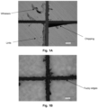
- dicing films comprising polyolefin-based substrate layers are prone to linting, formation of whiskers (fibrous off-cuts), chip fly and chipping during dicing (see Fig. 1A ), and fuzzy cutting edges (see Fig. 1 B) , overall resulting in poor quality cuts and reduced production yield.
- whiskers adhere to the side of the chip, the reliability of the resultant semiconductor element may be severely reduced.
- individual chips are picked up after positioning under recognition with a CCD camera, lints and whiskers may lead to recognition errors.
- the present invention provides a dicing tape comprising: a base layer, a first outer layer which is provided over the base layer and differs from the base layer, and an optional pressure-sensitive adhesive layer; wherein the base layer and the first outer layer comprise a polyolefin-based copolymer; and wherein the first outer layer comprises an organic or inorganic filler in an amount of 3 to 25 wt.-% based on the total weight of the respective layer.
- the present invention relates to a dicing method, comprising the steps of: mounting a semiconductor wafer onto the aforementioned dicing tape, dicing the semiconductor wafer, and separating the wafer from the dicing tape.
- the present invention generally relates to a dicing tape comprising: a base layer, a first outer layer which is provided over the base layer and differs from the base layer, and an optional pressure-sensitive adhesive layer; wherein the base layer and the first outer layer comprise a polyolefin-based copolymer; and wherein the first outer layer comprises an organic or inorganic filler in an amount of 3 to 25 wt.-% based on the total weight of the respective layer.
- the dicing tape does not comprise a polyvinyl chloride (PVC) resin or another chlorine-containing resin.
- PVC polyvinyl chloride
- the polyolefin-based copolymer has a melt flow rate (230°C/2.16 kg) determined according to ISO 11357-3 of 1.8 g/10 min or less, preferably 1.6 g/10 min or less.
- the first outer layer, the base layer and the second outer layer may independently comprise slip agents, preferably in an amount of 0.001 wt % to 1.0 wt %, based upon the weight of the respective layer.
- Slip agents include but are not limited to unsaturated fatty acid amides (e.g., erucamide, oleamide, and linoleamide); saturated fatty acid amides (e.g., palmitamide, stearamide, arachidamide, behenamide, stearyl stearamide, palmityl pamitamide, and stearyl arachidamide); saturated ethylene-bis-amides (e.g., stearamido-ethyl-stearamide, stearamido-ethyl-palmitamide, and palmitamido-ethyl-stearamide); unsaturated ethylene-bis-amides (e.g., ethylene-bis-stearamide, ethylene-bis-oleamide, stearyl-eruc
- esters of aromatic or aliphatic hydrocarbons e.g., pentaerythritol monooleate
- styrene-alpha-methyl styrene fluoro-containing polymers
- silicon compounds e.g., silicone oils
- sodium alkylsulfates, alkyl phosphoric acid esters stearates (such as zinc stearate); and mixtures thereof.
- the substrate layer in its entirety preferably has a tensile modulus of from 30 to 80 N/mm 2 in machine direction (MD), more preferably from 40 to 60 N/mm 2 , and/or a tensile modulus of from 20 to 60 N/mm 2 in transversal direction (TD), more preferably from 30 to 50 N/mm 2 .
- the substrate layer preferably has an elongation at break (MD) in the range of from 150 to 850%, more preferably from 200 to 700%, and/or an elongation at break (TD) in the range of from 200 to 900%, more preferably from 250 to 850%.
- the substrate layer may have a tensile strength (MD) in the range of from 15 to 45 N/mm 2 , more preferably from 20 to 40 N/mm 2 , and/or a tensile strength (TD) in the range of from 5 to 30 N/mm 2 , more preferably from 10 to 25 N/mm 2 .
- MD tensile strength
- TD tensile strength
- the tensile modulus, elongation at break and tensile strength may be determined in accordance to ISO 527 (1-3).
- the substrate layer exhibits a dimensional stability both in MD and TD of less than 10%, more preferably less than 5% and especially preferably less than 2%.
- the dimensional stability may be measured upon heating at 80°C for 1 h according to DIN 53377.
- a pressure-sensitive adhesive layer may be provided in contact with the first outer layer and/or the second outer layer (if present) for adhesion to the wafer. Also, a pressure-sensitive adhesive layer may be provided on each side of the substrate.
- the surface of the substrate on which the pressure-sensitive adhesive layer is provided may be subjected to a physical or chemical treatment to facilitate and/or improve bonding between the substrate and the adhesive layer, such as a plasma or corona discharge treatment.
- the pressure-sensitive adhesive layer is not particularly limited and its composition may be suitably selected by the skilled artisan from materials known in the art.
- the adhesive composition include rubber adhesives, acrylic adhesives, silicone adhesives, and thermoplastic elastomers such as styrenic elastomers and olefinic elastomers.
- the pressure-sensitive adhesive layer may be composed of radiation-curable adhesives of which the adhesive force decreases by radiation rays or heat-curable adhesives of which the adhesive force decreases by heat.
- the radiation-curable adhesives preferably include UV-curable adhesives.
- the pressure-sensitive adhesive layer preferably has a thickness of 1 to 100 ⁇ m, further preferably from 2 to 50 ⁇ m and especially preferably from 3 to 20 ⁇ m, in order to suppress an excessive increase in the amplitude of the vibration typically occurring during dicing of the semiconductor wafer, thus reducing dicing defects or chipping of the wafer.
- each adhesive face of the dicing tape may optionally be protected by a release liner or may be protected in a roll form wound with one release liner having a release face on each side.
- the release liner may be used as a protective material of the pressure-sensitive adhesive layer and may be peeled off in lamination of the sheet onto the workpiece.
- the release liner is not particularly limited and may comprise a release layer (release-treated layer) on at least one surface of the release liner substrate, a low-adhesive release liner comprising a fluorine polymer, and a low-adhesive release liner comprising a nonpolar polymer, for example.
- the total thickness of the dicing tape (excluding the optional release liner) is preferably in a range of from 50 to 300 ⁇ m and further preferably in a range of 80 to 200 ⁇ m.
- the thickness of the base layer preferably constitutes more than 50% of the total thickness of the base layer, the first outer layer and the second outer layer (if present).
- the base layer generally has a thickness in the range of from 30 to 150 ⁇ m.
- the base layer preferably has a thickness of from 45 to 150 ⁇ m
- the base layer in a three layer substrate configuration, preferably has a thickness of from 30 to 120 ⁇ m.
- the thickness of the first outer layer is typically in the range of from 2 to 80 ⁇ m, more preferably from 5 to 50 ⁇ m. Whereas in a two layer substrate configuration, the first outer layer preferably has a thickness of from 5 to 40 ⁇ m, in a three layer substrate configuration, the base layer preferably has a thickness of from 10 to 50 ⁇ m, especially preferably from 10 to 25 ⁇ m.
- the thickness of the second outer layer is typically in the range of from 2 to 80 ⁇ m, more preferably from 5 to 50 ⁇ m, further preferably from 7 to 50 ⁇ m, and especially preferably from 10 to 25 ⁇ m. If the first and the second outer layers have the same composition, it is preferred that the difference of their thicknesses is less than 10 ⁇ m, more preferably less than 5 ⁇ m, especially preferably less than 2 ⁇ m, such as 1 ⁇ m or less.
- the aforementioned thickness ranges provide a particularly favourable balance between tensile properties, stiffness and tear strength of the dicing tape and thus enable dicing with improved cut quality.
- the weight ratio of the polyolefin-based copolymer to the filler in the outer layer(s) is lower than the weight ratio of the polyolefin-based copolymer to the filler in the base layer, the elongation modulus of the outer layer(s) will be typically higher than that of the base layer, thin outer layers (e.g., with a thickness of from 5 to 40 ⁇ m (two-layer configuration) or 10 to 25 ⁇ m (three-layer configuration)) have the advantage that the tapes can be stretched with lower forces while maintaining good die-cuttability.
- the present invention relates to a dicing method, comprising the steps of: mounting a semiconductor wafer onto the dicing tape according to the fist embodiment, dicing the semiconductor wafer, optionally expanding the dicing tape and separating the diced semiconductor wafer from the dicing tape.
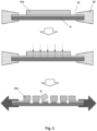
- FIG. 3 An exemplary dicing method is illustrated in Fig. 3 .
- a semiconductor wafer (31a) (which is not particularly limited and may be made of silicon, gallium or arsenic, for example), which is generally produced in a state having a large diameter, is first mounted onto the dicing tape described in conjunction with the first embodiment above, preferably by adhering the same to the pressure-sensitive adhesive layer (33) of the dicing tape.
- the dicing tape may be fixed in a holding frame (32).
- the semiconductor wafer (31a) is subjected, while sticking to the dicing tape, to dicing.
Landscapes
- Chemical & Material Sciences (AREA)
- Organic Chemistry (AREA)
- Health & Medical Sciences (AREA)
- Chemical Kinetics & Catalysis (AREA)
- Medicinal Chemistry (AREA)
- Polymers & Plastics (AREA)
- Dicing (AREA)
- Adhesive Tapes (AREA)
- Laminated Bodies (AREA)
Priority Applications (3)
| Application Number | Priority Date | Filing Date | Title |
|---|---|---|---|
| EP23219993.5A EP4574424A1 (fr) | 2023-12-22 | 2023-12-22 | Bande de découpage en dés et procédés associés |
| PCT/EP2024/084044 WO2025131619A1 (fr) | 2023-12-22 | 2024-11-29 | Bande de découpage en dés et procédés associés |
| TW113149822A TW202531354A (zh) | 2023-12-22 | 2024-12-20 | 切晶帶及相關方法 |
Applications Claiming Priority (1)
| Application Number | Priority Date | Filing Date | Title |
|---|---|---|---|
| EP23219993.5A EP4574424A1 (fr) | 2023-12-22 | 2023-12-22 | Bande de découpage en dés et procédés associés |
Publications (1)
| Publication Number | Publication Date |
|---|---|
| EP4574424A1 true EP4574424A1 (fr) | 2025-06-25 |
Family
ID=89429987
Family Applications (1)
| Application Number | Title | Priority Date | Filing Date |
|---|---|---|---|
| EP23219993.5A Pending EP4574424A1 (fr) | 2023-12-22 | 2023-12-22 | Bande de découpage en dés et procédés associés |
Country Status (3)
| Country | Link |
|---|---|
| EP (1) | EP4574424A1 (fr) |
| TW (1) | TW202531354A (fr) |
| WO (1) | WO2025131619A1 (fr) |
Citations (7)
| Publication number | Priority date | Publication date | Assignee | Title |
|---|---|---|---|---|
| EP0277598A2 (fr) * | 1987-01-28 | 1988-08-10 | Fuji Photo Film Co., Ltd. | Composition mélange-mère pour colorer |
| JPH05211234A (ja) | 1991-12-05 | 1993-08-20 | Lintec Corp | ウェハ貼着用粘着シートおよびウェハダイシング方法 |
| JPH07273173A (ja) * | 1994-03-28 | 1995-10-20 | Furukawa Electric Co Ltd:The | 半導体ウエハ固定用粘着テープ |
| US8728910B2 (en) | 2010-09-30 | 2014-05-20 | Mitsui Chemicals, Inc. | Expandable film, dicing film, and method of producing semiconductor device |
| KR101659057B1 (ko) | 2013-09-30 | 2016-09-22 | 주식회사 엘지화학 | 다이싱 필름 및 다이싱 다이본딩 필름 |
| US20170121569A1 (en) * | 2014-06-18 | 2017-05-04 | Lintec Corporation | Base film for dicing sheets and dicing sheet |
| WO2018123804A1 (fr) * | 2016-12-27 | 2018-07-05 | 三井・デュポンポリケミカル株式会社 | Base de film de découpage en dés et film de découpage en dés |
-
2023
- 2023-12-22 EP EP23219993.5A patent/EP4574424A1/fr active Pending
-
2024
- 2024-11-29 WO PCT/EP2024/084044 patent/WO2025131619A1/fr active Pending
- 2024-12-20 TW TW113149822A patent/TW202531354A/zh unknown
Patent Citations (7)
| Publication number | Priority date | Publication date | Assignee | Title |
|---|---|---|---|---|
| EP0277598A2 (fr) * | 1987-01-28 | 1988-08-10 | Fuji Photo Film Co., Ltd. | Composition mélange-mère pour colorer |
| JPH05211234A (ja) | 1991-12-05 | 1993-08-20 | Lintec Corp | ウェハ貼着用粘着シートおよびウェハダイシング方法 |
| JPH07273173A (ja) * | 1994-03-28 | 1995-10-20 | Furukawa Electric Co Ltd:The | 半導体ウエハ固定用粘着テープ |
| US8728910B2 (en) | 2010-09-30 | 2014-05-20 | Mitsui Chemicals, Inc. | Expandable film, dicing film, and method of producing semiconductor device |
| KR101659057B1 (ko) | 2013-09-30 | 2016-09-22 | 주식회사 엘지화학 | 다이싱 필름 및 다이싱 다이본딩 필름 |
| US20170121569A1 (en) * | 2014-06-18 | 2017-05-04 | Lintec Corporation | Base film for dicing sheets and dicing sheet |
| WO2018123804A1 (fr) * | 2016-12-27 | 2018-07-05 | 三井・デュポンポリケミカル株式会社 | Base de film de découpage en dés et film de découpage en dés |
Also Published As
| Publication number | Publication date |
|---|---|
| WO2025131619A1 (fr) | 2025-06-26 |
| TW202531354A (zh) | 2025-08-01 |
Similar Documents
| Publication | Publication Date | Title |
|---|---|---|
| KR101393878B1 (ko) | 확장성 필름, 다이싱 필름, 및 반도체 장치의 제조 방법 | |
| EP1892276A1 (fr) | Feuille adhésive sensible à la pression | |
| EP3125276A1 (fr) | Film de base pour feuille de découpage en dés, feuille de découpage en dés comportant ledit film de base, et procédé de fabrication dudit film de base | |
| JP6227494B2 (ja) | 半導体製造工程用粘着フィルムに使用する基材フィルム | |
| TW202432381A (zh) | 半導體製造膠帶用基材薄膜 | |
| EP3159914A1 (fr) | Film de base pour feuille de découpage en dés et feuille de découpage en dés | |
| JP2011061097A (ja) | ダイシング用プロセステープ。 | |
| JP5414085B1 (ja) | ダイシングシート用基材フィルムおよび当該基材フィルムを備えるダイシングシート | |
| EP3073515A1 (fr) | Film de base de feuille de découpage en dés et procédé de fabrication de film de base | |
| JP7311312B2 (ja) | ダイシングシート用基材フィルム | |
| EP4574424A1 (fr) | Bande de découpage en dés et procédés associés | |
| CN112778922B (zh) | 切割带和切割芯片接合薄膜 | |
| TW201319210A (zh) | 半導體裝置用之切割加工用黏著帶 | |
| JP6535508B2 (ja) | 半導工程用粘着フィルムに使用する基材フィルム | |
| TW201329190A (zh) | 黏著帶 | |
| US12552975B2 (en) | Carrier film for semi-conductor wafer processing | |
| JP5030461B2 (ja) | 半導体ウェハの裏面研削に用いる表面保護テープ用基材フィルム | |
| JP6281191B2 (ja) | 半導体製造工程用粘着テープ基材用樹脂フィルム | |
| JP7296805B2 (ja) | 均一拡張性フィルム | |
| JP7834246B1 (ja) | ダイシングシート用基材フィルム | |
| CN118103953A (zh) | 半导体制造胶带用基材薄膜 | |
| TWI920063B (zh) | 半導體晶圓加工載體膜 | |
| JP2023053783A (ja) | バックグラインド工程用フィルム及び粘着層付バックグラインド工程用フィルム | |
| WO2026069932A1 (fr) | Film de matériau de base pour feuille de découpage en dés | |
| KR100845978B1 (ko) | 반도체 다이싱용 점착테이프 |
Legal Events
| Date | Code | Title | Description |
|---|---|---|---|
| PUAI | Public reference made under article 153(3) epc to a published international application that has entered the european phase |
Free format text: ORIGINAL CODE: 0009012 |
|
| STAA | Information on the status of an ep patent application or granted ep patent |
Free format text: STATUS: THE APPLICATION HAS BEEN PUBLISHED |
|
| AK | Designated contracting states |
Kind code of ref document: A1 Designated state(s): AL AT BE BG CH CY CZ DE DK EE ES FI FR GB GR HR HU IE IS IT LI LT LU LV MC ME MK MT NL NO PL PT RO RS SE SI SK SM TR |
|
| STAA | Information on the status of an ep patent application or granted ep patent |
Free format text: STATUS: REQUEST FOR EXAMINATION WAS MADE |
|
| 17P | Request for examination filed |
Effective date: 20251210 |