EP4575593A1 - Bildgebungslinsenanordnungsmodul, kameramodul und elektronische vorrichtung - Google Patents
Bildgebungslinsenanordnungsmodul, kameramodul und elektronische vorrichtung Download PDFInfo
- Publication number
- EP4575593A1 EP4575593A1 EP24221038.3A EP24221038A EP4575593A1 EP 4575593 A1 EP4575593 A1 EP 4575593A1 EP 24221038 A EP24221038 A EP 24221038A EP 4575593 A1 EP4575593 A1 EP 4575593A1
- Authority
- EP
- European Patent Office
- Prior art keywords
- imaging lens
- lens assembly
- assembly module
- optically
- assembling
- Prior art date
- Legal status (The legal status is an assumption and is not a legal conclusion. Google has not performed a legal analysis and makes no representation as to the accuracy of the status listed.)
- Pending
Links
Images


Classifications
-
- G—PHYSICS
- G02—OPTICS
- G02B—OPTICAL ELEMENTS, SYSTEMS OR APPARATUS
- G02B1/00—Optical elements characterised by the material of which they are made; Optical coatings for optical elements
- G02B1/10—Optical coatings produced by application to, or surface treatment of, optical elements
- G02B1/11—Anti-reflection coatings
- G02B1/113—Anti-reflection coatings using inorganic layer materials only
- G02B1/115—Multilayers
-
- G—PHYSICS
- G02—OPTICS
- G02B—OPTICAL ELEMENTS, SYSTEMS OR APPARATUS
- G02B7/00—Mountings, adjusting means, or light-tight connections, for optical elements
-
- G—PHYSICS
- G02—OPTICS
- G02B—OPTICAL ELEMENTS, SYSTEMS OR APPARATUS
- G02B1/00—Optical elements characterised by the material of which they are made; Optical coatings for optical elements
- G02B1/10—Optical coatings produced by application to, or surface treatment of, optical elements
- G02B1/11—Anti-reflection coatings
- G02B1/118—Anti-reflection coatings having sub-optical wavelength surface structures designed to provide an enhanced transmittance, e.g. moth-eye structures
-
- G—PHYSICS
- G02—OPTICS
- G02B—OPTICAL ELEMENTS, SYSTEMS OR APPARATUS
- G02B5/00—Optical elements other than lenses
- G02B5/003—Light absorbing elements
-
- G—PHYSICS
- G02—OPTICS
- G02B—OPTICAL ELEMENTS, SYSTEMS OR APPARATUS
- G02B5/00—Optical elements other than lenses
- G02B5/02—Diffusing elements; Afocal elements
- G02B5/0205—Diffusing elements; Afocal elements characterised by the diffusing properties
- G02B5/021—Diffusing elements; Afocal elements characterised by the diffusing properties the diffusion taking place at the element's surface, e.g. by means of surface roughening or microprismatic structures
- G02B5/0221—Diffusing elements; Afocal elements characterised by the diffusing properties the diffusion taking place at the element's surface, e.g. by means of surface roughening or microprismatic structures the surface having an irregular structure
-
- G—PHYSICS
- G02—OPTICS
- G02B—OPTICAL ELEMENTS, SYSTEMS OR APPARATUS
- G02B7/00—Mountings, adjusting means, or light-tight connections, for optical elements
- G02B7/02—Mountings, adjusting means, or light-tight connections, for optical elements for lenses
-
- G—PHYSICS
- G03—PHOTOGRAPHY; CINEMATOGRAPHY; ANALOGOUS TECHNIQUES USING WAVES OTHER THAN OPTICAL WAVES; ELECTROGRAPHY; HOLOGRAPHY
- G03B—APPARATUS OR ARRANGEMENTS FOR TAKING PHOTOGRAPHS OR FOR PROJECTING OR VIEWING THEM; APPARATUS OR ARRANGEMENTS EMPLOYING ANALOGOUS TECHNIQUES USING WAVES OTHER THAN OPTICAL WAVES; ACCESSORIES THEREFOR
- G03B17/00—Details of cameras or camera bodies; Accessories therefor
- G03B17/02—Bodies
- G03B17/12—Bodies with means for supporting objectives, supplementary lenses, filters, masks, or turrets
-
- G—PHYSICS
- G03—PHOTOGRAPHY; CINEMATOGRAPHY; ANALOGOUS TECHNIQUES USING WAVES OTHER THAN OPTICAL WAVES; ELECTROGRAPHY; HOLOGRAPHY
- G03B—APPARATUS OR ARRANGEMENTS FOR TAKING PHOTOGRAPHS OR FOR PROJECTING OR VIEWING THEM; APPARATUS OR ARRANGEMENTS EMPLOYING ANALOGOUS TECHNIQUES USING WAVES OTHER THAN OPTICAL WAVES; ACCESSORIES THEREFOR
- G03B30/00—Camera modules comprising integrated lens units and imaging units, specially adapted for being embedded in other devices, e.g. mobile phones or vehicles
-
- H—ELECTRICITY
- H04—ELECTRIC COMMUNICATION TECHNIQUE
- H04N—PICTORIAL COMMUNICATION, e.g. TELEVISION
- H04N23/00—Cameras or camera modules comprising electronic image sensors; Control thereof
- H04N23/50—Constructional details
- H04N23/55—Optical parts specially adapted for electronic image sensors; Mounting thereof
-
- H—ELECTRICITY
- H04—ELECTRIC COMMUNICATION TECHNIQUE
- H04N—PICTORIAL COMMUNICATION, e.g. TELEVISION
- H04N23/00—Cameras or camera modules comprising electronic image sensors; Control thereof
- H04N23/57—Mechanical or electrical details of cameras or camera modules specially adapted for being embedded in other devices
-
- G—PHYSICS
- G02—OPTICS
- G02B—OPTICAL ELEMENTS, SYSTEMS OR APPARATUS
- G02B2207/00—Coding scheme for general features or characteristics of optical elements and systems of subclass G02B, but not including elements and systems which would be classified in G02B6/00 and subgroups
- G02B2207/101—Nanooptics
Definitions
- the present disclosure relates to an imaging lens assembly module and a camera module. More particularly, the present disclosure relates to an imaging lens assembly module and a camera module applicable to portable electronic devices.
- an imaging lens assembly module has an optical axis and includes an optical element, an assembling element and a low-reflection thin film, wherein the optical axis passes through the optical element.
- the assembling element is configured to be assembled with the optical element.
- the low-reflection thin film is disposed on a part of surfaces of the assembling element, and includes a nanostructure layer and a nanostructure matching layer.
- the nanostructure layer includes a plurality of ridged protrusions, wherein the ridged protrusions are arranged irregularly.
- the nanostructure matching layer is disposed between the assembling element and the nanostructure layer, and includes at least two optically rarer medium layers and at least one optically denser medium layer.
- the at least one optically denser medium layer is stacked between the at least two optically rarer medium layers, wherein a thickness of each of the at least two optically rarer medium layers is larger than 40 nm and less than 100 nm, a thickness of the at least one optically denser medium layer is larger than 1 nm and less than 33 nm, and a height of each of the ridged protrusions is larger than 80 nm and less than 300 nm.
- each of the at least two optically rarer medium layers is larger than 45 nm and less than 95 nm.
- each of the at least two optically rarer medium layers is larger than 48 nm and less than 85 nm.
- the thickness of the at least one optically denser medium layer is larger than 3 nm and less than 28 nm.
- the thickness of the at least one optically denser medium layer is larger than 3 nm and less than 25 nm.
- the imaging lens assembly module of the aforementioned aspect wherein the optical element is assembled on the assembling element, and the optical element is directly contacted with the assembling element.
- the imaging lens assembly module of the aforementioned aspect wherein the assembling element is made of an opaque plastic material to absorb a light incident into the assembling element.
- the at least two optically rarer medium layers include a silicon oxide material.
- the at least one optically denser medium layer includes a titanium oxide material.
- the ridged protrusions include an aluminum oxide material.
- the imaging lens assembly module further includes an adhering component that is disposed on the assembling element to assembly the imaging lens assembly module, wherein the adhering component is not directly contacted with the low-reflection thin film.
- an optical reflectance of the low-reflection thin film in a visible light wavelength range is R, and the following condition is satisfied: 0.0% ⁇ R ⁇ 0.6%.
- the imaging lens assembly module of the aforementioned aspect wherein the optical reflectance of the low-reflection thin film in the visible light wavelength range is R, and the following condition is satisfied: 0.0% ⁇ R ⁇ 0.4%.
- the imaging lens assembly module of the aforementioned aspect wherein the optical reflectance of the low-reflection thin film in the visible light wavelength range is R, and the following condition is satisfied: 0.0% ⁇ R ⁇ 0.3%.
- the imaging lens assembly module of the aforementioned aspect wherein the assembling element is disposed on a surface of the low-reflection thin film, and a value of CIELAB color space as claimed in the surface is L*a*b*, L* is a lightness, a* is a degree of red and green, b* is a degree of yellow and blue, and the following conditions are satisfied: 0.2 ⁇ L* ⁇ 2.7; -1.5 ⁇ a* ⁇ 2.0; and -4.0 ⁇ b* ⁇ 2.5.
- a camera module includes the imaging lens assembly module of the aforementioned aspect and an image sensor, wherein the image sensor is disposed on an image surface of the imaging lens assembly module.
- an electronic device includes the camera module of the aforementioned aspect.
- the present disclosure provides an imaging lens assembly module having an optical axis
- the imaging lens assembly module includes an optical element, an assembling element and a low-reflection thin film, wherein the optical axis passes through the optical element, and the assembling element is configured to be assembled with the optical element.
- the low-reflection thin film is disposed on a part of surfaces of the assembling element, and includes a nanostructure layer and a nanostructure matching layer.
- the nanostructure layer includes a plurality of ridged protrusions, wherein the ridged protrusions are arranged irregularly.
- the nanostructure matching layer is disposed between the assembling element and the nanostructure layer, and includes at least two optically rarer medium layers and at least one optically denser medium layer.
- the at least one optically denser medium layer is stacked between the at least two optically rarer medium layers, wherein a thickness of each of the at least two optically rarer medium layers is larger than 40 nm and less than 100 nm, a thickness of the at least one optically denser medium layer is larger than 1 nm and less than 33 nm, and a height of each of the ridged protrusions is larger than 80 nm and less than 300 nm. Therefore, it is favorable for improving a matching level of refractive indices between the assembling element and the nanostructure layer by the nanostructure matching layer, so that light can easily enter the assembling element from the outmost side of the nanostructure layer so as to keep a low reflectance.
- the present disclosure provides the low-reflection thin film with a high environmental tolerance by stacking the optically rarer medium layers, the optically denser medium layer and the nanostructure layer.
- the optically rarer medium layers and the optically denser medium layer of the nanostructure matching layer can be formed by stacking combinations of SiO 2 , MgF 2 , TiO 2 , Ta 2 O 5 , Cr 2 O 3 , HfO 2 , ZnO, AlN, Al 2 O 3 , Y 2 O 3 , CaF 2 , SiC, MgO and ZrO 2 , so that a tolerance to volatile substances of the low-reflection thin film can be improved and production processes can be optimized.
- the element proportions of the compounds above are not limited to the present disclosure, and can be different with different production processes.
- the ridged protrusions are with non-uniform heights, and heights of the ridged protrusions can be different.
- the optical element can be an optical lens element or an optical prism element, but the present disclosure is not limited thereto.
- the assembling element can be a lens barrel, a lens carrier, a retaining element or a prism carrier, but the present disclosure is not limited thereto.
- each of the at least two optically rarer medium layers can be larger than 45 nm and less than 95 nm. Therefore, it is favorable for improving the anti-reflecting efficacy of the low-reflection thin film by stacking the optically rarer medium layers and the optically denser medium layer with a certain thickness. Moreover, the thickness of each of the at least two optically rarer medium layers can be larger than 48 nm and less than 85 nm.
- the thickness of the at least one optically denser medium layer can be larger than 3 nm and less than 28 nm. Therefore, it is favorable for improving the anti-reflecting efficacy of the low-reflection thin film by stacking the optically rarer medium layers and the optically denser medium layer with a certain thickness. Moreover, the thickness of the optically denser medium layer can be larger than 3 nm and less than 25 nm.
- the optical element can be assembled on the assembling element, and the optical element can be directly contacted with the assembling element. Therefore, it is favorable for reducing a generation probability of the non-imaging light between the optical element and the assembling element.
- the assembling element can be made of an opaque plastic material to absorb the light incident into the assembling element. Therefore, it is favorable for improving the imaging quality of the imaging lens assembly module.
- the at least two optically rarer medium layers can include a silicon oxide material, and the silicon oxide material can be Si x O y , wherein proportions of silicon and oxygen are respectively x and y, the proportions can be different with different production processes. Therefore, a more stable process can be provided so as to ensure the mass production capability.
- the at least one optically denser medium layer can include a titanium oxide material, and the titanium oxide material can be Ti x O y , wherein proportions of titanium and oxygen are respectively x and y, the proportions can be different with different production processes. Therefore, an optical film material with a higher reflectance can be provided so as to reduce the complexity of a film layer design.
- the ridged protrusions can include an aluminum oxide material, the aluminum oxide material can be Al x O y , wherein proportions of aluminum and oxygen are respectively x and y, the proportions can be different with different production processes. Therefore, it is favorable for providing the durability and the structural stability of the low-reflection thin film so as to improve a product yield rate.
- the imaging lens assembly module can further include an adhering component, wherein the adhering component can be disposed on the assembling element to assembly the imaging lens assembly module, and the adhering component can be not directly contacted with the low-reflection thin film. Therefore, it is favorable for improving the assembling efficiency of the imaging lens assembly module so as to provide the assembling stability.
- an optical reflectance of the low-reflection thin film in a visible light wavelength range is R
- the following condition can be satisfied: 0.0% ⁇ R ⁇ 0.6%. Therefore, it is favorable for providing the low-reflection thin film with a high production yield rate.
- the following condition can be satisfied: 0.0% ⁇ R ⁇ 0.4%. Therefore, it is favorable for further increasing the efficiency of the assembling element in absorbing stray light.
- the following condition can be satisfied: 0.0% ⁇ R ⁇ 0.3%. Therefore, it is favorable for providing a high environmental tolerance of the low-reflection thin film and reducing the generation of stray light.
- the assembling element is disposed on a surface of the low-reflection thin film, wherein a value of CIELAB color space of the surface is L*a*b*, L* is a lightness, a* is a degree of red and green, b* is a degree of yellow and blue, and the following conditions can be satisfied: 0.2 ⁇ L* ⁇ 2.7; -1.5 ⁇ a* ⁇ 2.0; and -4.0 ⁇ b* ⁇ 2.5. Therefore, it is favorable for providing the stability in optical properties of the surface of the assembling element.
- Each of the aforementioned features of the imaging lens assembly module can be utilized in various combinations for achieving the corresponding effects.
- the present disclosure provides a camera module that includes the imaging lens assembly module of the aforementioned aspect and an image sensor, wherein the image sensor is disposed on an image surface of the imaging lens assembly module.
- the present disclosure provides an electronic device that includes the aforementioned camera module.
- Fig. 1A is a schematic view of a camera module 100 according to the 1st embodiment of the present disclosure.
- the camera module 100 includes an imaging lens assembly module (not shown) and an image sensor 110, wherein the image sensor 110 is disposed on an image surface (not shown) of the imaging lens assembly module.
- the imaging lens assembly module has an optical axis X, and the imaging lens assembly module includes an optical element 120, an assembling element 130 and a plurality of low-reflection thin films 140, wherein the optical axis X passes through the optical element 120, and the assembling element 130 is configured to be assembled with the optical element 120.
- the optical element 120 can be assembled on the assembling element 130, and the optical element 120 can be directly contacted with the assembling element 130.
- the assembling element 130 can be made of an opaque plastic material to absorb light incident into the assembling element 130.
- the assembling element 130 can include a first assembling component 131 and a second assembling component 132, wherein the first assembling component 131 surrounds and positions the optical element 120, the second assembling component 132 can be a retainer, and located on an image side of the optical element 120.
- the imaging lens assembly module can further include two adhering components 151, 152, wherein the adhering component 151 can be disposed on the first assembling component 131 of the assembling element 130 to assembly the imaging lens assembly module, and the adhering component 151 can be not directly contacted with the low-reflection thin films 140.
- the adhering component 152 is configured to position the second assembling component 132 in the first assembling component 131 and on the image side of the optical element 120.
- the optical element 120 can be an optical lens element or an optical prism element, but the present disclosure is not limited thereto.
- the assembling element 130 can be a lens barrel, a lens carrier, a retaining element or a prism carrier, but the present disclosure is not limited thereto.
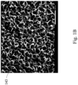
- Fig. 1B is a scanning electron microscope image of area 1B according to the 1st embodiment in Fig. 1A
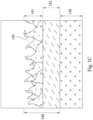
- Fig. 1C is a schematic view of a low-reflection thin film 140 and an assembling element 130 according to the 1st embodiment in Fig. 1A
- the low-reflection thin films 140 are disposed on a part of surfaces of the assembling element 130, which are surfaces of the first assembling component 131 facing towards an object side and a surface of the first assembling component 131 facing towards an image side.
- Each of the low-reflection thin films 140 includes a nanostructure layer 141 and a nanostructure matching layer 142.
- the nanostructure layer 141 includes a plurality of ridged protrusions 143, wherein the ridged protrusions 143 are arranged irregularly.
- the nanostructure matching layer 142 is disposed between the assembling element 130 and the nanostructure layer 141, and includes at least two optically rarer medium layers and at least one optically denser medium layer. Furthermore, the at least one optically denser medium layer is stacked between the at least two optically rarer medium layers.
- a thickness of each of the at least two optically rarer medium layers is larger than 40 nm and less than 100 nm, a thickness of the at least one optically denser medium layer is larger than 1 nm and less than 33 nm, and a height of each of the ridged protrusions 143 is larger than 80 nm and less than 300 nm.
- the thickness of each of the at least two optically rarer medium layers can be larger than 45 nm and less than 95 nm. Moreover, the thickness of each of the at least two optically rarer medium layers can be larger than 48 nm and less than 85 nm. The thickness of the at least one optically denser medium layer can be larger than 3 nm and less than 28 nm. Moreover, the thickness of the at least one optically denser medium layer can be larger than 3 nm and less than 25 nm. Furthermore, the at least two optically rarer medium layers can include a silicon oxide material, the at least one optically denser medium layer can include a titanium oxide material, and the ridged protrusions 143 can include an aluminum oxide material.
- Table 1 shows the material and the thickness of the nanostructure matching layer 142 of the Example 1 in the 1st embodiment.
- Values in Table 1 are the thickness of each of the at least two optically rarer medium layers and the thickness of the at least one optically denser medium layer, respectively.
- an optical reflectance of the low-reflection thin films 140 in a visible light wavelength range is R
- the following condition can be satisfied: 0.0% ⁇ R ⁇ 0.6%.
- the following condition can be satisfied: 0.0% ⁇ R ⁇ 0.4%.
- the following condition can be satisfied: 0.0% ⁇ R ⁇ 0.3%.
- the assembling element 130 is disposed on a surface of the low-reflection thin films 140, wherein a value of CIELAB color space of the surface is L*a*b*, L* is a lightness, a* is a degree of red and green, b* is a degree of yellow and blue, and the following conditions can be satisfied: 0.2 ⁇ L* ⁇ 2.7; -1.5 ⁇ a* ⁇ 2.0; and -4.0 ⁇ b* ⁇ 2.5.
- the mentioned parameters satisfy the following conditions in Table 2, and Table 2 shows values of CIELAB color space of the Example 1 in the 1st embodiment. Table 2, Example 1 in 1st embodiment Before heating After heating L* 0.90 1.26 a* -0.29 0.21 b* -1.83 -0.41
- Table 3 shows the thickness of each layer in the nanostructure matching layer 142 of the Example 2 in the 1st embodiment.
- the material of each layer in the nanostructure matching layer 142 of the Example 2 in the 1st embodiment and of the Example 1 in the 1st embodiment are the same or similar, the differences are the thickness of each of the at least two optically rarer medium layers and the thickness of the at least one optically denser medium layer.
- Table 4 shows values of CIELAB color space of the Example 2 in the 1st embodiment, the definitions of these parameters are the same as those stated in the Example 1 in the 1st embodiment, so an explanation will not be provided again.
- Table 4 Example 2 in 1st embodiment Before heating After heating L* 0.87 1.38 a* -0.23 0.20 b* -2.00 -0.35
- Table 5 shows the thickness of each layer in the nanostructure matching layer 142 of the Example 3 in the 1st embodiment.
- the material of each layer in the nanostructure matching layer 142 of the Example 3 in the 1st embodiment and of the Example 1 in the 1st embodiment are the same or similar, the differences are the thickness of each of the at least two optically rarer medium layers and the thickness of the at least one optically denser medium layer.
- Table 6 shows values of CIELAB color space of the Example 3 in the 1st embodiment, the definitions of these parameters are the same as those stated in the Example 1 in the 1st embodiment, so an explanation will not be provided again.
- Table 6 Example 3 in 1st embodiment Before heating After heating L* 0.76 2.48 a* 0.08 0.02 b* -0.22 2.42
- Table 7 shows the thickness of each layer in the nanostructure matching layer 142 of the Example 4 in the 1st embodiment.
- the material of each layer in the nanostructure matching layer 142 of the Example 4 in the 1st embodiment and of the Example 1 in the 1st embodiment are the same or similar, the differences are the thickness of each of the at least two optically rarer medium layers and the thickness of the at least one optically denser medium layer.
- Table 8 shows values of CIELAB color space of the Example 4 in the 1st embodiment, the definitions of these parameters are the same as those stated in the Example 1 in the 1st embodiment, so an explanation will not be provided again.
- Table 8 Example 4 in 1st embodiment Before heating After heating L* 0.94 2.52 a* -0.61 -0.10 b* 0.32 2.14
- Example 2 in the 1st embodiment the Example 3 in the 1st embodiment, and the Example 4 in the 1st embodiment are the same as the component structures and arrangements according to the Example 1 in the 1st embodiment, and will not be described again herein.
- Fig. 2 is a schematic view of a camera module 200 according to the 2nd embodiment of the present disclosure.
- the camera module 200 includes an imaging lens assembly module (not shown) and an image sensor 210, wherein the image sensor 210 is disposed on an image surface (not shown) of the imaging lens assembly module.
- the imaging lens assembly module has an optical axis X, and the imaging lens assembly module includes an optical element 220, an assembling element 230 and a plurality of low-reflection thin films 240, wherein the optical axis X passes through the optical element 220, and the assembling element 230 is configured to be assembled with the optical element 220.
- the assembling element 230 can include a first assembling component 231 and a second assembling component 232, wherein the first assembling component 231 surrounds and positions the optical element 220, the second assembling component 232 can be a retainer and located on an image side of the optical element 220.
- the imaging lens assembly module can further include two adhering components 251, 252, wherein the adhering component 251 can be disposed on the first assembling component 231 to assembly the imaging lens assembly module, and the adhering component 251 can be not directly contacted with the low-reflection thin films 240.
- the adhering component 252 is configured to position the second assembling component 232 in the first assembling component 231 and on the image side of the optical element 220.
- the low-reflection thin films 240 are disposed on a part of surfaces of the assembling element 230, which are a surface of the first assembling component 231 facing towards an object side and a surface of the second assembling component 232 facing towards an image side.
- Fig. 3 is a schematic view of a camera module 300 according to the 3rd embodiment of the present disclosure.
- the camera module 300 includes an imaging lens assembly module (not shown) and an image sensor 310, wherein the image sensor 310 is disposed on an image surface (not shown) of the imaging lens assembly module.
- the imaging lens assembly module has an optical axis X, and the imaging lens assembly module includes an optical element 320, an assembling element 330 and a plurality of low-reflection thin films 340, wherein the optical axis X passes through the optical element 320, and the assembling element 330 is configured to be assembled with the optical element 320.
- the optical element 320 can include a first optical component 321 and a second optical component 322.
- the assembling element 330 can include a first assembling component 331, a second assembling component 332, a third assembling component 333, and a fourth assembling component 334, wherein the first assembling component 331 surrounds the first optical component 321, the second assembling component 332 can be a retainer and located on an image side of the first optical component 321, the third assembling component 333 is configured to position the first optical component 321 and the second optical component 322, and the fourth assembling component 334 is located on an image side of the second optical component 322.
- the imaging lens assembly module can further include three adhering components 351, 352, 353 wherein the adhering component 351 can be disposed on the first assembling component 331, the adhering component 352 is configured to position the second assembling component 332 in the first assembling component 331 and on the image side of the first optical component 321, and the adhering component 353 can be disposed on the fourth assembling component 334 so as to assembly the imaging lens assembly module. Moreover, the adhering components 351, 353 can be not directly contacted with the low-reflection thin films 340.
- the low-reflection thin films 340 are disposed on a part of surfaces of the assembling element 330, which are a surface of the first assembling component 331 facing towards an image side, a surface of the second assembling component 332 facing towards the image side, a surface of the third assembling component 333 facing towards the image side, and a surface of the fourth assembling component 334 facing towards an object side.
- Fig. 4 is a schematic view of a camera module 400 according to the 4th embodiment of the present disclosure.
- the camera module 400 includes an imaging lens assembly module (not shown) and an image sensor 410, wherein the image sensor 410 is disposed on an image surface (not shown) of the imaging lens assembly module.
- the imaging lens assembly module has an optical axis X, and the imaging lens assembly module includes an optical element 420, an assembling element 430 and a low-reflection thin film 440, wherein the optical axis X passes through the optical element 420, and the assembling element 430 is configured to be assembled with the optical element 420.
- the imaging lens assembly module can further include an adhering component 450, wherein the adhering component 450 can be disposed on the assembling element 430 to assembly the imaging lens assembly module, and the adhering component 450 can be not directly contacted with the low-reflection thin film 440. Further, the low-reflection thin film 440 is disposed on a part of surfaces of the assembling element 430, which is a surface of the assembling element 430 facing towards an object side.
- the component structures and arrangements according to the 4th embodiment are the same as the component structures and arrangements according to the 1st embodiment, and will not be described again herein.
- Fig. 5 is a schematic view of a camera module 500 according to the 5th embodiment of the present disclosure.
- the camera module 500 includes an imaging lens assembly module (not shown) and an image sensor 510, wherein the image sensor 510 is disposed on an image surface (not shown) of the imaging lens assembly module.
- the imaging lens assembly module has an optical axis X, and the imaging lens assembly module includes an optical element 520, an assembling element 530 and a low-reflection thin film 540, wherein the optical axis X passes through the optical element 520, and the assembling element 530 is configured to be assembled with the optical element 520.
- the imaging lens assembly module can further include an adhering component 550, wherein the adhering component 550 can be disposed on the assembling element 530 to assembly the imaging lens assembly module, and the adhering component 550 can be not directly contacted with the low-reflection thin film 540. Further, the low-reflection thin film 540 is disposed on a part of surfaces of the assembling element 530, which is a surface of the assembling element 530 facing towards an object side.
- the component structures and arrangements according to the 5th embodiment are the same as the component structures and arrangements according to the 1st embodiment, and will not be described again herein.
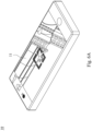
- Fig. 6A is a schematic view of an electronic device 10 according to the 6th embodiment of the present disclosure
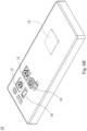
- Fig. 6B is another schematic view of the electronic device 10 according to the 6th embodiment in Fig. 6A
- the electronic device 10 is a smart phone
- the electronic device 10 includes camera modules and a user interface 11, wherein the camera module includes an imaging lens assembly module (not shown) and an image sensor (not shown), wherein the image sensor is disposed on an image surface (not shown) of the imaging lens assembly module, and the imaging lens assembly module includes an optical element, an assembling element and a low-reflection thin film.
- the camera modules are an ultra-wide angle camera module 12, a high resolution camera module 13 and a telephoto camera module 14, and the user interface 11 is a touch screen, but the present disclosure is not limited thereto.
- the camera module can be the camera module according to any one of the aforementioned 1st embodiment to the 5th embodiment, but the present disclosure is not limited thereto.
- a user enters a shooting mode via the user interface 11, wherein the user interface 11 is configured to display an image, and the shooting angle can be manually adjusted to switch to different camera modules.
- the imaging light is gathered on an image sensor, and an electronic signal about an image is output to an image signal processor (ISP) 15.
- ISP image signal processor
- the electronic device 10 can further include an optical anti-shake mechanism (not shown). Furthermore, the electronic device 10 can further include at least one focusing assisting module (not shown) and at least one sensing element (not shown).
- the focusing assisting module can be a flash module (not shown) for compensating a color temperature, an infrared distance measurement component, a laser focus module and so on.
- the sensing element can have functions for sensing physical momentum and kinetic energy, such as an accelerator, a gyroscope, a Hall Effect element, to sense shaking or jitters applied by hands of the users or external environments.
- the camera module of the electronic device 10 equipped with an auto-focusing mechanism and the optical anti-shake mechanism can be enhanced to achieve the superior image quality.
- the electronic device 10 according to the present disclosure can have a capturing function with multiple modes, such as taking optimized selfies, high dynamic range (HDR) under a low light condition, 4K resolution recording and so on.
- the user can visually see a captured image of the camera via the user interface 11 and manually operate the view finding range on the user interface 11 to achieve the autofocus function of what you see is what you get.
- the camera module, the optical anti-shake mechanism, the sensing element and the focusing assisting module can be disposed on a flexible printed circuit board (FPC) (not shown) and electrically connected to the image signal processor 15 and other related components, via a connector (not shown) to perform a capturing process.
- FPC flexible printed circuit board
- the way of firstly disposing the camera module and related components on the flexible printed circuit board and secondly integrating the circuit thereof into the main board of the electronic device via the connector can satisfy the requirements of the mechanical design and the circuit layout of the limited space inside the electronic device, and obtain more margins.
- the autofocus function of the camera module can also be controlled more flexibly via the touch screen of the electronic device.
- the electronic device 10 can include a plurality of sensing elements and a plurality of focusing assisting modules.
- the sensing elements and the focusing assisting modules are disposed on the flexible printed circuit board and at least one other flexible printed circuit board (not shown) and electrically connected to the image signal processor 15 and other related components, via corresponding connectors to perform the capturing process.
- the sensing elements and the focusing assisting modules can also be disposed on the main board of the electronic device or carrier boards of other types according to requirements of the mechanical design and the circuit layout.
- the electronic device 10 can further include, but not be limited to, a display, a control unit, a storage unit, a random access memory (RAM), a read-only memory (ROM), or the combination thereof.
- Fig. 6C is a schematic view of an image captured via the electronic device 10 according to the 6th embodiment in Fig. 6A .
- the larger range of the image can be captured via the ultra-wide angle camera module 12, and the ultra-wide angle camera module 12 has the function of accommodating wider range of the scene.
- Fig. 6D is a schematic view of another image captured via the electronic device 10 according to the 6th embodiment in Fig. 6A .
- the image of the certain range with the high resolution can be captured via the high resolution camera module 13, and the high resolution camera module 13 has the function of the high resolution and the low deformation.
- Fig. 6E is a schematic view of another image captured via the electronic device 10 according to the 6th embodiment in Fig. 6A .
- the telephoto camera module 14 has the enlarging function of the high magnification, and the distant image can be captured and enlarged with high magnification via the telephoto camera module 14.
- the zooming function can be obtained via the electronic device 10, when the scene is captured via the camera module with different focal lengths cooperated with the function of image processing.
- Fig. 7 is a schematic view of an electronic device 20 according to the 7th embodiment of the present disclosure.
- the electronic device 20 is a smart phone
- the electronic device 20 includes the camera module, wherein the camera module includes an imaging lens assembly module and an image sensor, the image sensor is disposed on an image surface of the imaging lens assembly module, and the imaging lens assembly module includes an optical element, an assembling element and a low-reflection thin film.
- the camera modules can be ultra-wide angle camera modules 22a, 22b, wide angle camera modules 23a,23b, telephoto camera modules 24a, 24b, 24c, 24d and a Time-Of-Flight (TOF) module 26.
- the TOF module 26 can be another type of the camera module, and the disposition is not limited thereto.
- the camera module can be the camera module according to any one of the aforementioned 1st embodiment to the 5th embodiment, but the present disclosure is not limited thereto.
- the telephoto camera modules 24c, 24d are configured to fold the light, but the present disclosure is not limited thereto.
- the electronic device 20 can further include an optical anti-shake mechanism
- the electronic device 20 can further include at least one focusing assisting module (not shown) and at least one sensing element (not shown).
- the focusing assisting module can be a flash module 27 for compensating a color temperature, an infrared distance measurement component, a laser focus module and so on.
- the sensing element can have functions for sensing physical momentum and kinetic energy, such as an accelerator, a gyroscope, a Hall Effect element, to sense shaking or jitters applied by hands of the users or external environments. Accordingly, the camera module of the electronic device 20 equipped with an auto-focusing mechanism and the optical anti-shake mechanism can be enhanced to achieve the superior image quality.
- the electronic device 20 according to the present disclosure can have a capturing function with multiple modes, such as taking optimized selfies, High Dynamic Range (HDR) under a low light condition, 4K Resolution recording and so on.
- HDR High Dynamic Range
- Fig. 8A is a schematic view of a camera module 31 applied to a vehicle 30 according to the 8th embodiment of the present disclosure
- Fig. 8B is a schematic view of a camera module 31 configured on the vehicle 30 according to the 8th embodiment in Fig. 8A
- Fig. 8C is another schematic view of a camera module (not shown) configured on the vehicle 30 according to the 8th embodiment in Fig. 8A
- a number of camera modules 31 is six, the camera modules 31 are vehicle camera modules, and the camera module can be the camera module according to any one of the aforementioned 1st embodiment to the 5th embodiment, but the present disclosure is not limited thereto.
- two of the camera modules 31 are disposed under a left rearview mirror and a right rearview mirror, respectively, which can for capturing the image information with a visual angle ⁇ .
- the visual angle ⁇ can satisfy the following condition: 40 degrees ⁇ ⁇ ⁇ 90 degrees. Therefore, the image information within a left lane and a right lane can be captured.
- another two of the camera modules 31 can be disposed in an inner space of the vehicle 30.
- the aforementioned two of the camera modules 31 on a location close to the rearview mirror inside the vehicle 30 and a location close to the rear car window, respectively.
- the camera modules 31 can be further disposed on the rearview mirrors on the left side and the right side except the mirror surface, respectively, but the present disclosure is not limited thereto.
- another two of the camera modules 31 can be disposed on a front end of the vehicle 30 and a rear end of the vehicle 30, respectively.
- the camera modules 31 By disposing the camera modules 31 on the front end and the rear end of the vehicle 30 and under the rearview mirror on the left side of the vehicle 30 and the right side of the vehicle 30, it is favorable for the drivers obtaining the external space information in addition to the driving seat, such as the external space informations I1, I2, I3, I4, but the present disclosure is not limited thereto. Therefore, more visual angles can be provided to reduce the blind spot, so that the driving safety can be improved.
- the traffic information outside of the vehicle 30 can be recognized by disposing the camera modules 31 on the periphery of the vehicle 30, so that the function of the automatic driving assistance can be achieved.
Landscapes
- Physics & Mathematics (AREA)
- General Physics & Mathematics (AREA)
- Optics & Photonics (AREA)
- Chemical & Material Sciences (AREA)
- Inorganic Chemistry (AREA)
- Engineering & Computer Science (AREA)
- Multimedia (AREA)
- Signal Processing (AREA)
- Studio Devices (AREA)
- Transforming Light Signals Into Electric Signals (AREA)
Applications Claiming Priority (2)
| Application Number | Priority Date | Filing Date | Title |
|---|---|---|---|
| US202363613181P | 2023-12-21 | 2023-12-21 | |
| TW113131719A TW202526433A (zh) | 2023-12-21 | 2024-08-23 | 成像鏡頭模組、相機模組及電子裝置 |
Publications (1)
| Publication Number | Publication Date |
|---|---|
| EP4575593A1 true EP4575593A1 (de) | 2025-06-25 |
Family
ID=93926083
Family Applications (1)
| Application Number | Title | Priority Date | Filing Date |
|---|---|---|---|
| EP24221038.3A Pending EP4575593A1 (de) | 2023-12-21 | 2024-12-18 | Bildgebungslinsenanordnungsmodul, kameramodul und elektronische vorrichtung |
Country Status (3)
| Country | Link |
|---|---|
| US (1) | US20250208318A1 (de) |
| EP (1) | EP4575593A1 (de) |
| CN (2) | CN120195831A (de) |
Citations (5)
| Publication number | Priority date | Publication date | Assignee | Title |
|---|---|---|---|---|
| US20150177419A1 (en) * | 2013-12-23 | 2015-06-25 | Largan Precision Co., Ltd. | Optical lens and mobile terminal |
| US20180011224A1 (en) * | 2015-03-31 | 2018-01-11 | Fujifilm Corporation | Antireflection film and method of producing the same |
| US20210165136A1 (en) * | 2019-11-29 | 2021-06-03 | Largan Precision Co., Ltd. | Imaging lens assembly, camera module and electronic device |
| US20220407993A1 (en) * | 2021-06-10 | 2022-12-22 | Largan Precision Co., Ltd. | Camera module, electronic device and vehicle instrument |
| US20230305200A1 (en) * | 2022-03-23 | 2023-09-28 | Largan Precision Co., Ltd. | Low reflection layer, optical lens assembly, imaging apparatus and electronic device |
-
2024
- 2024-11-15 CN CN202411634746.8A patent/CN120195831A/zh active Pending
- 2024-11-15 CN CN202422796143.XU patent/CN223426913U/zh active Active
- 2024-12-01 US US18/964,624 patent/US20250208318A1/en active Pending
- 2024-12-18 EP EP24221038.3A patent/EP4575593A1/de active Pending
Patent Citations (5)
| Publication number | Priority date | Publication date | Assignee | Title |
|---|---|---|---|---|
| US20150177419A1 (en) * | 2013-12-23 | 2015-06-25 | Largan Precision Co., Ltd. | Optical lens and mobile terminal |
| US20180011224A1 (en) * | 2015-03-31 | 2018-01-11 | Fujifilm Corporation | Antireflection film and method of producing the same |
| US20210165136A1 (en) * | 2019-11-29 | 2021-06-03 | Largan Precision Co., Ltd. | Imaging lens assembly, camera module and electronic device |
| US20220407993A1 (en) * | 2021-06-10 | 2022-12-22 | Largan Precision Co., Ltd. | Camera module, electronic device and vehicle instrument |
| US20230305200A1 (en) * | 2022-03-23 | 2023-09-28 | Largan Precision Co., Ltd. | Low reflection layer, optical lens assembly, imaging apparatus and electronic device |
Also Published As
| Publication number | Publication date |
|---|---|
| US20250208318A1 (en) | 2025-06-26 |
| CN223426913U (zh) | 2025-10-10 |
| CN120195831A (zh) | 2025-06-24 |
Similar Documents
| Publication | Publication Date | Title |
|---|---|---|
| KR102760679B1 (ko) | 카메라 모듈, 전자 장치 및 차량 기기 | |
| EP4276501A1 (de) | Abbildungslinsenanordnung, kameramodul und elektronische vorrichtung | |
| EP4102263B1 (de) | Kameramodul und elektronische vorrichtung | |
| US20240272407A1 (en) | Optical imaging module and electronic device | |
| US20230324588A1 (en) | Metal light blocking element, imaging lens assembly module and electronic device | |
| CN220671792U (zh) | 光路转折元件、相机模块与电子装置 | |
| US20240295721A1 (en) | Imaging lens assembly and electronic device | |
| EP4575593A1 (de) | Bildgebungslinsenanordnungsmodul, kameramodul und elektronische vorrichtung | |
| US20240111139A1 (en) | Imaging lens assembly module, camera module and electronic device | |
| EP4163691B1 (de) | Optisches bildgebungssystem, kameramodul und elektronische vorrichtung | |
| EP4592717A1 (de) | Abbildungslinsenanordnung und elektronische vorrichtung | |
| US20250189695A1 (en) | Image sensor module, camera module and electronic device | |
| US12610120B2 (en) | Imaging lens module, camera module and electronic device having a plurality of columnar structures for reducing reflection | |
| CN221860734U (zh) | 成像镜头与电子装置 | |
| US20240272406A1 (en) | Optical imaging module, camera module and electronic device | |
| US20250052933A1 (en) | Imaging lens assembly, imaging lens assembly module and electronic device | |
| US12523923B2 (en) | Light path folding element, camera module and electronic device | |
| US20250013038A1 (en) | Imaging lens assembly module, camera module and electronic device | |
| TW202526433A (zh) | 成像鏡頭模組、相機模組及電子裝置 |
Legal Events
| Date | Code | Title | Description |
|---|---|---|---|
| PUAI | Public reference made under article 153(3) epc to a published international application that has entered the european phase |
Free format text: ORIGINAL CODE: 0009012 |
|
| STAA | Information on the status of an ep patent application or granted ep patent |
Free format text: STATUS: REQUEST FOR EXAMINATION WAS MADE |
|
| 17P | Request for examination filed |
Effective date: 20241218 |
|
| AK | Designated contracting states |
Kind code of ref document: A1 Designated state(s): AL AT BE BG CH CY CZ DE DK EE ES FI FR GB GR HR HU IE IS IT LI LT LU LV MC ME MK MT NL NO PL PT RO RS SE SI SK SM TR |