EP4576140A1 - Composant électronique multicouche - Google Patents
Composant électronique multicouche Download PDFInfo
- Publication number
- EP4576140A1 EP4576140A1 EP24211150.8A EP24211150A EP4576140A1 EP 4576140 A1 EP4576140 A1 EP 4576140A1 EP 24211150 A EP24211150 A EP 24211150A EP 4576140 A1 EP4576140 A1 EP 4576140A1
- Authority
- EP
- European Patent Office
- Prior art keywords
- dielectric layer
- moles
- sub
- component
- electronic component
- Prior art date
- Legal status (The legal status is an assumption and is not a legal conclusion. Google has not performed a legal analysis and makes no representation as to the accuracy of the status listed.)
- Pending
Links
Images




Classifications
-
- H—ELECTRICITY
- H01—ELECTRIC ELEMENTS
- H01G—CAPACITORS; CAPACITORS, RECTIFIERS, DETECTORS, SWITCHING DEVICES, LIGHT-SENSITIVE OR TEMPERATURE-SENSITIVE DEVICES OF THE ELECTROLYTIC TYPE
- H01G4/00—Fixed capacitors; Processes of their manufacture
- H01G4/30—Stacked capacitors
-
- C—CHEMISTRY; METALLURGY
- C04—CEMENTS; CONCRETE; ARTIFICIAL STONE; CERAMICS; REFRACTORIES
- C04B—LIME, MAGNESIA; SLAG; CEMENTS; COMPOSITIONS THEREOF, e.g. MORTARS, CONCRETE OR LIKE BUILDING MATERIALS; ARTIFICIAL STONE; CERAMICS; REFRACTORIES; TREATMENT OF NATURAL STONE
- C04B35/00—Shaped ceramic products characterised by their composition; Ceramics compositions; Processing powders of inorganic compounds preparatory to the manufacturing of ceramic products
- C04B35/01—Shaped ceramic products characterised by their composition; Ceramics compositions; Processing powders of inorganic compounds preparatory to the manufacturing of ceramic products based on oxide ceramics
- C04B35/46—Shaped ceramic products characterised by their composition; Ceramics compositions; Processing powders of inorganic compounds preparatory to the manufacturing of ceramic products based on oxide ceramics based on titanium oxides or titanates
- C04B35/462—Shaped ceramic products characterised by their composition; Ceramics compositions; Processing powders of inorganic compounds preparatory to the manufacturing of ceramic products based on oxide ceramics based on titanium oxides or titanates based on titanates
- C04B35/465—Shaped ceramic products characterised by their composition; Ceramics compositions; Processing powders of inorganic compounds preparatory to the manufacturing of ceramic products based on oxide ceramics based on titanium oxides or titanates based on titanates based on alkaline earth metal titanates
- C04B35/468—Shaped ceramic products characterised by their composition; Ceramics compositions; Processing powders of inorganic compounds preparatory to the manufacturing of ceramic products based on oxide ceramics based on titanium oxides or titanates based on titanates based on alkaline earth metal titanates based on barium titanates
-
- C—CHEMISTRY; METALLURGY
- C04—CEMENTS; CONCRETE; ARTIFICIAL STONE; CERAMICS; REFRACTORIES
- C04B—LIME, MAGNESIA; SLAG; CEMENTS; COMPOSITIONS THEREOF, e.g. MORTARS, CONCRETE OR LIKE BUILDING MATERIALS; ARTIFICIAL STONE; CERAMICS; REFRACTORIES; TREATMENT OF NATURAL STONE
- C04B35/00—Shaped ceramic products characterised by their composition; Ceramics compositions; Processing powders of inorganic compounds preparatory to the manufacturing of ceramic products
- C04B35/01—Shaped ceramic products characterised by their composition; Ceramics compositions; Processing powders of inorganic compounds preparatory to the manufacturing of ceramic products based on oxide ceramics
- C04B35/46—Shaped ceramic products characterised by their composition; Ceramics compositions; Processing powders of inorganic compounds preparatory to the manufacturing of ceramic products based on oxide ceramics based on titanium oxides or titanates
- C04B35/462—Shaped ceramic products characterised by their composition; Ceramics compositions; Processing powders of inorganic compounds preparatory to the manufacturing of ceramic products based on oxide ceramics based on titanium oxides or titanates based on titanates
- C04B35/465—Shaped ceramic products characterised by their composition; Ceramics compositions; Processing powders of inorganic compounds preparatory to the manufacturing of ceramic products based on oxide ceramics based on titanium oxides or titanates based on titanates based on alkaline earth metal titanates
- C04B35/468—Shaped ceramic products characterised by their composition; Ceramics compositions; Processing powders of inorganic compounds preparatory to the manufacturing of ceramic products based on oxide ceramics based on titanium oxides or titanates based on titanates based on alkaline earth metal titanates based on barium titanates
- C04B35/4682—Shaped ceramic products characterised by their composition; Ceramics compositions; Processing powders of inorganic compounds preparatory to the manufacturing of ceramic products based on oxide ceramics based on titanium oxides or titanates based on titanates based on alkaline earth metal titanates based on barium titanates based on BaTiO3 perovskite phase
-
- H—ELECTRICITY
- H01—ELECTRIC ELEMENTS
- H01G—CAPACITORS; CAPACITORS, RECTIFIERS, DETECTORS, SWITCHING DEVICES, LIGHT-SENSITIVE OR TEMPERATURE-SENSITIVE DEVICES OF THE ELECTROLYTIC TYPE
- H01G4/00—Fixed capacitors; Processes of their manufacture
- H01G4/002—Details
- H01G4/005—Electrodes
- H01G4/012—Form of non-self-supporting electrodes
-
- H—ELECTRICITY
- H01—ELECTRIC ELEMENTS
- H01G—CAPACITORS; CAPACITORS, RECTIFIERS, DETECTORS, SWITCHING DEVICES, LIGHT-SENSITIVE OR TEMPERATURE-SENSITIVE DEVICES OF THE ELECTROLYTIC TYPE
- H01G4/00—Fixed capacitors; Processes of their manufacture
- H01G4/002—Details
- H01G4/018—Dielectrics
- H01G4/06—Solid dielectrics
- H01G4/08—Inorganic dielectrics
- H01G4/12—Ceramic dielectrics
- H01G4/1209—Ceramic dielectrics characterised by the ceramic dielectric material
- H01G4/1218—Ceramic dielectrics characterised by the ceramic dielectric material based on titanium oxides or titanates
- H01G4/1227—Ceramic dielectrics characterised by the ceramic dielectric material based on titanium oxides or titanates based on alkaline earth titanates
-
- C—CHEMISTRY; METALLURGY
- C04—CEMENTS; CONCRETE; ARTIFICIAL STONE; CERAMICS; REFRACTORIES
- C04B—LIME, MAGNESIA; SLAG; CEMENTS; COMPOSITIONS THEREOF, e.g. MORTARS, CONCRETE OR LIKE BUILDING MATERIALS; ARTIFICIAL STONE; CERAMICS; REFRACTORIES; TREATMENT OF NATURAL STONE
- C04B2235/00—Aspects relating to ceramic starting mixtures or sintered ceramic products
- C04B2235/02—Composition of constituents of the starting material or of secondary phases of the final product
- C04B2235/30—Constituents and secondary phases not being of a fibrous nature
- C04B2235/32—Metal oxides, mixed metal oxides, or oxide-forming salts thereof, e.g. carbonates, nitrates, (oxy)hydroxides, chlorides
- C04B2235/3205—Alkaline earth oxides or oxide forming salts thereof, e.g. beryllium oxide
- C04B2235/3206—Magnesium oxides or oxide-forming salts thereof
-
- C—CHEMISTRY; METALLURGY
- C04—CEMENTS; CONCRETE; ARTIFICIAL STONE; CERAMICS; REFRACTORIES
- C04B—LIME, MAGNESIA; SLAG; CEMENTS; COMPOSITIONS THEREOF, e.g. MORTARS, CONCRETE OR LIKE BUILDING MATERIALS; ARTIFICIAL STONE; CERAMICS; REFRACTORIES; TREATMENT OF NATURAL STONE
- C04B2235/00—Aspects relating to ceramic starting mixtures or sintered ceramic products
- C04B2235/02—Composition of constituents of the starting material or of secondary phases of the final product
- C04B2235/30—Constituents and secondary phases not being of a fibrous nature
- C04B2235/32—Metal oxides, mixed metal oxides, or oxide-forming salts thereof, e.g. carbonates, nitrates, (oxy)hydroxides, chlorides
- C04B2235/3224—Rare earth oxide or oxide forming salts thereof, e.g. scandium oxide
-
- C—CHEMISTRY; METALLURGY
- C04—CEMENTS; CONCRETE; ARTIFICIAL STONE; CERAMICS; REFRACTORIES
- C04B—LIME, MAGNESIA; SLAG; CEMENTS; COMPOSITIONS THEREOF, e.g. MORTARS, CONCRETE OR LIKE BUILDING MATERIALS; ARTIFICIAL STONE; CERAMICS; REFRACTORIES; TREATMENT OF NATURAL STONE
- C04B2235/00—Aspects relating to ceramic starting mixtures or sintered ceramic products
- C04B2235/02—Composition of constituents of the starting material or of secondary phases of the final product
- C04B2235/30—Constituents and secondary phases not being of a fibrous nature
- C04B2235/32—Metal oxides, mixed metal oxides, or oxide-forming salts thereof, e.g. carbonates, nitrates, (oxy)hydroxides, chlorides
- C04B2235/3231—Refractory metal oxides, their mixed metal oxides, or oxide-forming salts thereof
- C04B2235/3232—Titanium oxides or titanates, e.g. rutile or anatase
-
- C—CHEMISTRY; METALLURGY
- C04—CEMENTS; CONCRETE; ARTIFICIAL STONE; CERAMICS; REFRACTORIES
- C04B—LIME, MAGNESIA; SLAG; CEMENTS; COMPOSITIONS THEREOF, e.g. MORTARS, CONCRETE OR LIKE BUILDING MATERIALS; ARTIFICIAL STONE; CERAMICS; REFRACTORIES; TREATMENT OF NATURAL STONE
- C04B2235/00—Aspects relating to ceramic starting mixtures or sintered ceramic products
- C04B2235/02—Composition of constituents of the starting material or of secondary phases of the final product
- C04B2235/30—Constituents and secondary phases not being of a fibrous nature
- C04B2235/32—Metal oxides, mixed metal oxides, or oxide-forming salts thereof, e.g. carbonates, nitrates, (oxy)hydroxides, chlorides
- C04B2235/3231—Refractory metal oxides, their mixed metal oxides, or oxide-forming salts thereof
- C04B2235/3239—Vanadium oxides, vanadates or oxide forming salts thereof, e.g. magnesium vanadate
-
- C—CHEMISTRY; METALLURGY
- C04—CEMENTS; CONCRETE; ARTIFICIAL STONE; CERAMICS; REFRACTORIES
- C04B—LIME, MAGNESIA; SLAG; CEMENTS; COMPOSITIONS THEREOF, e.g. MORTARS, CONCRETE OR LIKE BUILDING MATERIALS; ARTIFICIAL STONE; CERAMICS; REFRACTORIES; TREATMENT OF NATURAL STONE
- C04B2235/00—Aspects relating to ceramic starting mixtures or sintered ceramic products
- C04B2235/02—Composition of constituents of the starting material or of secondary phases of the final product
- C04B2235/30—Constituents and secondary phases not being of a fibrous nature
- C04B2235/32—Metal oxides, mixed metal oxides, or oxide-forming salts thereof, e.g. carbonates, nitrates, (oxy)hydroxides, chlorides
- C04B2235/3231—Refractory metal oxides, their mixed metal oxides, or oxide-forming salts thereof
- C04B2235/3241—Chromium oxides, chromates, or oxide-forming salts thereof
-
- C—CHEMISTRY; METALLURGY
- C04—CEMENTS; CONCRETE; ARTIFICIAL STONE; CERAMICS; REFRACTORIES
- C04B—LIME, MAGNESIA; SLAG; CEMENTS; COMPOSITIONS THEREOF, e.g. MORTARS, CONCRETE OR LIKE BUILDING MATERIALS; ARTIFICIAL STONE; CERAMICS; REFRACTORIES; TREATMENT OF NATURAL STONE
- C04B2235/00—Aspects relating to ceramic starting mixtures or sintered ceramic products
- C04B2235/02—Composition of constituents of the starting material or of secondary phases of the final product
- C04B2235/30—Constituents and secondary phases not being of a fibrous nature
- C04B2235/32—Metal oxides, mixed metal oxides, or oxide-forming salts thereof, e.g. carbonates, nitrates, (oxy)hydroxides, chlorides
- C04B2235/3262—Manganese oxides, manganates, rhenium oxides or oxide-forming salts thereof, e.g. MnO
- C04B2235/3267—MnO2
-
- C—CHEMISTRY; METALLURGY
- C04—CEMENTS; CONCRETE; ARTIFICIAL STONE; CERAMICS; REFRACTORIES
- C04B—LIME, MAGNESIA; SLAG; CEMENTS; COMPOSITIONS THEREOF, e.g. MORTARS, CONCRETE OR LIKE BUILDING MATERIALS; ARTIFICIAL STONE; CERAMICS; REFRACTORIES; TREATMENT OF NATURAL STONE
- C04B2235/00—Aspects relating to ceramic starting mixtures or sintered ceramic products
- C04B2235/02—Composition of constituents of the starting material or of secondary phases of the final product
- C04B2235/30—Constituents and secondary phases not being of a fibrous nature
- C04B2235/32—Metal oxides, mixed metal oxides, or oxide-forming salts thereof, e.g. carbonates, nitrates, (oxy)hydroxides, chlorides
- C04B2235/327—Iron group oxides, their mixed metal oxides, or oxide-forming salts thereof
- C04B2235/3272—Iron oxides or oxide forming salts thereof, e.g. hematite, magnetite
-
- C—CHEMISTRY; METALLURGY
- C04—CEMENTS; CONCRETE; ARTIFICIAL STONE; CERAMICS; REFRACTORIES
- C04B—LIME, MAGNESIA; SLAG; CEMENTS; COMPOSITIONS THEREOF, e.g. MORTARS, CONCRETE OR LIKE BUILDING MATERIALS; ARTIFICIAL STONE; CERAMICS; REFRACTORIES; TREATMENT OF NATURAL STONE
- C04B2235/00—Aspects relating to ceramic starting mixtures or sintered ceramic products
- C04B2235/02—Composition of constituents of the starting material or of secondary phases of the final product
- C04B2235/30—Constituents and secondary phases not being of a fibrous nature
- C04B2235/32—Metal oxides, mixed metal oxides, or oxide-forming salts thereof, e.g. carbonates, nitrates, (oxy)hydroxides, chlorides
- C04B2235/327—Iron group oxides, their mixed metal oxides, or oxide-forming salts thereof
- C04B2235/3275—Cobalt oxides, cobaltates or cobaltites or oxide forming salts thereof, e.g. bismuth cobaltate, zinc cobaltite
-
- C—CHEMISTRY; METALLURGY
- C04—CEMENTS; CONCRETE; ARTIFICIAL STONE; CERAMICS; REFRACTORIES
- C04B—LIME, MAGNESIA; SLAG; CEMENTS; COMPOSITIONS THEREOF, e.g. MORTARS, CONCRETE OR LIKE BUILDING MATERIALS; ARTIFICIAL STONE; CERAMICS; REFRACTORIES; TREATMENT OF NATURAL STONE
- C04B2235/00—Aspects relating to ceramic starting mixtures or sintered ceramic products
- C04B2235/02—Composition of constituents of the starting material or of secondary phases of the final product
- C04B2235/30—Constituents and secondary phases not being of a fibrous nature
- C04B2235/32—Metal oxides, mixed metal oxides, or oxide-forming salts thereof, e.g. carbonates, nitrates, (oxy)hydroxides, chlorides
- C04B2235/327—Iron group oxides, their mixed metal oxides, or oxide-forming salts thereof
- C04B2235/3279—Nickel oxides, nickalates, or oxide-forming salts thereof
-
- C—CHEMISTRY; METALLURGY
- C04—CEMENTS; CONCRETE; ARTIFICIAL STONE; CERAMICS; REFRACTORIES
- C04B—LIME, MAGNESIA; SLAG; CEMENTS; COMPOSITIONS THEREOF, e.g. MORTARS, CONCRETE OR LIKE BUILDING MATERIALS; ARTIFICIAL STONE; CERAMICS; REFRACTORIES; TREATMENT OF NATURAL STONE
- C04B2235/00—Aspects relating to ceramic starting mixtures or sintered ceramic products
- C04B2235/02—Composition of constituents of the starting material or of secondary phases of the final product
- C04B2235/30—Constituents and secondary phases not being of a fibrous nature
- C04B2235/32—Metal oxides, mixed metal oxides, or oxide-forming salts thereof, e.g. carbonates, nitrates, (oxy)hydroxides, chlorides
- C04B2235/3281—Copper oxides, cuprates or oxide-forming salts thereof, e.g. CuO or Cu2O
-
- C—CHEMISTRY; METALLURGY
- C04—CEMENTS; CONCRETE; ARTIFICIAL STONE; CERAMICS; REFRACTORIES
- C04B—LIME, MAGNESIA; SLAG; CEMENTS; COMPOSITIONS THEREOF, e.g. MORTARS, CONCRETE OR LIKE BUILDING MATERIALS; ARTIFICIAL STONE; CERAMICS; REFRACTORIES; TREATMENT OF NATURAL STONE
- C04B2235/00—Aspects relating to ceramic starting mixtures or sintered ceramic products
- C04B2235/02—Composition of constituents of the starting material or of secondary phases of the final product
- C04B2235/30—Constituents and secondary phases not being of a fibrous nature
- C04B2235/32—Metal oxides, mixed metal oxides, or oxide-forming salts thereof, e.g. carbonates, nitrates, (oxy)hydroxides, chlorides
- C04B2235/3284—Zinc oxides, zincates, cadmium oxides, cadmiates, mercury oxides, mercurates or oxide forming salts thereof
-
- C—CHEMISTRY; METALLURGY
- C04—CEMENTS; CONCRETE; ARTIFICIAL STONE; CERAMICS; REFRACTORIES
- C04B—LIME, MAGNESIA; SLAG; CEMENTS; COMPOSITIONS THEREOF, e.g. MORTARS, CONCRETE OR LIKE BUILDING MATERIALS; ARTIFICIAL STONE; CERAMICS; REFRACTORIES; TREATMENT OF NATURAL STONE
- C04B2235/00—Aspects relating to ceramic starting mixtures or sintered ceramic products
- C04B2235/02—Composition of constituents of the starting material or of secondary phases of the final product
- C04B2235/30—Constituents and secondary phases not being of a fibrous nature
- C04B2235/34—Non-metal oxides, non-metal mixed oxides, or salts thereof that form the non-metal oxides upon heating, e.g. carbonates, nitrates, (oxy)hydroxides, chlorides
- C04B2235/3418—Silicon oxide, silicic acids or oxide forming salts thereof, e.g. silica sol, fused silica, silica fume, cristobalite, quartz or flint
-
- C—CHEMISTRY; METALLURGY
- C04—CEMENTS; CONCRETE; ARTIFICIAL STONE; CERAMICS; REFRACTORIES
- C04B—LIME, MAGNESIA; SLAG; CEMENTS; COMPOSITIONS THEREOF, e.g. MORTARS, CONCRETE OR LIKE BUILDING MATERIALS; ARTIFICIAL STONE; CERAMICS; REFRACTORIES; TREATMENT OF NATURAL STONE
- C04B2235/00—Aspects relating to ceramic starting mixtures or sintered ceramic products
- C04B2235/02—Composition of constituents of the starting material or of secondary phases of the final product
- C04B2235/50—Constituents or additives of the starting mixture chosen for their shape or used because of their shape or their physical appearance
- C04B2235/54—Particle size related information
- C04B2235/5418—Particle size related information expressed by the size of the particles or aggregates thereof
- C04B2235/5445—Particle size related information expressed by the size of the particles or aggregates thereof submicron sized, i.e. from 0,1 to 1 micron
-
- C—CHEMISTRY; METALLURGY
- C04—CEMENTS; CONCRETE; ARTIFICIAL STONE; CERAMICS; REFRACTORIES
- C04B—LIME, MAGNESIA; SLAG; CEMENTS; COMPOSITIONS THEREOF, e.g. MORTARS, CONCRETE OR LIKE BUILDING MATERIALS; ARTIFICIAL STONE; CERAMICS; REFRACTORIES; TREATMENT OF NATURAL STONE
- C04B2235/00—Aspects relating to ceramic starting mixtures or sintered ceramic products
- C04B2235/65—Aspects relating to heat treatments of ceramic bodies such as green ceramics or pre-sintered ceramics, e.g. burning, sintering or melting processes
- C04B2235/652—Reduction treatment
-
- C—CHEMISTRY; METALLURGY
- C04—CEMENTS; CONCRETE; ARTIFICIAL STONE; CERAMICS; REFRACTORIES
- C04B—LIME, MAGNESIA; SLAG; CEMENTS; COMPOSITIONS THEREOF, e.g. MORTARS, CONCRETE OR LIKE BUILDING MATERIALS; ARTIFICIAL STONE; CERAMICS; REFRACTORIES; TREATMENT OF NATURAL STONE
- C04B2235/00—Aspects relating to ceramic starting mixtures or sintered ceramic products
- C04B2235/65—Aspects relating to heat treatments of ceramic bodies such as green ceramics or pre-sintered ceramics, e.g. burning, sintering or melting processes
- C04B2235/658—Atmosphere during thermal treatment
- C04B2235/6582—Hydrogen containing atmosphere
-
- C—CHEMISTRY; METALLURGY
- C04—CEMENTS; CONCRETE; ARTIFICIAL STONE; CERAMICS; REFRACTORIES
- C04B—LIME, MAGNESIA; SLAG; CEMENTS; COMPOSITIONS THEREOF, e.g. MORTARS, CONCRETE OR LIKE BUILDING MATERIALS; ARTIFICIAL STONE; CERAMICS; REFRACTORIES; TREATMENT OF NATURAL STONE
- C04B2235/00—Aspects relating to ceramic starting mixtures or sintered ceramic products
- C04B2235/70—Aspects relating to sintered or melt-casted ceramic products
- C04B2235/74—Physical characteristics
- C04B2235/78—Grain sizes and shapes, product microstructures, e.g. acicular grains, equiaxed grains, platelet-structures
- C04B2235/785—Submicron sized grains, i.e. from 0,1 to 1 micron
-
- C—CHEMISTRY; METALLURGY
- C04—CEMENTS; CONCRETE; ARTIFICIAL STONE; CERAMICS; REFRACTORIES
- C04B—LIME, MAGNESIA; SLAG; CEMENTS; COMPOSITIONS THEREOF, e.g. MORTARS, CONCRETE OR LIKE BUILDING MATERIALS; ARTIFICIAL STONE; CERAMICS; REFRACTORIES; TREATMENT OF NATURAL STONE
- C04B2235/00—Aspects relating to ceramic starting mixtures or sintered ceramic products
- C04B2235/70—Aspects relating to sintered or melt-casted ceramic products
- C04B2235/80—Phases present in the sintered or melt-cast ceramic products other than the main phase
-
- H—ELECTRICITY
- H01—ELECTRIC ELEMENTS
- H01G—CAPACITORS; CAPACITORS, RECTIFIERS, DETECTORS, SWITCHING DEVICES, LIGHT-SENSITIVE OR TEMPERATURE-SENSITIVE DEVICES OF THE ELECTROLYTIC TYPE
- H01G4/00—Fixed capacitors; Processes of their manufacture
- H01G4/002—Details
- H01G4/018—Dielectrics
- H01G4/06—Solid dielectrics
- H01G4/08—Inorganic dielectrics
- H01G4/12—Ceramic dielectrics
- H01G4/1209—Ceramic dielectrics characterised by the ceramic dielectric material
-
- Y—GENERAL TAGGING OF NEW TECHNOLOGICAL DEVELOPMENTS; GENERAL TAGGING OF CROSS-SECTIONAL TECHNOLOGIES SPANNING OVER SEVERAL SECTIONS OF THE IPC; TECHNICAL SUBJECTS COVERED BY FORMER USPC CROSS-REFERENCE ART COLLECTIONS [XRACs] AND DIGESTS
- Y02—TECHNOLOGIES OR APPLICATIONS FOR MITIGATION OR ADAPTATION AGAINST CLIMATE CHANGE
- Y02E—REDUCTION OF GREENHOUSE GAS [GHG] EMISSIONS, RELATED TO ENERGY GENERATION, TRANSMISSION OR DISTRIBUTION
- Y02E60/00—Enabling technologies; Technologies with a potential or indirect contribution to GHG emissions mitigation
- Y02E60/13—Energy storage using capacitors
Definitions
- the present disclosure relates to a multilayer electronic component.
- a multilayer ceramic capacitor (MLCC), a multilayer electronic component may be a chip condenser mounted on the printed circuit boards of various electronic products including image display devices such as a liquid crystal display (LCD) and a plasma display panel (PDP), a computer, a smartphone, a mobile phone, or the like, charging or discharging electricity therein or therefrom.
- image display devices such as a liquid crystal display (LCD) and a plasma display panel (PDP), a computer, a smartphone, a mobile phone, or the like, charging or discharging electricity therein or therefrom.
- LCD liquid crystal display
- PDP plasma display panel
- An embodiment of the present disclosure is to provide a multilayer electronic component satisfying X7R or X7S properties.
- An embodiment of the present disclosure is to provide a multilayer electronic component having improved capacitance.
- FIG. 1 is a perspective diagram illustrating a multilayer electronic component according to an embodiment.
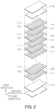
- FIG. 2 is an exploded perspective diagram illustrating a lamination structure of an internal electrode according to an embodiment.
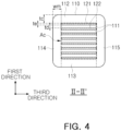
- FIG. 4 is a cross-sectional diagram taken along line II-II' in FIG. 1 .
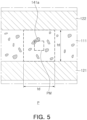
- FIG. 5 is an enlarged diagram illustrating region P in FIG. 3 .
- FIG. 6 is an enlarged diagram illustrating region PM in FIG. 5 .
- FIG. 7 is a diagram illustrating a core-shell dielectric grain according to an embodiment.
- a multilayer ceramic capacitor will be described as an example of a multilayer electronic component, but an embodiment thereof is not limited thereto, and the multilayer ceramic capacitor may be applied to various multilayer electronic components, such as an inductor, a piezoelectric element, a varistor, or a thermistor.
- the raw material forming the dielectric layer 111 is not limited as long as sufficient capacitance may be obtained therewith, and generally, a perovskite (ABO 3 ) material may be used, and for example, a barium titanate material, a lead composite perovskite material, or a strontium titanate material may be used.
- a perovskite (ABO 3 ) material may be used, and for example, a barium titanate material, a lead composite perovskite material, or a strontium titanate material may be used.
- various ceramic additives, organic solvents, binders, and dispersants may be added to particles such as barium titanate (BaTiO 3 ) depending on the purpose of the embodiment.
- the dielectric layer 111 may be formed using a dielectric material such as barium titanate (BaTiO 3 ), the dielectric layer 111 may include a dielectric microstructure after firing.
- the dielectric microstructure may include a plurality of grains, a grain boundary disposed between the adjacent grains, and a triple point at which three or more of the grain boundaries are in contact with each other, and a plurality of triple points may be included.
- At least one of the plurality of grains may include a core 11 and a core-shell dielectric grain 10 having a shell 12 structure surrounding at least a portion of the core 11, and may include a dielectric grain which may not have a core-shell structure, but an embodiment thereof is not limited thereto.
- a thickness td of the dielectric layer 111 may not be limited to any particular example.
- the thickness of the dielectric layer 111 may be 10.0 um or less. Also, to implement miniaturization and high capacitance of the multilayer electronic component 100, the thickness of the dielectric layer 111 may be 3.0 um or less. To easily implement ultra-miniaturization and high capacitance, the thickness of the dielectric layer 111 may be 1.0 um or less, preferably 0.6 um or less, and more preferably 0.4 um or less.
- the thickness td of dielectric layer 111 may indicate the thickness td of at least one of the plurality of dielectric layer 111.
- the thickness te of the internal electrodes 121 and 122 may not be limited to any particular example.
- the average thickness td of the dielectric layer 111 is less than twice the average thickness te of the internal electrodes 121 and 122, the average thickness of the dielectric layer, which is the distance between the internal electrodes, may be reduced such that the breakdown voltage may decrease, and a short may occur between the internal electrodes.
- the thickness tc of the cover portion 112 and 113 may not be limited to any particular example.
- the average size of the cover portions 112 and 113 may be measured by scanning a cross-section in the first and second directions of the body 110 using a scanning electron microscope (SEM) at a magnification of 10,000. More specifically, the average size may indicate the average value calculated by measuring the sizes, in the first direction, at 10 points at an equal distance in the second direction in the scanned image of the cover portion.
- SEM scanning electron microscope
- the average size, in the first direction, of the cover portion measured by the above method may be substantially the same as the average size, in the first direction, of the cover portion in the cross-section in the first and third directions of the body 110.
- the multilayer electronic component 100 may include side margin portions 114 and 115 disposed on both end-surfaces in the third direction of the body 110.
- the side margin portions 114 and 115 may include a first side margin portion 114 disposed on the fifth surface 5 and a second side margin portion 115 disposed on the sixth surface 6 of the body 110.
- the side margin portions 114 and 115 may refer to a region between both end-surfaces in the third direction of the first and second internal electrodes 121 and 122 and the boundary surface of the body 110 with respect to the cross-section in the first and third directions of the body 110.
- the side margin portions 114 and 115 may be formed by forming the internal electrodes 121 and 122 on a ceramic green sheet by applying a conductive paste other than the region in which the side margin portions 114 and 115 are formed, cutting the laminated internal electrodes 121 and 122 to expose the fifth and sixth surfaces 5 and 6 of the body 110 to prevent a step difference caused by the internal electrodes 121 and 122, and laminating a single dielectric layer 111 or two or more dielectric layers 111 in the third direction on both end-surfaces in the third direction of the capacitance forming portion Ac.
- the side margin portions 114 and 115 may prevent damages to the internal electrodes 121 and 122 due to physical or chemical stress.
- the first side margin portion 114 and the second side margin portion 115 may not include the internal electrodes 121 and 122 and may include the same material as that of the dielectric layer 111. That is, the first side margin portion 114 and the second side margin portion 115 may include a ceramic material, for example, a barium titanate (BaTiO 3 ) ceramic material.
- a ceramic material for example, a barium titanate (BaTiO 3 ) ceramic material.
- the width wm of the first and second side margin portions 114 and 115 may not be limited to any particular example.
- the width wm of the side margin portions 114 and 115 may be 100 ⁇ m or less, preferably 30 um or less, and may be more preferably 20 ⁇ m or less in an ultra-small product.
- the width wm of the side margin portions 114 and 115 may refer to the size of the side margin portions 114 and 115 in the third direction. Also, the width wm of the side margin portions 114 and 115 may refer to the average width wm of the side margin portions 114 and 115, and the average size in the third direction of the side margin portions 114 and 115.
- the ceramic electronic component 100 may have two external electrodes 131 and 132, but the number of the external electrodes 131 and 132 or the shape thereof may be varied depending on the forms of the internal electrode 121 and 122 or other purposes.
- the external electrodes 131 and 132 may be disposed on the body 110 and may be connected to the internal electrodes 121 and 122.
- the external electrodes 131 and 132 may be disposed on the third and fourth surfaces 3 and 4 of the body 110, respectively, and may include first and second external electrodes 131 and 132 connected to the first and second internal electrodes 121 and 122, respectively. That is, the first external electrode 131 may be disposed on the third surface 3 of the body and may be connected to the first internal electrode 121, and the second external electrode 132 may be disposed on the fourth surface 4 of the body and may be connected to the second internal electrode 122.
- the external electrodes 131 and 132 may extend and be disposed on portions of the first and second surfaces 1 and 2 of the body 110, or may extend and be disposed on a portion of the fifth and sixth surfaces 5 and 6 of the body 110. That is, the first external electrode 131 may be disposed on a portion of the first, second, fifth, and sixth surfaces 1, 2, 5, and 6 of the body 110, and the third surface 3 of the body 110, and the second external electrode 132 may be disposed on a portion of the first, second, fifth, and sixth surfaces 1, 2, 5, and 6 of the body 110, and the third surface 3 of the body 110.
- the external electrodes 131 and 132 may be formed of any material having electrical conductivity, such as metal, and a specific material may be determined in consideration of electrical properties and structural stability, and the external electrodes 131 and 132 may have a multilayer structure.
- the external electrodes 131 and 132 may include an electrode layer disposed on the body 110 and a plating layer disposed on the electrode layer.
- the electrode layer may include first electrode layers 131a and 132a, which may be fired electrodes including a first conductive metal and glass, or second electrode layers 131b and 132b, which may be resin-based electrodes including a second conductive metal and resin.
- the conductive metal included in the first electrode layers 131a and 132a may be referred to as a first conductive metal
- the conductive metal included in the second electrode layers 131b and 132b may be referred to as a second conductive metal.
- the first conductive metal and second conductive metal may be the same or different from each other, and when a plurality of conductive metals are included, only a portion thereof may include the same conductive metal, but an embodiment thereof is not limited thereto.
- the electrode layers 131a and 132a, 131b, and 132b may be formed by forming a fired electrode and a resin-based electrode on the body 110 in order.
- the electrode layers 131a and 132a, 131b, and 132b may be formed by transferring a sheet including a conductive metal onto the body, or may be formed by transferring a sheet including a conductive metal onto the fired electrode.
- a material having excellent electrical conductivity may be used as a conductive metal included in the electrode layers 131a and 132a, 131b, and 132b.
- the conductive metal may include one or more selected from a group consisting of nickel (Ni), copper (Cu), palladium (Pd), silver (Ag), gold (Au), platinum (Pt), tin (Sn), tungsten (W), titanium (Ti) and alloys thereof, but an embodiment thereof is not limited thereto.
- the electrode layers 131a and 132a, 131b, and 132b may have a two-layer structure including the first electrode layers 131a and 132a and the second electrode layers 131b and 132b, and accordingly, the external electrodes 131 and 132 may include first electrode layers 131a and 132a including a first conductive metal and glass, and second electrode layers 131b and 132b disposed on the first electrode layers 131a and 132a and including a second conductive metal and resin.
- the first electrode layers 131a and 132a may improve bondability with the body 110 by including glass, and the second electrode layers 131b and 132b may improve warpage strength by including resin.
- the first conductive metal included in the first electrode layers 131a and 132a is not limited to any particular example as long as the material may be electrically connected to the internal electrodes 121 and 122 to form capacitance, and for example, the first conductive metal may include one or more selected from a group consisting of nickel (Ni), copper (Cu), palladium (Pd), silver (Ag), gold (Au), platinum (Pt), tin (Sn), tungsten (W), titanium (Ti) and alloys thereof.
- the first electrode layers 131a and 132a may be formed by applying a conductive paste prepared by adding glass frit to the first conductive metal particles and firing the paste.
- the second conductive metal included in the second electrode layers 131b and 132b may allow the layers to be electrically connected to the first electrode layers 131a and 132a.
- the conductive metal included in the second electrode layers 131b and 132b is not limited to any particular example as long as the material may be electrically connected to the electrode layers 131a and 132a, and may include one or more selected from a group consisting of nickel (Ni), copper (Cu), palladium (Pd), silver (Ag), gold (Au), platinum (Pt), tin (Sn), tungsten (W), titanium (Ti) and alloys thereof.
- the second conductive metal included in the second electrode layers 131b and 132b may include one or more of spherical particles and flake-type particles.
- the conductive metal may only include flake-type particles, only spherical particles, or may be a mixture of flake-type particles and spherical particles.
- spherical particles may include shapes not completely spherical, for example, shapes in which the length ratio (major axis/minor axis) between the major axis and the minor axis is 1.45 or higher.
- Flake-type particles may refer to particles having a flat and elongated shape, and are not limited to any particular example, and for example, a length ratio of the major axis between the minor axis (major axis/minor axis) may be 1.95 or more.
- the length of the major axis and the minor axis of the spherical particles and the flake-type particles may be measured from an image obtained by scanning the cross-sections in first and second direction of the central portion in the third direction of the multilayer electronic component using a scanning electron microscope (SEM).
- the resin included in the second electrode layers 131b and 132b may secure bondability and may absorb impacts.
- the resin included in the second electrode layers 131b and 132b is not limited to any particular example as long as the resin has bondability and impact absorption properties and may be mixed with second conductive metal particles to create a paste, and may include, for example, an epoxy resin
- the second electrode layers 131b and 132b may include a plurality of metal particles, an intermetallic compound and resin.
- an intermetallic compound By including an intermetallic compound, electrical connectivity with the first electrode layers 131a and 132a may be improved.
- the intermetallic compound may improve electrical connectivity by connecting a plurality of metal particles to each other, and may surround a plurality of metal particles and may connect the metal particles to each other.
- the intermetallic compound may include a metal having a melting point lower than a curing temperature of resin. That is, as the intermetallic compound may include a metal having a melting point lower than the curing temperature of resin, the metal having a melting point lower than the curing temperature of the resin may melt during a drying and curing process, may form an intermetallic compound with a portion of the metal particles and may surround the metal particles. In this case, the intermetallic compound may include a low melting point metal, preferably below 300°C.
- Sn having a melting point of 213-220°C may be included.
- Sn may be melted, and the melted Sn may wet metal particles at high melting points such as Ag, Ni, or Cu by capillary action, may react with a portion of Ag, Ni or Cu metal particles and may form intermetallic compounds such as Ag 3 Sn, Ni 3 Sn 4 , Cu 6 Sn 5 , or Cu 3 Sn.
- Ag, Ni or Cu not participating in the reaction may remain in the form of metal particles.
- the plurality of metal particles may include one or more of Ag, Ni and Cu
- the intermetallic compound may include one or more of Ag 3 Sn, Ni 3 Sn 4 , Cu 6 Sn 5 and Cu 3 Sn.
- the plating layers 131c and 132c may improve mounting properties.
- the type of the plating layers 131c and 132c is not limited to any particular example, and the plating layers 131c and 132c may be single-layer plating layers 131c and 132c including at least one of nickel (Ni), tin (Sn), palladium (Pd), and alloys thereof, and may be formed in a plurality of layers.
- the plating layers 131c and 132c may be Ni plating layers or Sn plating layers, and Ni plating layers and Sn plating layers may be formed in order on the electrode layers, and a Sn plating layer, a Ni plating layer, and a Sn plating layer may be formed in order.
- the plating layers 131c and 132c may include a plurality of Ni plating layers and/or a plurality of Sn plating layers.
- the size of the multilayer electronic component 100 may not be limited to any particular example.
- the number of laminates may need to be increased by reducing the thickness of the dielectric layer and the internal electrode, such that the effect described in the embodiments may be noticeable in the multilayer electronic component 100 having a size of 3216 (length ⁇ width: 3.2 mm ⁇ 1.6 mm) or less.
- multilayer electronic component 100 according to an embodiment of the present disclosure will be described in greater detail.
- the dielectric layer 111 may include a secondary phase 141 including Si
- the secondary phase 141 including Si may include the secondary phase 141a (e.g., first secondary phase) including Si having a cross-sectional area of 0.01 ⁇ m 2 or more, and a secondary phase 141b (e.g., second secondary phase) including Si having a cross-sectional area of less than 0.01 ⁇ m 2 .
- the description of the secondary phase 141 including Si may correspond to the description of the secondary phase 141a including Si having a cross-sectional area of 0.01 ⁇ m 2 or more and the description of the secondary phase 141b including Si having a cross-sectional area of less than 0.01 ⁇ m 2 .
- the dielectric layer 111 may include five or more secondary phases 141a having a cross-sectional area of 0.01 ⁇ m 2 or more within the td ⁇ m ⁇ td ⁇ m region and including Si.
- the dielectric layer 111 includes five or more secondary phases 141a having a cross-sectional area of 0.01 ⁇ m 2 or more within the td ⁇ m ⁇ td ⁇ m region and including Si, high-temperature accelerated life reliability may be improved.
- high-temperature accelerated life reliability properties in which mean time to failure (MTTF) under temperature of 150°C and electric field of 10 V/ ⁇ m is 100 hours or more.
- the number of the secondary phases 141a having a cross-sectional area of 0.01 ⁇ m 2 or more within the td um ⁇ td ⁇ m region and including Si is not limited to any particular example, and to prevent other properties from deteriorating, the number of the secondary phases 141a having a cross-sectional area of 0.01 ⁇ m 2 or more within the td ⁇ m ⁇ td ⁇ m region and including Si may be 53 or lower.
- the dielectric layer 111 has less than five secondary phases 141a having a cross-sectional area of 0.01 ⁇ m 2 or more within the td um ⁇ td ⁇ m region and including Si, high-temperature accelerated life reliability may be deteriorated.
- components may be analyzed using energy dispersive X-ray spectroscopy (EDS) mode of a scanning electron microscope (SEM), EDS mode of a transmission electron microscope (TEM), or scanning transmission electron microscope (TEM) EDS mode in (STEM).
- EDS energy dispersive X-ray spectroscopy
- SEM scanning electron microscope
- TEM transmission electron microscope
- TEM scanning transmission electron microscope
- FIB focused ion beam
- the damaged layer on the surface of the thinned sample may be removed using xenon (Xe) or argon (Ar) ion milling, and thereafter, qualitative/quantitative analysis may be performed by mapping each component to be measured in the image obtained using SEM-EDS, TEM-EDS, or STEM-EDS.
- the qualitative/quantitative analysis graph of each component may be represented in terms of weight percentage (wt%), atomic percentage (at%), or moles percentage (mol%) of each element.
- the graph may be represented by converting the number of moles of a specific component to the number of moles of another specific component.
- the chip may be pulverized and the region to be measured may be selected, and components of the portion including the selected dielectric microstructure may be analyzed using devices such as inductively coupled plasma spectrometry (ICP-OES) and inductively coupled plasma mass spectrometry (ICP-MS) devices.
- ICP-OES inductively coupled plasma spectrometry
- ICP-MS inductively coupled plasma mass spectrometry
- FIG. 8 An image obtained by obtaining an image obtained using FIGS. 5 and 6 schematically illustrating the cross-section of the capacitance formation portion of an embodiment and the cross-section of the capacitance formation portion of an embodiment using TEM, and mapping Si through EDS mode, and when Si in the first and second direction cross-sections in the center of the third direction of the body 110 is mapped using SEM, TEM, or EDS mode of STEM, the Si collection region observed in the dielectric layer 111 may be defined as the secondary phase 141 including Si.
- the configuration in which five or more secondary phases 141a having a cross-sectional area of 0.01 ⁇ m 2 or more within the td ⁇ m ⁇ td ⁇ m region and including Si are included may indicate that, when the average thickness (average size in the first direction) of the dielectric layer 111 in the image in the cross-section in the first and second directions in the center of the third direction of body 110 using SEM, TEM, or STEM is defined as td ⁇ m, and Si is mapped in EDS mode in the image obtained using SEM, TEM, or STEM, five or more secondary phases 141a having a cross-sectional area of 0.01 ⁇ m 2 or more within the td ⁇ m ⁇ td ⁇ m region and including Si may be included in the a region (area) of the dielectric layer 111 having a size of td ⁇ m in the first direction and a size of td ⁇ m in
- the configuration in which five or more secondary phases 141a having a cross-sectional area of 0.01 ⁇ m 2 or more within the td ⁇ m ⁇ td ⁇ m region and including Si are included may not need to be satisfied in the entirety of regions of the dielectric layer 111, and when five or more secondary phases 141a having a cross-sectional area of 0.01 ⁇ m 2 or more within the td ⁇ m ⁇ td ⁇ m region and including Si are included in any td ⁇ m ⁇ td ⁇ m region of the dielectric layer 111, high-temperature accelerated life reliability may improve, but it may be preferable that five or more secondary phases 141a having a cross-sectional area of 0.01 ⁇ m 2 or more within the td ⁇ m ⁇ td ⁇ m region and including Si are included in the td ⁇ m ⁇ td ⁇ m region of the dielectric layer 111 in the entirety of region of the dielectric layer 111.
- the cross-sectional area of the secondary phase 141a having a cross-sectional area of 0.01 ⁇ m 2 and including Si may be measured after removing noise of surrounding Si other than the secondary phase 141a having a cross-sectional area of 0.01 ⁇ m 2 and including Si by applying a program filter function of the image analysis program "image pro plus,” but an embodiment thereof is not limited thereto.
- the method of measuring the cross-sectional area of the secondary phase 141a having a cross-sectional area of 0.01 ⁇ m 2 or more and including Si may be equally applied to the secondary phase 141b having a cross-sectional area of less than 0.01 ⁇ m 2 and including Si.
- second phase may indicate particles or segregation having a composition or crystal lattice different from the perovskite system (ABO 3 ) dielectric particles, and may indicate a collection of components not dissolved in a dielectric grain, but an embodiment thereof is not limited thereto.
- the secondary phase may indicate a solid solution or an aggregate of unsubstituted elements in the crystal lattice structure of the grain of barium titanate (BaTiO 3 )-based dielectric material
- the secondary phase 141 including Si may indicate a collection of elements including solid solution or unsubstituted Si in the crystal lattice structure of dielectric grain, which is the main component of barium titanate (BaTiO 3 ).
- the dielectric layer 111 may further includes the secondary phase 141b having a cross-sectional area of less than 0.01 ⁇ m 2 in the 1 ⁇ m ⁇ 1 ⁇ m region and including Si.
- the dielectric layer 111 further includes the secondary phase 141b having a cross-sectional area of less than 0.01 ⁇ m 2 in the 1 ⁇ m ⁇ 1 ⁇ m region and including Si, high-temperature accelerated life reliability may improve.
- high-temperature accelerated life reliability the properties in which the mean time to failure (MTTF) under temperature of 150°C and electric field of 10 V/um is 200 hours or more may be satisfied.
- MTTF mean time to failure
- a lower limit of the number of the secondary phase 141b having a cross-sectional area of less than 0.01 ⁇ m 2 in the 1 ⁇ m ⁇ 1 ⁇ m region and including Si is not limited to any particular example, but to prevent deterioration of properties, the number of the secondary phase 141b having a cross-sectional area of less than 0.01 ⁇ m 2 in the 1 ⁇ m ⁇ 1 ⁇ m region and including Si may be one or more.
- the configuration may indicate that, when Si is mapped in EDS mode in images of the cross-section in the first and second directions in the center in the third direction of the body 110 using SEM, TEM, or STEM, five or less secondary phases 141b having a cross-sectional area of less than 0.01 ⁇ m 2 and including Si may be included in the region of the dielectric layer 111 having a size of 1 um in the first direction and 1 ⁇ m in the second direction.
- the configuration in which five or less secondary phases 141b having a cross-sectional area of less than 0.01 ⁇ m 2 and including Si are included in the entirety of region of the dielectric layer 111 may not need to be satisfied, and when five or less secondary phases 141b having a cross-sectional area of less than 0.01 ⁇ m 2 and including Si are included within any 1 ⁇ m ⁇ 1 um region of the dielectric layer 111, high-temperature accelerated life reliability may be improved, but it may be preferable that five or less secondary phases 141b having a cross-sectional area of less than 0.01 ⁇ m 2 and including Si are included in the 1 ⁇ m ⁇ 1 um region of the dielectric layer 111 in the entirety of region of the dielectric layer 111.
- the secondary phase 141 including Si may be different from the composition of the barium titanate (BaTiO 3 )-based dielectric grain and may indicate another phase or grain not dissolved in the crystal lattice of barium titanate (BaTiO 3 )-based dielectric grain.
- the dielectric layer 111 may include a core-shell dielectric grain 10 having a shell 12 structure surrounding the core 11 and at least a portion of the core 11, and the core 11 or the shell 12 may include Si.
- the average atomic percentage of Si of the secondary phase 141 including Si may be higher than the average atomic percentage of Si of core 11, or the average atomic percentage of Si in the secondary phase 141 including Si may be higher than the average atomic percentage of Si in shell 12.
- the average atomic percentage of Ba and Ti in the secondary phase 141 including Si may be higher than the average atomic percentage of Ba and Ti in core 11, or the average atomic percentage of Ba and Ti of the secondary phase 141 including Si may be higher than the average atomic percentage of Ba and Ti of the shell 12.
- the core 11, the shell 12, or the secondary phase 141 including Si may include Al, and the average atomic percentage of Al in secondary phase 141 including Si may be higher than the average atomic percentage of Al in the core 11, or the average atomic percentage of Al in the secondary phase 141 including Si may be higher than the average atomic percentage of Al in the shell 12.
- the average atomic percentage of each element included in the secondary phase 141 including Si may indicate the average value of the atomic percentage of each element measured at 3 or more points of the secondary phase 141 including the same Si.
- the average atomic percentage of each element included in the core 11 or the shell 12 may indicate the average value of the atomic percentage of each element measured at more than 5 points of each element included in the same core 11 or shell 12, but an embodiment thereof is not limited thereto.
- Other methods and/or tools appreciated by one of ordinary skill in the art, even if not described in the present disclosure, may also be used.
- the average atomic percentage of Si of the secondary phase 141 including Si may be 5 at% or more and 20 at% or lower, and preferably 8 at% or more and 16 at% or lower.
- the average atomic percentage of Si in the secondary phase 141 including Si may satisfy 5 at% or more and 20 at% or lower, such that high-temperature accelerated life reliability may be improved.
- the average atomic percentage of Si in the secondary phase 141 including Si is less than 5 at%, high-temperature accelerated life reliability may be reduced or insulation resistance may be reduced, and when the average atomic percentage of Si in the secondary phase 141 including Si exceeds 20 at%, high-temperature accelerated life reliability may be excellent, but the room temperature dielectric constant may deteriorate.
- the average diameter of the plurality of dielectric grains included in the dielectric layer 111 may be 150 nm or more 220 nm or less.
- This may correspond to the result of firing a powder in which a size of a base material is 100 nm, but an embodiment thereof is not limited thereto.
- the average diameter of the plurality of dielectric grains included in dielectric layer 111 satisfies 150 nm or more 220 nm or less, high-temperature accelerated life reliability may be further improved, and room temperature dielectric constant, dielectric loss (DF), insulation resistance (IR), or DC-bias properties may be excellent.
- the room temperature dielectric constant may decrease, and when the average diameter of the plurality of dielectric grains included in dielectric layer 111 is more than 220 nm, high-temperature accelerated life reliability may be reduced or dielectric loss (DF), insulation resistance (IR), or DC-bias properties may be reduced.
- DF dielectric loss
- IR insulation resistance
- DC-bias properties may be reduced.
- the average diameter of the plurality of dielectric grains included in the dielectric layer 111 may be, for example, an average diameter of the plurality of dielectric grains included in the dielectric layer 111 with respect to the 10 ⁇ m ⁇ 10 um region of the cross-section in the first and second directions in the center in the third direction of the body 110.
- the diameter of the dielectric grain may indicate the size of an arbitrary linear line passing through the center of the dielectric grain, and may indicate the size of a linear line in the first direction passing through the center of the dielectric grain more specifically, and the average value of the above values may correspond to the average diameter of the plurality of dielectric grains, but an embodiment thereof is not limited thereto.
- the diameter may be measured by a scanning electron microscope (SEM). Other methods and/or tools appreciated by one of ordinary skill in the art, even if not described in the present disclosure, may also be used.
- the diameter of the core 11 may be 90 nm or more and 140 nm or less.
- high-temperature accelerated life reliability may be improved by satisfying the diameter of core 11 of 90 nm or more and 140 nm or less, and at least one of room temperature dielectric constant, dielectric loss (DF), insulation resistance (IR), X7R properties (TCC properties), or DC-bias properties, which may be target properties, may be satisfied.
- DF dielectric loss
- IR insulation resistance
- TCC properties X7R properties
- DC-bias properties which may be target properties
- the diameter of the core 11 may indicate, for example, the diameter size of the core 11 of the core-shell dielectric grain 10 included in the dielectric layer 111 when mapping rare earth elements, such as dysprosium (Dy) or terbium (Tb), through EDS mode with respect to the 10 ⁇ m ⁇ 10 um region of the cross-section in the first and second directions in the center in the third direction of the body 110.
- the diameter of the core 11 may indicate the size of an arbitrary linear line passing through the center of core 11, and may indicate the size of a linear line in the first direction passing through the center of core 11 more specifically, but an embodiment thereof is not limited thereto.
- Other methods and/or tools appreciated by one of ordinary skill in the art, even if not described in the present disclosure, may also be used.
- the dielectric layer 111 may include a perovskite (ABO 3 ) main component, for example, barium titanate (BaTiO 3 ) dielectric material, and may further include a sub-component, and may further include first to fourth sub-components as below more specifically.
- ABO 3 perovskite
- BaTiO 3 barium titanate
- the dielectric layer 111 may further include first sub-component elements, the first sub-component elements may be variable valence acceptor elements, and the variable valence acceptor elements may be one or more of Mn, V, Cr, Fe, Co, Ni, Cu, Co, and Zn, preferably Mn and V, and more preferably Mn and V.
- the first sub-component may be one or more of oxides or carbonates of variable valence acceptor elements, and may be added together with the main component raw materials before firing.
- Variable valence acceptor elements which are the first sub-component elements, may lower firing temperature, improve dielectric properties, insulation resistance (IR) and high-temperature accelerated life properties.
- the number of moles of first sub-component elements based on 100 moles of Ti included in dielectric layer 111 may be 0.4 moles or more and 0.8 moles or less, and when plurality of first sub-component elements are added, the total content combined may be defined as the number of moles of the first sub-component elements.
- insulation resistance may be reduced, and when the content of the first sub-component elements exceeds 0.8 moles based on 100 moles of Ti included in the dielectric layer 111, the DC-bias change rate may decrease.
- the dielectric layer 111 may further include a second sub-component element, and the second sub-component element may be Mg.
- the second sub-component may be one or more of oxides and carbonates of Mg, and may be added together with the main component raw materials before firing.
- Mg the second sub-component element
- RC reliability class
- the RC value may indicate reliability according to temperature, reliability at high temperature, reliability at high voltage, life evaluation, or the like.
- the number of moles of second sub-component element based on 100 moles of Ti included in dielectric layer 111 may be more than 0 moles and 1 mole or less.
- the second sub-component element When the second sub-component element is not added to the dielectric layer 111, for example, when the content of second sub-component elements is 0 moles based on 100 moles of Ti included in the dielectric layer 111, reliability may be reduced. When the content of second sub-component elements exceeds 1 mole based on 100 moles of Ti included in the dielectric layer 111, X7R temperature properties (capacitance change rate at -55°C to 125°C based on the capacitance value at 25°C may be -15% or more and 15% or lower) may not be satisfied.
- the dielectric layer 111 may further include third sub-component elements, the third sub-component elements may be rare earth elements, and the rare earth elements may include at least one of Y, Dy, Tb, Gd, Ce, Nd, La and Yb, preferably at least one of Dy and Tb, and more preferably, Dy and Tb.
- Rare earth elements which are the third sub-component elements, may improve high-temperature accelerated life and may improve reliability.
- the third sub-component may be one or more of oxides and carbonates of rare earth elements and may be added together with the main component raw materials before firing.
- the number of moles of the third sub-component elements based on 100 moles of Ti included in dielectric layer 111 may be 2.5 moles or more 3.5 moles or less.
- the high-temperature accelerated life may be reduced, and when the number of moles of the third sub-component elements exceeds 3.5 moles based on 100 moles of Ti included in the dielectric layer 111.
- insulation resistance (IR) may be reduced or high-temperature accelerated life may be reduced due to n-type semiconductorization of the dielectric.
- the dielectric layer 111 may further include a fourth sub-component element, and the fourth sub-component element may be Si.
- the fourth sub-component may be at least one of Si oxide, Si carbonate and glass including Si, and may be added together with the main component raw materials before firing.
- Si the fourth sub-component element, may sinter aid, may induce grain growth of dielectric grains, and may improve insulation resistance (IR) or high-temperature accelerated life.
- the number of moles of the fourth sub-component element based on 100 moles of Ti included in dielectric layer 111 may be 0.8 moles or more and 2.0 moles or less.
- insulation resistance may be reduced or high-temperature accelerated life may be reduced, and when the number of moles of the fourth sub-component element exceeds 2.0 moles based on 100 moles of Ti included in the dielectric layer 111, there the dielectric constant at room temperature may decrease.
- the multilayer electronic component 100 may satisfy properties of mean time to failure (MTTF) of 100 hours or more under a condition of temperature of 150°C and an electric field of 10 V/ ⁇ m.
- MTTF mean time to failure
- the multilayer electronic component 100 may satisfy at least one of properties in which room temperature dielectric constant is 2200 or more, properties in which dielectric loss is 10% or lower, properties in which insulation resistance at 150°C is 1.0E+6 Q or more, properties in which a capacitance change rate at -55°C to 125°C based on capacitance at 25° is 15% or lower, properties in which a DC-bias change rate under electric field of 10 V/um is 70% or lower, and properties in which mean time to failure (MTTF) under temperature of 150°C and electric field of 10 V/ ⁇ m is 100 hours or more.
- These properties may be measured by methods and/or tools appreciated by one of ordinary skill in the art, even if not described in the present disclosure.
- Tables 1, 3, and 5 list a size of a base material, firing temperature, and first to fourth sub-component elements of the dielectric layer.
- the unit of a size of the base material is nm
- the firing temperature is °C
- the amount of the first to fourth sub-component is the number of moles of the first to fourth sub-component elements.
- first sub-component MnOz is 0.2 moles of Mn
- 0.2 moles of first sub-component V 2 O 5 is 0.2 moles of V
- 0.6 moles of second sub-component MgCO 3 is 0.6 moles of Mg
- 3.0 moles of third sub-component Dy 2 O 3 is 3.0 moles of Dy
- 0.2 moles of third sub-component Tb 4 O 7 is 0.2 moles of Tb
- 1.2 moles of the fourth sub-component SiO 2 is 1.2 moles of Si.
- BaTiO 3 powder having average particle sizes of 100, 150, and 200 nm was used as the main component base material.
- raw material powder including sub-component elements corresponding to the composition specified in Tables 1, 3, and 5 and main component BaTiO 3 powder were mixed with ethanol/toluene solvent and dispersant, was milled for 10 hours, mixed with a binder, and further milled for 5 hours, thereby preparing slurry.
- the slurry prepared as above was used to manufacture molded sheets having thicknesses of 3.0 um and 10 um using a sheet manufacturing machine. Thereafter, nickel (Ni) internal electrodes were printed on the molded sheet.
- the upper and lower covers were manufactured by laminating 25 layers of cover sheets (thickness between 10 ⁇ m and 13 ⁇ m), and 21 layers of printed sheets were pressed and laminated, thereby forming a bar.
- the pressed bar was cut into chips of size 3216 (length ⁇ width: 3.2 mm ⁇ 1.6 mm) using a cutter.
- the manufactured 3216 sized MLCC chip was plasticized, fired for two hours of holding time at a temperature of 1150°C to 1200°C in a reducing atmosphere of 0.1%H 2 / 99.9%N 2 - 0.5 %H 2 / 99.5%N 2 (H 2 O / H 2 / N 2 atmosphere), and reoxidized for 3 hours in an N 2 atmosphere at 1000°C.
- H 2 concentration is the condition of electromotive force of 670 mV in an 850°C measurement environment in an oxygen partial pressure meter
- 0.5% H2 concentration is the condition of electromotive force of 760 mV.
- an external electrode was completed through a termination process and electrode firing using copper (Cu) paste. Accordingly, after firing, the 3216-sized MLCC chip including a dielectric layer having thickness of approximately 2.0 um and the number of dielectric layers between the internal electrodes is 20.
- a in Tables 2, 4, and 6 is the number of secondary phases 141a having a cross-sectional area of 0.01 ⁇ m 2 or more within the td um ⁇ td um region and including Si when the average thickness of the dielectric layer in the capacitance formation portion is defined as td based on the cross-section in the first and second directions in the center in the third direction of the body.
- B is the number of the secondary phase 141b having a cross-sectional area of less than 0.01 ⁇ m 2 in the 1 ⁇ m ⁇ 1 ⁇ m region and including Si based on the cross-section in the first and second direction in the center in the third direction of the body.
- the capacitance or capacitance change rate of the room temperature capacitance of the MLCC chip was measured using an LCR meter at 1 kHz and AC 0.5 V/um, and the dielectric constant of the MLCC chip from the capacitance, dielectric layer thickness of the MLCC chip, internal electrode area, and the number of dielectric layer laminates were calculated.
- the dielectric constant was 2200 or more, the sample was evaluated as excellent, and when less than 2200, the sample was evaluated as poor.
- dielectric loss (DF) was 10% or lower, the sample was assessed as excellent, and when exceeding 10%, the sample was assessed as poor.
- IR room temperature insulation resistance
- TCC properties (change in capacitance depending on temperature) was measured by measuring the rate of change in capacitance over a temperature range of -55°C to 125°C based on the capacitance at 25°C. TCC properties were evaluated as excellent when the capacitance change rate was -15% or more +15% or lower in the temperature range of -55°C to 125°C, and when exceeding the range, the sample was evaluated as poor.
- the DC-bias change rate was measured by taking 10 samples and measuring the capacitance after 60 seconds while applying DC 10V/pm. The sample was evaluated as excellent when the DC-bias change rate was -70% or more (that is, the capacitance change reduction rate based on the standard capacitance is -70% - 0%), and when less than -70%, the sample was evaluated as poor.
- MTTF a highly accelerated life time test (HALT) was performed, and for 40 samples per test example, a voltage corresponding to an electric field of 40 V/um was applied at 150°C, the time for failure to occur was measured and the mean time to failure (MTTF) was calculated.
- HALT highly accelerated life time test
- MTTF mean time to failure
- Test examples 1-1 to 3-4 in Table 1 are test examples according to BaTiO 3 average size and firing temperature when the sum of the first sub-component elements Mn and V was 0.4 moles based on 100 mol of main component BaTiO 3 , the content of Mg, the second sub-component elements, was 0.6 moles, the sum of rare earth elements Dy and Tb, which are the third sub-component elements, was 3.2 moles, and the content of fifth sub-component Si was 1.2 moles, and test examples 1-1 to 3-4 in Table 2 indicate properties of the samples corresponding to the test examples.
- Test examples having more than 10 As were MLCC having 100 nm BaTiOs, whereas MLCCs using 150nm and 200nm BaTiO 3 indicate a clear difference in that A ranged from 0 to 4. Also, in relation to the number of B, MLCC having 100 nm BaTiO 3 has two to three Bs, and MLCC having 150 nm BaTiO 3 has 6 to 15 Bs, which is also a significant difference. Due to the difference in the number of A and B, the MTTF was greatly improved.
- MLCC manufactured to have a size of base material of 100 nm and 150 nm had DF>10% and MTTF ⁇ 100 hrs due to excessive grain growth at the firing temperature of 1190°C, such that the targets in the embodiments were not satisfied.
- the temperature was an appropriate firing temperature at 1190°C, such that the target values of the embodiments such as dielectric constant, IR, and MTTF were reached, but as a large-sized BaTiO 3 base material was used, the DC-bias change rate was deviated from the target.
- Test examples 4-1 to 5-5 in Table 3 indicate test examples according to changes in the content and a size of base material of the fourth sub-component elements based on 100 mol of main component BaTiO 3 base material, and Table 4 indicates properties of the samples corresponding to the test examples 4-1 to 5-5.
- the content of Si, the fourth sub-component elements is 1 moles or less (test examples 4-1 and 5-1), A value was low or not present, such that 100 hours in the embodiments, the MTTF target, was not exceeded.
- the fourth sub-component element was increased from 1.2 moles to 2 moles (test examples 4-2, 4-3, 4-4, 5-2, 5-3, and 5-4), the dielectric constant decreased, but the target properties, 2200 or more, was maintained and the MTTF properties was also satisfied. According to the result of examining the properties of samples having 10 A values or more than and 5 B values or less than (test examples 4-2, 4-3, and 4-4), MTTF properties increased by about 100-200% as compared to samples not satisfying the target conditions (test example 5-2, 5-3, and 5-4).
- Test examples 6-1 to 7-4 in Table 5 indicates test examples according to the change in content of sizes of the base material and the first sub-component elements and the content of third sub-component elements based on 100 mol of main component BaTiO 3 base material.
- Table 6 indicates the properties of the samples corresponding to the test examples 6-1 to 7-4. Samples without variable valence elements Mn and V, which are the first sub-component elements, had significantly fewer trap sites in the material, such that the IR was lower than the target value in the embodiments (test examples 6-1 and 7-1). However, test examples 6-1 had a higher A value and a lower B value than 7-1, such that the MTTF was evaluated as higher in test example 6-1.
- test examples 6-2 to 6-4 the A value was 10 or more and the B value was 5 or less, which satisfies MTTF ⁇ 100 hrs, the high temperature reliability target properties in the embodiments.
- test example 6-4 was a composition in which the total of the first sub-component elements was excessively input, and the DC-bias change rate was -70% or more, such that the target in the embodiments was not reached.
- Test examples 7-2 to 7-4 have the same composition as in test examples 6-2 to 6-4, but there was a clear difference in the A value and B value. In other words, the condition of A values of 10 or more and B values of 5 or less were not satisfied, such that there was a significant different in the high-temperature acceleration lifespan.
- Test examples 8-1 to 9-4 indicate test examples based on changes in content of the size of base material and third sub-component elements.
- the rare earth elements, which are the third sub-component elements were increased, the dielectric constant decreases, and the IR decreased due to n-type in the material.
- MTTF was improved by weakening mobility of oxygen vacancies.
- Test examples 8-1, 8-2, 9-1, and 9-2 were MLCC samples to which a small amount of third sub-component elements was added, and high-temperature accelerated life decreased as compared to test examples 8-3 and 9-3 in which 3 moles of third sub-component elements were added.
- reliability was improved.
- the multilayer electronic component may have improved reliability.
- the multilayer electronic component may satisfy X7R or X7S properties.
- the multilayer electronic component may have improved accelerated life at high temperature and pressure.
- the multilayer electronic component may have improved capacitance.
- the term "embodiment” may not refer to one same embodiment, and may be provided to describe and emphasize different unique features of each embodiment.
- the suggested embodiments may be implemented do not exclude the possibilities of combination with features of other embodiments. For example, even though the features described in an embodiment are not described in the other embodiment, the description may be understood as relevant to the other embodiment unless otherwise indicated.
Landscapes
- Engineering & Computer Science (AREA)
- Power Engineering (AREA)
- Chemical & Material Sciences (AREA)
- Ceramic Engineering (AREA)
- Manufacturing & Machinery (AREA)
- Microelectronics & Electronic Packaging (AREA)
- Inorganic Chemistry (AREA)
- Materials Engineering (AREA)
- Structural Engineering (AREA)
- Organic Chemistry (AREA)
- Fixed Capacitors And Capacitor Manufacturing Machines (AREA)
- Ceramic Capacitors (AREA)
Applications Claiming Priority (1)
| Application Number | Priority Date | Filing Date | Title |
|---|---|---|---|
| KR1020230185093A KR20250094360A (ko) | 2023-12-18 | 2023-12-18 | 적층형 전자 부품 |
Publications (1)
| Publication Number | Publication Date |
|---|---|
| EP4576140A1 true EP4576140A1 (fr) | 2025-06-25 |
Family
ID=93432283
Family Applications (1)
| Application Number | Title | Priority Date | Filing Date |
|---|---|---|---|
| EP24211150.8A Pending EP4576140A1 (fr) | 2023-12-18 | 2024-11-06 | Composant électronique multicouche |
Country Status (5)
| Country | Link |
|---|---|
| US (1) | US20250201473A1 (fr) |
| EP (1) | EP4576140A1 (fr) |
| JP (1) | JP2025097282A (fr) |
| KR (1) | KR20250094360A (fr) |
| CN (1) | CN120183908A (fr) |
Citations (6)
| Publication number | Priority date | Publication date | Assignee | Title |
|---|---|---|---|---|
| US20150036262A1 (en) * | 2013-07-30 | 2015-02-05 | Tdk Corporation | Multilayer ceramic electronic device |
| US20190237255A1 (en) * | 2018-01-31 | 2019-08-01 | Tdk Corporation | Dielectric ceramic composition and multilayer ceramic capacitor |
| KR102097326B1 (ko) * | 2014-09-22 | 2020-04-06 | 삼성전기주식회사 | 유전체 자기 조성물 및 이를 포함하는 적층 세라믹 커패시터 |
| US20220254570A1 (en) * | 2021-02-09 | 2022-08-11 | Tdk Corporation | Dielectric composition, electronic device, and multilayer electronic device |
| US20230080684A1 (en) * | 2021-09-14 | 2023-03-16 | Samsung Electro-Mechanics Co., Ltd. | Ceramic electronic component, method of manufacturing ceramic electronic component, and method of producing dielectric powder |
| US20230386745A1 (en) * | 2022-05-30 | 2023-11-30 | Tdk Corporation | Dielectric composition and multilayer ceramic electronic component |
Family Cites Families (1)
| Publication number | Priority date | Publication date | Assignee | Title |
|---|---|---|---|---|
| JP2001006966A (ja) | 1999-06-17 | 2001-01-12 | Murata Mfg Co Ltd | セラミックコンデンサおよびその製造方法 |
-
2023
- 2023-12-18 KR KR1020230185093A patent/KR20250094360A/ko active Pending
-
2024
- 2024-11-04 US US18/936,538 patent/US20250201473A1/en active Pending
- 2024-11-06 JP JP2024194674A patent/JP2025097282A/ja active Pending
- 2024-11-06 EP EP24211150.8A patent/EP4576140A1/fr active Pending
- 2024-12-18 CN CN202411870790.9A patent/CN120183908A/zh active Pending
Patent Citations (6)
| Publication number | Priority date | Publication date | Assignee | Title |
|---|---|---|---|---|
| US20150036262A1 (en) * | 2013-07-30 | 2015-02-05 | Tdk Corporation | Multilayer ceramic electronic device |
| KR102097326B1 (ko) * | 2014-09-22 | 2020-04-06 | 삼성전기주식회사 | 유전체 자기 조성물 및 이를 포함하는 적층 세라믹 커패시터 |
| US20190237255A1 (en) * | 2018-01-31 | 2019-08-01 | Tdk Corporation | Dielectric ceramic composition and multilayer ceramic capacitor |
| US20220254570A1 (en) * | 2021-02-09 | 2022-08-11 | Tdk Corporation | Dielectric composition, electronic device, and multilayer electronic device |
| US20230080684A1 (en) * | 2021-09-14 | 2023-03-16 | Samsung Electro-Mechanics Co., Ltd. | Ceramic electronic component, method of manufacturing ceramic electronic component, and method of producing dielectric powder |
| US20230386745A1 (en) * | 2022-05-30 | 2023-11-30 | Tdk Corporation | Dielectric composition and multilayer ceramic electronic component |
Also Published As
| Publication number | Publication date |
|---|---|
| JP2025097282A (ja) | 2025-06-30 |
| KR20250094360A (ko) | 2025-06-25 |
| CN120183908A (zh) | 2025-06-20 |
| US20250201473A1 (en) | 2025-06-19 |
Similar Documents
| Publication | Publication Date | Title |
|---|---|---|
| US10381156B2 (en) | Multilayer ceramic capacitor and manufacturing method thereof | |
| KR100533580B1 (ko) | 유전체 세라믹 및 그 제조방법, 적층 세라믹 콘덴서 | |
| US6301092B1 (en) | Ceramic capacitor and method for making the same | |
| JP4100173B2 (ja) | 誘電体セラミックおよび積層セラミックコンデンサ | |
| KR20210100952A (ko) | 세라믹 전자 부품 및 그 제조 방법 | |
| JP7813394B2 (ja) | 積層型電子部品及びその製造方法 | |
| US12412704B2 (en) | Multilayer electronic component | |
| EP4401102A1 (fr) | Condensateur céramique multicouche (mlcc) | |
| EP1829842A1 (fr) | Céramique diélectrique et condensateur céramique multicouche | |
| EP4369369A1 (fr) | Composant électronique céramique | |
| US20250201473A1 (en) | Multilayer electronic component | |
| EP4451300A2 (fr) | Composant électronique multicouche | |
| EP4576141A1 (fr) | Composant électronique multicouche | |
| EP4560665A1 (fr) | Condensateur céramique multicouche | |
| EP4560663A2 (fr) | Composant électronique multicouche | |
| EP4564388A1 (fr) | Condensateur électronique multicouche | |
| EP4668302A1 (fr) | Composant électronique multicouche et son procédé de fabrication | |
| US20230207194A1 (en) | Multilayer ceramic electronic component | |
| EP4557332A1 (fr) | Condensteur ceramique multicouche | |
| EP4557337A2 (fr) | Composant électronique multicouche comprenant du baryum, du gallium et de l'étain dans les couches diélectriques de recouvrement | |
| KR20250096501A (ko) | 적층형 전자 부품 | |
| JP2026081109A (ja) | 積層型電子部品 |
Legal Events
| Date | Code | Title | Description |
|---|---|---|---|
| PUAI | Public reference made under article 153(3) epc to a published international application that has entered the european phase |
Free format text: ORIGINAL CODE: 0009012 |
|
| STAA | Information on the status of an ep patent application or granted ep patent |
Free format text: STATUS: THE APPLICATION HAS BEEN PUBLISHED |
|
| AK | Designated contracting states |
Kind code of ref document: A1 Designated state(s): AL AT BE BG CH CY CZ DE DK EE ES FI FR GB GR HR HU IE IS IT LI LT LU LV MC ME MK MT NL NO PL PT RO RS SE SI SK SM TR |
|
| STAA | Information on the status of an ep patent application or granted ep patent |
Free format text: STATUS: REQUEST FOR EXAMINATION WAS MADE |
|
| 17P | Request for examination filed |
Effective date: 20251031 |