EP4576199A1 - Substrat et procédés de production d'un substrat - Google Patents
Substrat et procédés de production d'un substrat Download PDFInfo
- Publication number
- EP4576199A1 EP4576199A1 EP23218530.6A EP23218530A EP4576199A1 EP 4576199 A1 EP4576199 A1 EP 4576199A1 EP 23218530 A EP23218530 A EP 23218530A EP 4576199 A1 EP4576199 A1 EP 4576199A1
- Authority
- EP
- European Patent Office
- Prior art keywords
- layer
- thickness
- sub
- substrate
- areas
- Prior art date
- Legal status (The legal status is an assumption and is not a legal conclusion. Google has not performed a legal analysis and makes no representation as to the accuracy of the status listed.)
- Pending
Links
Images

Classifications
-
- H—ELECTRICITY
- H10—SEMICONDUCTOR DEVICES; ELECTRIC SOLID-STATE DEVICES NOT OTHERWISE PROVIDED FOR
- H10W—GENERIC PACKAGES, INTERCONNECTIONS, CONNECTORS OR OTHER CONSTRUCTIONAL DETAILS OF DEVICES COVERED BY CLASS H10
- H10W40/00—Arrangements for thermal protection or thermal control
- H10W40/20—Arrangements for cooling
- H10W40/22—Arrangements for cooling characterised by their shape, e.g. having conical or cylindrical projections
-
- H—ELECTRICITY
- H10—SEMICONDUCTOR DEVICES; ELECTRIC SOLID-STATE DEVICES NOT OTHERWISE PROVIDED FOR
- H10W—GENERIC PACKAGES, INTERCONNECTIONS, CONNECTORS OR OTHER CONSTRUCTIONAL DETAILS OF DEVICES COVERED BY CLASS H10
- H10W40/00—Arrangements for thermal protection or thermal control
- H10W40/20—Arrangements for cooling
- H10W40/25—Arrangements for cooling characterised by their materials
- H10W40/255—Arrangements for cooling characterised by their materials having a laminate or multilayered structure, e.g. direct bond copper [DBC] ceramic substrates
-
- C—CHEMISTRY; METALLURGY
- C04—CEMENTS; CONCRETE; ARTIFICIAL STONE; CERAMICS; REFRACTORIES
- C04B—LIME, MAGNESIA; SLAG; CEMENTS; COMPOSITIONS THEREOF, e.g. MORTARS, CONCRETE OR LIKE BUILDING MATERIALS; ARTIFICIAL STONE; CERAMICS; REFRACTORIES; TREATMENT OF NATURAL STONE
- C04B37/00—Joining burned ceramic articles with other burned ceramic articles or other articles by heating
- C04B37/02—Joining burned ceramic articles with other burned ceramic articles or other articles by heating with metallic articles
- C04B37/021—Joining burned ceramic articles with other burned ceramic articles or other articles by heating with metallic articles in a direct manner, e.g. direct copper bonding [DCB]
-
- C—CHEMISTRY; METALLURGY
- C04—CEMENTS; CONCRETE; ARTIFICIAL STONE; CERAMICS; REFRACTORIES
- C04B—LIME, MAGNESIA; SLAG; CEMENTS; COMPOSITIONS THEREOF, e.g. MORTARS, CONCRETE OR LIKE BUILDING MATERIALS; ARTIFICIAL STONE; CERAMICS; REFRACTORIES; TREATMENT OF NATURAL STONE
- C04B37/00—Joining burned ceramic articles with other burned ceramic articles or other articles by heating
- C04B37/02—Joining burned ceramic articles with other burned ceramic articles or other articles by heating with metallic articles
- C04B37/023—Joining burned ceramic articles with other burned ceramic articles or other articles by heating with metallic articles characterised by the interlayer used
- C04B37/026—Joining burned ceramic articles with other burned ceramic articles or other articles by heating with metallic articles characterised by the interlayer used consisting of metals or metal salts
-
- H—ELECTRICITY
- H05—ELECTRIC TECHNIQUES NOT OTHERWISE PROVIDED FOR
- H05K—PRINTED CIRCUITS; CASINGS OR CONSTRUCTIONAL DETAILS OF ELECTRIC APPARATUS; MANUFACTURE OF ASSEMBLAGES OF ELECTRICAL COMPONENTS
- H05K1/00—Printed circuits
- H05K1/02—Details
- H05K1/0271—Arrangements for reducing stress or warp in rigid printed circuit boards, e.g. caused by loads, vibrations or differences in thermal expansion
-
- H—ELECTRICITY
- H10—SEMICONDUCTOR DEVICES; ELECTRIC SOLID-STATE DEVICES NOT OTHERWISE PROVIDED FOR
- H10W—GENERIC PACKAGES, INTERCONNECTIONS, CONNECTORS OR OTHER CONSTRUCTIONAL DETAILS OF DEVICES COVERED BY CLASS H10
- H10W40/00—Arrangements for thermal protection or thermal control
- H10W40/20—Arrangements for cooling
- H10W40/22—Arrangements for cooling characterised by their shape, e.g. having conical or cylindrical projections
- H10W40/226—Arrangements for cooling characterised by their shape, e.g. having conical or cylindrical projections characterised by projecting parts, e.g. fins to increase surface area
- H10W40/228—Arrangements for cooling characterised by their shape, e.g. having conical or cylindrical projections characterised by projecting parts, e.g. fins to increase surface area the projecting parts being wire-shaped or pin-shaped
-
- H—ELECTRICITY
- H10—SEMICONDUCTOR DEVICES; ELECTRIC SOLID-STATE DEVICES NOT OTHERWISE PROVIDED FOR
- H10W—GENERIC PACKAGES, INTERCONNECTIONS, CONNECTORS OR OTHER CONSTRUCTIONAL DETAILS OF DEVICES COVERED BY CLASS H10
- H10W70/00—Package substrates; Interposers; Redistribution layers [RDL]
- H10W70/01—Manufacture or treatment
- H10W70/05—Manufacture or treatment of insulating or insulated package substrates, or of interposers, or of redistribution layers
-
- H—ELECTRICITY
- H10—SEMICONDUCTOR DEVICES; ELECTRIC SOLID-STATE DEVICES NOT OTHERWISE PROVIDED FOR
- H10W—GENERIC PACKAGES, INTERCONNECTIONS, CONNECTORS OR OTHER CONSTRUCTIONAL DETAILS OF DEVICES COVERED BY CLASS H10
- H10W70/00—Package substrates; Interposers; Redistribution layers [RDL]
- H10W70/01—Manufacture or treatment
- H10W70/05—Manufacture or treatment of insulating or insulated package substrates, or of interposers, or of redistribution layers
- H10W70/093—Connecting or disconnecting other interconnections thereto or therefrom, e.g. connecting bond wires or bumps
-
- H—ELECTRICITY
- H10—SEMICONDUCTOR DEVICES; ELECTRIC SOLID-STATE DEVICES NOT OTHERWISE PROVIDED FOR
- H10W—GENERIC PACKAGES, INTERCONNECTIONS, CONNECTORS OR OTHER CONSTRUCTIONAL DETAILS OF DEVICES COVERED BY CLASS H10
- H10W70/00—Package substrates; Interposers; Redistribution layers [RDL]
- H10W70/60—Insulating or insulated package substrates; Interposers; Redistribution layers
- H10W70/611—Insulating or insulated package substrates; Interposers; Redistribution layers for connecting multiple chips together
-
- H—ELECTRICITY
- H10—SEMICONDUCTOR DEVICES; ELECTRIC SOLID-STATE DEVICES NOT OTHERWISE PROVIDED FOR
- H10W—GENERIC PACKAGES, INTERCONNECTIONS, CONNECTORS OR OTHER CONSTRUCTIONAL DETAILS OF DEVICES COVERED BY CLASS H10
- H10W70/00—Package substrates; Interposers; Redistribution layers [RDL]
- H10W70/60—Insulating or insulated package substrates; Interposers; Redistribution layers
- H10W70/62—Insulating or insulated package substrates; Interposers; Redistribution layers characterised by their interconnections
- H10W70/65—Shapes or dispositions of interconnections
-
- H—ELECTRICITY
- H10—SEMICONDUCTOR DEVICES; ELECTRIC SOLID-STATE DEVICES NOT OTHERWISE PROVIDED FOR
- H10W—GENERIC PACKAGES, INTERCONNECTIONS, CONNECTORS OR OTHER CONSTRUCTIONAL DETAILS OF DEVICES COVERED BY CLASS H10
- H10W70/00—Package substrates; Interposers; Redistribution layers [RDL]
- H10W70/60—Insulating or insulated package substrates; Interposers; Redistribution layers
- H10W70/67—Insulating or insulated package substrates; Interposers; Redistribution layers characterised by their insulating layers or insulating parts
- H10W70/68—Shapes or dispositions thereof
- H10W70/685—Shapes or dispositions thereof comprising multiple insulating layers
-
- H—ELECTRICITY
- H10—SEMICONDUCTOR DEVICES; ELECTRIC SOLID-STATE DEVICES NOT OTHERWISE PROVIDED FOR
- H10W—GENERIC PACKAGES, INTERCONNECTIONS, CONNECTORS OR OTHER CONSTRUCTIONAL DETAILS OF DEVICES COVERED BY CLASS H10
- H10W90/00—Package configurations
- H10W90/701—Package configurations characterised by the relative positions of pads or connectors relative to package parts
-
- C—CHEMISTRY; METALLURGY
- C04—CEMENTS; CONCRETE; ARTIFICIAL STONE; CERAMICS; REFRACTORIES
- C04B—LIME, MAGNESIA; SLAG; CEMENTS; COMPOSITIONS THEREOF, e.g. MORTARS, CONCRETE OR LIKE BUILDING MATERIALS; ARTIFICIAL STONE; CERAMICS; REFRACTORIES; TREATMENT OF NATURAL STONE
- C04B2237/00—Aspects relating to ceramic laminates or to joining of ceramic articles with other articles by heating
- C04B2237/02—Aspects relating to interlayers, e.g. used to join ceramic articles with other articles by heating
- C04B2237/12—Metallic interlayers
-
- C—CHEMISTRY; METALLURGY
- C04—CEMENTS; CONCRETE; ARTIFICIAL STONE; CERAMICS; REFRACTORIES
- C04B—LIME, MAGNESIA; SLAG; CEMENTS; COMPOSITIONS THEREOF, e.g. MORTARS, CONCRETE OR LIKE BUILDING MATERIALS; ARTIFICIAL STONE; CERAMICS; REFRACTORIES; TREATMENT OF NATURAL STONE
- C04B2237/00—Aspects relating to ceramic laminates or to joining of ceramic articles with other articles by heating
- C04B2237/30—Composition of layers of ceramic laminates or of ceramic or metallic articles to be joined by heating, e.g. Si substrates
- C04B2237/32—Ceramic
- C04B2237/34—Oxidic
- C04B2237/343—Alumina or aluminates
-
- C—CHEMISTRY; METALLURGY
- C04—CEMENTS; CONCRETE; ARTIFICIAL STONE; CERAMICS; REFRACTORIES
- C04B—LIME, MAGNESIA; SLAG; CEMENTS; COMPOSITIONS THEREOF, e.g. MORTARS, CONCRETE OR LIKE BUILDING MATERIALS; ARTIFICIAL STONE; CERAMICS; REFRACTORIES; TREATMENT OF NATURAL STONE
- C04B2237/00—Aspects relating to ceramic laminates or to joining of ceramic articles with other articles by heating
- C04B2237/30—Composition of layers of ceramic laminates or of ceramic or metallic articles to be joined by heating, e.g. Si substrates
- C04B2237/32—Ceramic
- C04B2237/34—Oxidic
- C04B2237/345—Refractory metal oxides
- C04B2237/348—Zirconia, hafnia, zirconates or hafnates
-
- C—CHEMISTRY; METALLURGY
- C04—CEMENTS; CONCRETE; ARTIFICIAL STONE; CERAMICS; REFRACTORIES
- C04B—LIME, MAGNESIA; SLAG; CEMENTS; COMPOSITIONS THEREOF, e.g. MORTARS, CONCRETE OR LIKE BUILDING MATERIALS; ARTIFICIAL STONE; CERAMICS; REFRACTORIES; TREATMENT OF NATURAL STONE
- C04B2237/00—Aspects relating to ceramic laminates or to joining of ceramic articles with other articles by heating
- C04B2237/30—Composition of layers of ceramic laminates or of ceramic or metallic articles to be joined by heating, e.g. Si substrates
- C04B2237/32—Ceramic
- C04B2237/36—Non-oxidic
- C04B2237/361—Boron nitride
-
- C—CHEMISTRY; METALLURGY
- C04—CEMENTS; CONCRETE; ARTIFICIAL STONE; CERAMICS; REFRACTORIES
- C04B—LIME, MAGNESIA; SLAG; CEMENTS; COMPOSITIONS THEREOF, e.g. MORTARS, CONCRETE OR LIKE BUILDING MATERIALS; ARTIFICIAL STONE; CERAMICS; REFRACTORIES; TREATMENT OF NATURAL STONE
- C04B2237/00—Aspects relating to ceramic laminates or to joining of ceramic articles with other articles by heating
- C04B2237/30—Composition of layers of ceramic laminates or of ceramic or metallic articles to be joined by heating, e.g. Si substrates
- C04B2237/32—Ceramic
- C04B2237/36—Non-oxidic
- C04B2237/366—Aluminium nitride
-
- C—CHEMISTRY; METALLURGY
- C04—CEMENTS; CONCRETE; ARTIFICIAL STONE; CERAMICS; REFRACTORIES
- C04B—LIME, MAGNESIA; SLAG; CEMENTS; COMPOSITIONS THEREOF, e.g. MORTARS, CONCRETE OR LIKE BUILDING MATERIALS; ARTIFICIAL STONE; CERAMICS; REFRACTORIES; TREATMENT OF NATURAL STONE
- C04B2237/00—Aspects relating to ceramic laminates or to joining of ceramic articles with other articles by heating
- C04B2237/30—Composition of layers of ceramic laminates or of ceramic or metallic articles to be joined by heating, e.g. Si substrates
- C04B2237/32—Ceramic
- C04B2237/36—Non-oxidic
- C04B2237/368—Silicon nitride
-
- C—CHEMISTRY; METALLURGY
- C04—CEMENTS; CONCRETE; ARTIFICIAL STONE; CERAMICS; REFRACTORIES
- C04B—LIME, MAGNESIA; SLAG; CEMENTS; COMPOSITIONS THEREOF, e.g. MORTARS, CONCRETE OR LIKE BUILDING MATERIALS; ARTIFICIAL STONE; CERAMICS; REFRACTORIES; TREATMENT OF NATURAL STONE
- C04B2237/00—Aspects relating to ceramic laminates or to joining of ceramic articles with other articles by heating
- C04B2237/30—Composition of layers of ceramic laminates or of ceramic or metallic articles to be joined by heating, e.g. Si substrates
- C04B2237/40—Metallic
- C04B2237/402—Aluminium
-
- C—CHEMISTRY; METALLURGY
- C04—CEMENTS; CONCRETE; ARTIFICIAL STONE; CERAMICS; REFRACTORIES
- C04B—LIME, MAGNESIA; SLAG; CEMENTS; COMPOSITIONS THEREOF, e.g. MORTARS, CONCRETE OR LIKE BUILDING MATERIALS; ARTIFICIAL STONE; CERAMICS; REFRACTORIES; TREATMENT OF NATURAL STONE
- C04B2237/00—Aspects relating to ceramic laminates or to joining of ceramic articles with other articles by heating
- C04B2237/30—Composition of layers of ceramic laminates or of ceramic or metallic articles to be joined by heating, e.g. Si substrates
- C04B2237/40—Metallic
- C04B2237/407—Copper
-
- H—ELECTRICITY
- H10—SEMICONDUCTOR DEVICES; ELECTRIC SOLID-STATE DEVICES NOT OTHERWISE PROVIDED FOR
- H10W—GENERIC PACKAGES, INTERCONNECTIONS, CONNECTORS OR OTHER CONSTRUCTIONAL DETAILS OF DEVICES COVERED BY CLASS H10
- H10W90/00—Package configurations
Definitions
- the instant disclosure relates to a substrate and methods for producing a substrate, in particular a substrate for a power semiconductor module arrangement.
- Power semiconductor module arrangements often include at least one substrate arranged in a housing.
- a semiconductor arrangement including a plurality of controllable semiconductor elements (e.g., two IGBTs in a half-bridge configuration) or non-controllable semiconductor elements (e.g., arrangements of diodes) is arranged on each of the at least one substrate.
- Each substrate usually comprises a substrate layer (e.g., a ceramic layer), a first metallization layer deposited on a first side of the substrate layer and a second metallization layer deposited on a second side of the substrate layer.
- the controllable semiconductor elements are mounted, for example, on the first metallization layer.
- the different elements generally comprise different materials and therefore have different coefficients of thermal expansion CTE.
- the elements may deform during assembly of the power semiconductor module arrangement. For example, heat may be applied while attaching the semiconductor elements to the substrate.
- the substrate may not return to its initial form and unwanted cavities may form on a lower surface of the substrate that is to be mounted, e.g., to a heat sink.
- Such cavities negatively affect operation of the power semiconductor module arrangement. This is, because a thermal contact between the substrate and, e.g., a heat sink is reduced and a thermal resistance between the substrate and, e.g., a heat sink is increased by such cavities.
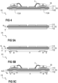
- a substrate includes a dielectric insulation layer, a first metallization layer attached to a first side of the dielectric insulation layer, and a second metallization layer attached to a second side of the dielectric insulation layer opposite the first side, wherein the second metallization layer includes one or more first areas and one or more second areas, wherein the second metallization layer in the one or more first areas has a first thickness, and in the one or more second areas has a second thickness that is greater than the first thickness.
- a method includes forming a first metallization layer on a first side of a dielectric insulation layer, and forming a second metallization layer on a second side of the dielectric insulation layer opposite the first side, wherein the second metallization layer includes one or more first areas and one or more second areas, wherein the second metallization layer in the one or more first areas has a first thickness, and in the one or more second areas has a second thickness that is greater than the first thickness.
- An electrical line or electrical connection as described herein may be a single electrically conductive element, or include at least two individual electrically conductive elements connected in series and/or parallel. Electrical lines and electrical connections may include metal and/or semiconductor material, and may be permanently electrically conductive (i.e., non-switchable).
- a semiconductor body as described herein may be made from (doped) semiconductor material and may be a semiconductor chip or be included in a semiconductor chip. A semiconductor body has electrically connecting pads and includes at least one semiconductor element with electrodes.
- the power semiconductor module arrangement 100 includes a housing 7 and a semiconductor substrate 10.
- the semiconductor substrate 10 includes a dielectric insulation layer 11, a (structured) first metallization layer 111 attached to the dielectric insulation layer 11, and a (structured) second metallization layer 112 attached to the dielectric insulation layer 11.
- the dielectric insulation layer 11 is disposed between the first and second metallization layers 111, 112.
- Each of the first and second metallization layers 111, 112 may consist of or include one of the following materials: copper; a copper alloy; aluminum; an aluminum alloy; any other metal or alloy that remains solid during the operation of the power semiconductor module arrangement.
- the semiconductor substrate 10 may be a ceramic substrate, that is, a substrate in which the dielectric insulation layer 11 is a ceramic, e.g., a thin ceramic layer.
- the ceramic may consist of or include one of the following materials: aluminum oxide; aluminum nitride; zirconium oxide; silicon nitride; boron nitride; or any other dielectric ceramic.
- the dielectric insulation layer 11 may consist of or include one of the following materials: Al 2 O 3 , AIN, SiC, BeO or Si 3 N 4 .
- the terminal elements 4 may consist of or include a metal such as copper, aluminum, gold, silver, or any alloys thereof, for example.
- the terminal elements 4 may be electrically and mechanically connected to the semiconductor substrate 10 by an electrically conductive connection layer (not specifically illustrated for the terminal elements 4).
- Such an electrically conductive connection layer generally may be a solder layer, a layer of an electrically conductive adhesive, or a layer of a sintered metal powder, e.g., a sintered silver powder, for example.
- terminal elements 4, instead of directly on the substrate 10, may alternatively or additionally be arranged on semiconductor bodies 20 or on any other metallic components of the power semiconductor module arrangement 100. That is, terminal elements 4 do not necessarily have to be connected to the first metallization layer 111 of the substrate 10.
Landscapes
- Chemical & Material Sciences (AREA)
- Engineering & Computer Science (AREA)
- Ceramic Engineering (AREA)
- Materials Engineering (AREA)
- Structural Engineering (AREA)
- Organic Chemistry (AREA)
- Microelectronics & Electronic Packaging (AREA)
- Cooling Or The Like Of Semiconductors Or Solid State Devices (AREA)
- Physics & Mathematics (AREA)
- Geometry (AREA)
Priority Applications (3)
| Application Number | Priority Date | Filing Date | Title |
|---|---|---|---|
| EP23218530.6A EP4576199A1 (fr) | 2023-12-20 | 2023-12-20 | Substrat et procédés de production d'un substrat |
| CN202411877380.7A CN120184108A (zh) | 2023-12-20 | 2024-12-19 | 衬底和用于制造衬底的方法 |
| US18/987,514 US20250210535A1 (en) | 2023-12-20 | 2024-12-19 | Substrate and methods for producing a substrate |
Applications Claiming Priority (1)
| Application Number | Priority Date | Filing Date | Title |
|---|---|---|---|
| EP23218530.6A EP4576199A1 (fr) | 2023-12-20 | 2023-12-20 | Substrat et procédés de production d'un substrat |
Publications (1)
| Publication Number | Publication Date |
|---|---|
| EP4576199A1 true EP4576199A1 (fr) | 2025-06-25 |
Family
ID=89224383
Family Applications (1)
| Application Number | Title | Priority Date | Filing Date |
|---|---|---|---|
| EP23218530.6A Pending EP4576199A1 (fr) | 2023-12-20 | 2023-12-20 | Substrat et procédés de production d'un substrat |
Country Status (3)
| Country | Link |
|---|---|
| US (1) | US20250210535A1 (fr) |
| EP (1) | EP4576199A1 (fr) |
| CN (1) | CN120184108A (fr) |
Citations (6)
| Publication number | Priority date | Publication date | Assignee | Title |
|---|---|---|---|---|
| EP0407905A2 (fr) * | 1989-07-08 | 1991-01-16 | DODUCO GMBH + Co Dr. Eugen DÀ¼rrwächter | Corps plan, en particulier pour l'application comme refroidisseur pour composants électroniques de puissance |
| US5672848A (en) * | 1993-12-28 | 1997-09-30 | Kabushiki Kaisha Toshiba | Ceramic circuit board |
| DE102012103786A1 (de) * | 2012-04-30 | 2013-10-31 | Curamik Electronics Gmbh | Metall-Keramik-Substrat sowie Verfahren zum Herstellen eines Metall-Keramik-Substrates |
| EP2449586B1 (fr) * | 2009-07-02 | 2020-10-21 | Rogers Germany GmbH | Dispositif électronique |
| DE102021100463A1 (de) * | 2021-01-13 | 2022-07-14 | Rogers Germany Gmbh | Verfahren zum Herstellen eines Metall-Keramik-Substrats und Metall-Keramik-Substrat hergestellt mit einem solchen Verfahren |
| DE102021125557A1 (de) * | 2021-10-01 | 2023-04-06 | Rogers Germany Gmbh | Metall-Keramik-Substrat und Verfahren zur Herstellung eines Metall-Keramik-Substrats |
-
2023
- 2023-12-20 EP EP23218530.6A patent/EP4576199A1/fr active Pending
-
2024
- 2024-12-19 US US18/987,514 patent/US20250210535A1/en active Pending
- 2024-12-19 CN CN202411877380.7A patent/CN120184108A/zh active Pending
Patent Citations (6)
| Publication number | Priority date | Publication date | Assignee | Title |
|---|---|---|---|---|
| EP0407905A2 (fr) * | 1989-07-08 | 1991-01-16 | DODUCO GMBH + Co Dr. Eugen DÀ¼rrwächter | Corps plan, en particulier pour l'application comme refroidisseur pour composants électroniques de puissance |
| US5672848A (en) * | 1993-12-28 | 1997-09-30 | Kabushiki Kaisha Toshiba | Ceramic circuit board |
| EP2449586B1 (fr) * | 2009-07-02 | 2020-10-21 | Rogers Germany GmbH | Dispositif électronique |
| DE102012103786A1 (de) * | 2012-04-30 | 2013-10-31 | Curamik Electronics Gmbh | Metall-Keramik-Substrat sowie Verfahren zum Herstellen eines Metall-Keramik-Substrates |
| DE102021100463A1 (de) * | 2021-01-13 | 2022-07-14 | Rogers Germany Gmbh | Verfahren zum Herstellen eines Metall-Keramik-Substrats und Metall-Keramik-Substrat hergestellt mit einem solchen Verfahren |
| DE102021125557A1 (de) * | 2021-10-01 | 2023-04-06 | Rogers Germany Gmbh | Metall-Keramik-Substrat und Verfahren zur Herstellung eines Metall-Keramik-Substrats |
Also Published As
| Publication number | Publication date |
|---|---|
| US20250210535A1 (en) | 2025-06-26 |
| CN120184108A (zh) | 2025-06-20 |
Similar Documents
| Publication | Publication Date | Title |
|---|---|---|
| EP3276657B1 (fr) | Refroidisseur, agencement d'un module semi-conducteur de puissance comportant un refroidisseur et procédé de production de celui-ci | |
| US20260101768A1 (en) | Base Plate for a Semiconductor Module Arrangement and Method for Producing a Base Plate | |
| CN109216234A (zh) | 用于处理半导体衬底的设备和方法 | |
| EP4084062A1 (fr) | Agencement de module d'alimentation à semi-conducteur | |
| US11935811B2 (en) | Baseplate for a semiconductor module and method for producing a baseplate | |
| EP4576199A1 (fr) | Substrat et procédés de production d'un substrat | |
| US20230369175A1 (en) | Power semiconductor module arrangement and method for producing the same | |
| CN110943057B (zh) | 功率半导体模块装置 | |
| EP4215508A1 (fr) | Substrat et procédé de fabrication d'un substrat | |
| EP4307359A1 (fr) | Agencement de module semi-conducteur de puissance et son procédé de fabrication | |
| EP4372807B1 (fr) | Agencement d'un substrat et procédés de production d'un agencement d'un substrat | |
| EP4607582A1 (fr) | Agencement de module semi-conducteur | |
| EP4601000A1 (fr) | Ensemble module semi-conducteur de puissance et son procédé de fabrication | |
| US20260094986A1 (en) | Rivet for use in semiconductor module arrangement and method for producing the same | |
| EP4270466A1 (fr) | Agencements de module semi-conducteur de puissance et procédés de production d'agencements de module semi-conducteur de puissance | |
| EP4428914A1 (fr) | Agencement de module semi-conducteur de puissance | |
| US20260090385A1 (en) | Semiconductor module comprising a housing | |
| EP4439649A1 (fr) | Agencement de substrat | |
| US20250275063A1 (en) | Method and system for connecting a terminal element to a substrate | |
| EP4651201A1 (fr) | Agencement de module semi-conducteur de puissance et ses procédés de fabrication | |
| US20260090317A1 (en) | System and method for mounting a housing to a base plate of a semiconductor module | |
| EP4510184A1 (fr) | Élément de borne et ensemble de modules semi-conducteurs de puissance comprenant un élément de borne | |
| EP3457434A1 (fr) | Substrat semi-conducteur pour un agencement de module semi-conducteur de puissance et son procédé de fabrication | |
| EP3951866A1 (fr) | Agencement de substrat semi-conducteur et son procédé de fabrication | |
| EP3889321B1 (fr) | Procédé de production d'un agencement de substrat à semiconducteur |
Legal Events
| Date | Code | Title | Description |
|---|---|---|---|
| PUAI | Public reference made under article 153(3) epc to a published international application that has entered the european phase |
Free format text: ORIGINAL CODE: 0009012 |
|
| STAA | Information on the status of an ep patent application or granted ep patent |
Free format text: STATUS: REQUEST FOR EXAMINATION WAS MADE |
|
| 17P | Request for examination filed |
Effective date: 20240918 |
|
| AK | Designated contracting states |
Kind code of ref document: A1 Designated state(s): AL AT BE BG CH CY CZ DE DK EE ES FI FR GB GR HR HU IE IS IT LI LT LU LV MC ME MK MT NL NO PL PT RO RS SE SI SK SM TR |