EP4576453A1 - Dispositif électro-optique à base de semi-conducteurs iii-v et/ou ii-vi et/ou du groupe iv et procédé - Google Patents
Dispositif électro-optique à base de semi-conducteurs iii-v et/ou ii-vi et/ou du groupe iv et procédé Download PDFInfo
- Publication number
- EP4576453A1 EP4576453A1 EP23219676.6A EP23219676A EP4576453A1 EP 4576453 A1 EP4576453 A1 EP 4576453A1 EP 23219676 A EP23219676 A EP 23219676A EP 4576453 A1 EP4576453 A1 EP 4576453A1
- Authority
- EP
- European Patent Office
- Prior art keywords
- doped
- region
- semiconductor material
- electro
- optical device
- Prior art date
- Legal status (The legal status is an assumption and is not a legal conclusion. Google has not performed a legal analysis and makes no representation as to the accuracy of the status listed.)
- Pending
Links
Images






Classifications
-
- G—PHYSICS
- G02—OPTICS
- G02F—OPTICAL DEVICES OR ARRANGEMENTS FOR THE CONTROL OF LIGHT BY MODIFICATION OF THE OPTICAL PROPERTIES OF THE MEDIA OF THE ELEMENTS INVOLVED THEREIN; NON-LINEAR OPTICS; FREQUENCY-CHANGING OF LIGHT; OPTICAL LOGIC ELEMENTS; OPTICAL ANALOGUE/DIGITAL CONVERTERS
- G02F1/00—Devices or arrangements for the control of the intensity, colour, phase, polarisation or direction of light arriving from an independent light source, e.g. switching, gating or modulating; Non-linear optics
- G02F1/01—Devices or arrangements for the control of the intensity, colour, phase, polarisation or direction of light arriving from an independent light source, e.g. switching, gating or modulating; Non-linear optics for the control of the intensity, phase, polarisation or colour
- G02F1/015—Devices or arrangements for the control of the intensity, colour, phase, polarisation or direction of light arriving from an independent light source, e.g. switching, gating or modulating; Non-linear optics for the control of the intensity, phase, polarisation or colour based on semiconductor elements having potential barriers, e.g. having a PN or PIN junction
- G02F1/017—Structures with periodic or quasi periodic potential variation, e.g. superlattices, quantum wells
- G02F1/01708—Structures with periodic or quasi periodic potential variation, e.g. superlattices, quantum wells in an optical wavequide structure
-
- H—ELECTRICITY
- H01—ELECTRIC ELEMENTS
- H01S—DEVICES USING THE PROCESS OF LIGHT AMPLIFICATION BY STIMULATED EMISSION OF RADIATION [LASER] TO AMPLIFY OR GENERATE LIGHT; DEVICES USING STIMULATED EMISSION OF ELECTROMAGNETIC RADIATION IN WAVE RANGES OTHER THAN OPTICAL
- H01S5/00—Semiconductor lasers
- H01S5/20—Structure or shape of the semiconductor body to guide the optical wave ; Confining structures perpendicular to the optical axis, e.g. index or gain guiding, stripe geometry, broad area lasers, gain tailoring, transverse or lateral reflectors, special cladding structures, MQW barrier reflection layers
- H01S5/22—Structure or shape of the semiconductor body to guide the optical wave ; Confining structures perpendicular to the optical axis, e.g. index or gain guiding, stripe geometry, broad area lasers, gain tailoring, transverse or lateral reflectors, special cladding structures, MQW barrier reflection layers having a ridge or stripe structure
-
- G—PHYSICS
- G02—OPTICS
- G02F—OPTICAL DEVICES OR ARRANGEMENTS FOR THE CONTROL OF LIGHT BY MODIFICATION OF THE OPTICAL PROPERTIES OF THE MEDIA OF THE ELEMENTS INVOLVED THEREIN; NON-LINEAR OPTICS; FREQUENCY-CHANGING OF LIGHT; OPTICAL LOGIC ELEMENTS; OPTICAL ANALOGUE/DIGITAL CONVERTERS
- G02F1/00—Devices or arrangements for the control of the intensity, colour, phase, polarisation or direction of light arriving from an independent light source, e.g. switching, gating or modulating; Non-linear optics
- G02F1/01—Devices or arrangements for the control of the intensity, colour, phase, polarisation or direction of light arriving from an independent light source, e.g. switching, gating or modulating; Non-linear optics for the control of the intensity, phase, polarisation or colour
- G02F1/015—Devices or arrangements for the control of the intensity, colour, phase, polarisation or direction of light arriving from an independent light source, e.g. switching, gating or modulating; Non-linear optics for the control of the intensity, phase, polarisation or colour based on semiconductor elements having potential barriers, e.g. having a PN or PIN junction
- G02F1/017—Structures with periodic or quasi periodic potential variation, e.g. superlattices, quantum wells
- G02F1/01783—Quantum wires
-
- G—PHYSICS
- G02—OPTICS
- G02F—OPTICAL DEVICES OR ARRANGEMENTS FOR THE CONTROL OF LIGHT BY MODIFICATION OF THE OPTICAL PROPERTIES OF THE MEDIA OF THE ELEMENTS INVOLVED THEREIN; NON-LINEAR OPTICS; FREQUENCY-CHANGING OF LIGHT; OPTICAL LOGIC ELEMENTS; OPTICAL ANALOGUE/DIGITAL CONVERTERS
- G02F1/00—Devices or arrangements for the control of the intensity, colour, phase, polarisation or direction of light arriving from an independent light source, e.g. switching, gating or modulating; Non-linear optics
- G02F1/01—Devices or arrangements for the control of the intensity, colour, phase, polarisation or direction of light arriving from an independent light source, e.g. switching, gating or modulating; Non-linear optics for the control of the intensity, phase, polarisation or colour
- G02F1/015—Devices or arrangements for the control of the intensity, colour, phase, polarisation or direction of light arriving from an independent light source, e.g. switching, gating or modulating; Non-linear optics for the control of the intensity, phase, polarisation or colour based on semiconductor elements having potential barriers, e.g. having a PN or PIN junction
- G02F1/017—Structures with periodic or quasi periodic potential variation, e.g. superlattices, quantum wells
- G02F1/01791—Quantum boxes or quantum dots
-
- H—ELECTRICITY
- H01—ELECTRIC ELEMENTS
- H01S—DEVICES USING THE PROCESS OF LIGHT AMPLIFICATION BY STIMULATED EMISSION OF RADIATION [LASER] TO AMPLIFY OR GENERATE LIGHT; DEVICES USING STIMULATED EMISSION OF ELECTROMAGNETIC RADIATION IN WAVE RANGES OTHER THAN OPTICAL
- H01S5/00—Semiconductor lasers
- H01S5/02—Structural details or components not essential to laser action
- H01S5/0206—Substrates, e.g. growth, shape, material, removal or bonding
- H01S5/021—Silicon based substrates
-
- H—ELECTRICITY
- H01—ELECTRIC ELEMENTS
- H01S—DEVICES USING THE PROCESS OF LIGHT AMPLIFICATION BY STIMULATED EMISSION OF RADIATION [LASER] TO AMPLIFY OR GENERATE LIGHT; DEVICES USING STIMULATED EMISSION OF ELECTROMAGNETIC RADIATION IN WAVE RANGES OTHER THAN OPTICAL
- H01S5/00—Semiconductor lasers
- H01S5/20—Structure or shape of the semiconductor body to guide the optical wave ; Confining structures perpendicular to the optical axis, e.g. index or gain guiding, stripe geometry, broad area lasers, gain tailoring, transverse or lateral reflectors, special cladding structures, MQW barrier reflection layers
- H01S5/2004—Confining in the direction perpendicular to the layer structure
-
- H—ELECTRICITY
- H01—ELECTRIC ELEMENTS
- H01S—DEVICES USING THE PROCESS OF LIGHT AMPLIFICATION BY STIMULATED EMISSION OF RADIATION [LASER] TO AMPLIFY OR GENERATE LIGHT; DEVICES USING STIMULATED EMISSION OF ELECTROMAGNETIC RADIATION IN WAVE RANGES OTHER THAN OPTICAL
- H01S5/00—Semiconductor lasers
- H01S5/20—Structure or shape of the semiconductor body to guide the optical wave ; Confining structures perpendicular to the optical axis, e.g. index or gain guiding, stripe geometry, broad area lasers, gain tailoring, transverse or lateral reflectors, special cladding structures, MQW barrier reflection layers
- H01S5/2054—Methods of obtaining the confinement
- H01S5/2077—Methods of obtaining the confinement using lateral bandgap control during growth, e.g. selective growth, mask induced
-
- H—ELECTRICITY
- H01—ELECTRIC ELEMENTS
- H01S—DEVICES USING THE PROCESS OF LIGHT AMPLIFICATION BY STIMULATED EMISSION OF RADIATION [LASER] TO AMPLIFY OR GENERATE LIGHT; DEVICES USING STIMULATED EMISSION OF ELECTROMAGNETIC RADIATION IN WAVE RANGES OTHER THAN OPTICAL
- H01S5/00—Semiconductor lasers
- H01S5/20—Structure or shape of the semiconductor body to guide the optical wave ; Confining structures perpendicular to the optical axis, e.g. index or gain guiding, stripe geometry, broad area lasers, gain tailoring, transverse or lateral reflectors, special cladding structures, MQW barrier reflection layers
- H01S5/22—Structure or shape of the semiconductor body to guide the optical wave ; Confining structures perpendicular to the optical axis, e.g. index or gain guiding, stripe geometry, broad area lasers, gain tailoring, transverse or lateral reflectors, special cladding structures, MQW barrier reflection layers having a ridge or stripe structure
- H01S5/2205—Structure or shape of the semiconductor body to guide the optical wave ; Confining structures perpendicular to the optical axis, e.g. index or gain guiding, stripe geometry, broad area lasers, gain tailoring, transverse or lateral reflectors, special cladding structures, MQW barrier reflection layers having a ridge or stripe structure comprising special burying or current confinement layers
- H01S5/2206—Structure or shape of the semiconductor body to guide the optical wave ; Confining structures perpendicular to the optical axis, e.g. index or gain guiding, stripe geometry, broad area lasers, gain tailoring, transverse or lateral reflectors, special cladding structures, MQW barrier reflection layers having a ridge or stripe structure comprising special burying or current confinement layers based on III-V materials
-
- G—PHYSICS
- G02—OPTICS
- G02F—OPTICAL DEVICES OR ARRANGEMENTS FOR THE CONTROL OF LIGHT BY MODIFICATION OF THE OPTICAL PROPERTIES OF THE MEDIA OF THE ELEMENTS INVOLVED THEREIN; NON-LINEAR OPTICS; FREQUENCY-CHANGING OF LIGHT; OPTICAL LOGIC ELEMENTS; OPTICAL ANALOGUE/DIGITAL CONVERTERS
- G02F2201/00—Constructional arrangements not provided for in groups G02F1/00 - G02F7/00
- G02F2201/06—Constructional arrangements not provided for in groups G02F1/00 - G02F7/00 integrated waveguide
- G02F2201/063—Constructional arrangements not provided for in groups G02F1/00 - G02F7/00 integrated waveguide ridge; rib; strip loaded
-
- G—PHYSICS
- G02—OPTICS
- G02F—OPTICAL DEVICES OR ARRANGEMENTS FOR THE CONTROL OF LIGHT BY MODIFICATION OF THE OPTICAL PROPERTIES OF THE MEDIA OF THE ELEMENTS INVOLVED THEREIN; NON-LINEAR OPTICS; FREQUENCY-CHANGING OF LIGHT; OPTICAL LOGIC ELEMENTS; OPTICAL ANALOGUE/DIGITAL CONVERTERS
- G02F2202/00—Materials and properties
- G02F2202/06—Materials and properties dopant
-
- G—PHYSICS
- G02—OPTICS
- G02F—OPTICAL DEVICES OR ARRANGEMENTS FOR THE CONTROL OF LIGHT BY MODIFICATION OF THE OPTICAL PROPERTIES OF THE MEDIA OF THE ELEMENTS INVOLVED THEREIN; NON-LINEAR OPTICS; FREQUENCY-CHANGING OF LIGHT; OPTICAL LOGIC ELEMENTS; OPTICAL ANALOGUE/DIGITAL CONVERTERS
- G02F2202/00—Materials and properties
- G02F2202/10—Materials and properties semiconductor
- G02F2202/101—Ga×As and alloy
-
- G—PHYSICS
- G02—OPTICS
- G02F—OPTICAL DEVICES OR ARRANGEMENTS FOR THE CONTROL OF LIGHT BY MODIFICATION OF THE OPTICAL PROPERTIES OF THE MEDIA OF THE ELEMENTS INVOLVED THEREIN; NON-LINEAR OPTICS; FREQUENCY-CHANGING OF LIGHT; OPTICAL LOGIC ELEMENTS; OPTICAL ANALOGUE/DIGITAL CONVERTERS
- G02F2202/00—Materials and properties
- G02F2202/10—Materials and properties semiconductor
- G02F2202/102—In×P and alloy
-
- H—ELECTRICITY
- H01—ELECTRIC ELEMENTS
- H01S—DEVICES USING THE PROCESS OF LIGHT AMPLIFICATION BY STIMULATED EMISSION OF RADIATION [LASER] TO AMPLIFY OR GENERATE LIGHT; DEVICES USING STIMULATED EMISSION OF ELECTROMAGNETIC RADIATION IN WAVE RANGES OTHER THAN OPTICAL
- H01S2304/00—Special growth methods for semiconductor lasers
-
- H—ELECTRICITY
- H01—ELECTRIC ELEMENTS
- H01S—DEVICES USING THE PROCESS OF LIGHT AMPLIFICATION BY STIMULATED EMISSION OF RADIATION [LASER] TO AMPLIFY OR GENERATE LIGHT; DEVICES USING STIMULATED EMISSION OF ELECTROMAGNETIC RADIATION IN WAVE RANGES OTHER THAN OPTICAL
- H01S5/00—Semiconductor lasers
- H01S5/04—Processes or apparatus for excitation, e.g. pumping, e.g. by electron beams
- H01S5/042—Electrical excitation ; Circuits therefor
- H01S5/0425—Electrodes, e.g. characterised by the structure
- H01S5/04254—Electrodes, e.g. characterised by the structure characterised by the shape
-
- H—ELECTRICITY
- H01—ELECTRIC ELEMENTS
- H01S—DEVICES USING THE PROCESS OF LIGHT AMPLIFICATION BY STIMULATED EMISSION OF RADIATION [LASER] TO AMPLIFY OR GENERATE LIGHT; DEVICES USING STIMULATED EMISSION OF ELECTROMAGNETIC RADIATION IN WAVE RANGES OTHER THAN OPTICAL
- H01S5/00—Semiconductor lasers
- H01S5/20—Structure or shape of the semiconductor body to guide the optical wave ; Confining structures perpendicular to the optical axis, e.g. index or gain guiding, stripe geometry, broad area lasers, gain tailoring, transverse or lateral reflectors, special cladding structures, MQW barrier reflection layers
- H01S5/22—Structure or shape of the semiconductor body to guide the optical wave ; Confining structures perpendicular to the optical axis, e.g. index or gain guiding, stripe geometry, broad area lasers, gain tailoring, transverse or lateral reflectors, special cladding structures, MQW barrier reflection layers having a ridge or stripe structure
- H01S5/2205—Structure or shape of the semiconductor body to guide the optical wave ; Confining structures perpendicular to the optical axis, e.g. index or gain guiding, stripe geometry, broad area lasers, gain tailoring, transverse or lateral reflectors, special cladding structures, MQW barrier reflection layers having a ridge or stripe structure comprising special burying or current confinement layers
- H01S5/2206—Structure or shape of the semiconductor body to guide the optical wave ; Confining structures perpendicular to the optical axis, e.g. index or gain guiding, stripe geometry, broad area lasers, gain tailoring, transverse or lateral reflectors, special cladding structures, MQW barrier reflection layers having a ridge or stripe structure comprising special burying or current confinement layers based on III-V materials
- H01S5/2209—GaInP based
-
- H—ELECTRICITY
- H01—ELECTRIC ELEMENTS
- H01S—DEVICES USING THE PROCESS OF LIGHT AMPLIFICATION BY STIMULATED EMISSION OF RADIATION [LASER] TO AMPLIFY OR GENERATE LIGHT; DEVICES USING STIMULATED EMISSION OF ELECTROMAGNETIC RADIATION IN WAVE RANGES OTHER THAN OPTICAL
- H01S5/00—Semiconductor lasers
- H01S5/30—Structure or shape of the active region; Materials used for the active region
- H01S5/34—Structure or shape of the active region; Materials used for the active region comprising quantum well or superlattice structures, e.g. single quantum well [SQW] lasers, multiple quantum well [MQW] lasers or graded index separate confinement heterostructure [GRINSCH] lasers
- H01S5/343—Structure or shape of the active region; Materials used for the active region comprising quantum well or superlattice structures, e.g. single quantum well [SQW] lasers, multiple quantum well [MQW] lasers or graded index separate confinement heterostructure [GRINSCH] lasers in AIIIBV compounds, e.g. AlGaAs-laser, InP-based laser
- H01S5/34313—Structure or shape of the active region; Materials used for the active region comprising quantum well or superlattice structures, e.g. single quantum well [SQW] lasers, multiple quantum well [MQW] lasers or graded index separate confinement heterostructure [GRINSCH] lasers in AIIIBV compounds, e.g. AlGaAs-laser, InP-based laser with a well layer having only As as V-compound, e.g. AlGaAs, InGaAs
Definitions
- the present invention provides an electro-optical device based on III-V and/or II-VI and/or group IV semiconductors and comprising a ridge structure.
- the invention also proposes a method for fabricating the electro-optical device.
- Semiconductor nano-ridge waveguides with a good current injection efficiency and/or limited non-radiative recombination, are used in monolithically integrated photonic devices.
- the electro-optical device includes a III-V semiconductor material ridge structure (e.g. GaAs), which is grown in a narrow Shallow Trench Isolation (STI) trench on a silicon (Si) V-groove formed in a Si support layer.
- III-V semiconductor material ridge structure e.g. GaAs
- STI Shallow Trench Isolation
- Si silicon
- the STI trench has a high aspect ratio (i.e. a ratio of its depth vs. its width is larger than at least 1), which has the advantage that misfits and dislocation defects are efficiently trapped (thus called aspect ratio trapping, ART) during the growth of the III-V semiconductor material inside the trench, and therefore the outgrown III-V semiconductor ridge material, i.e. a freestanding ridge structure, is free of defects.
- ART aspect ratio trapping
- the nano-ridge shape on top of the STI trenches can be engineered and manipulated by the applied growth conditions, hence, this ridge integration approach is called NRE.
- the support layer is highly n-doped, (i.e., doped with n-type impurities) and the ridge structure itself comprises an n-doped III-V semiconductor material (e.g. GaAs) region arranged near the bottom of the ridge structure and contacting the n-doped support layer in the trench.
- n-doped III-V semiconductor material e.g. GaAs
- the ridge structure comprises a III-V semiconductor material (e.g. GaAs) region arranged in the center of the ridge structure that is unintentionally doped (also referred to as non-intentionally doped or NID), and containing an active region.
- the ridge structure also comprises a p-doped III-V semiconductor material (e.g. GaAs) region arranged at the top of the ridge structure that is in contact with a metallic interface.
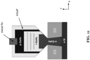
- the ridge structure has a substantially rectangular shape, in particular in the top or upper region (that is, the region opposite to the Si support layer in the exemplary coordinate system depicted in FIG. 11 ).
- the ridge structure comprises a capping layer of a higher band-gap III-V material with respect to the preceding layer (e.g. InGaP, lattice matched to e.g. the GaAs of the ridge structure) grown around the III-V semiconductor material ridge structure, particularly around a wider portion thereof.
- the capping layer has a conduction and/or valence band offset, which is sufficiently high to prevent at least one species of charge carriers (i.e. electrons and/or holes) to penetrate into the capping layer and to reach its surface interface with a dielectric, which encapsulates the ridge structure and the capping layer.
- the ridge structure according to FIG. 11 includes a region near the top of the ridge structure where III-V semiconductor material was removed by etching, in order to form a narrower top portion referred to as metal fin or metal fin structure.
- the purpose of the metal fin structure is to inject carriers into the active region of the ridge structure, in operation of the electro-optical device.
- the optical waveguide mode is not pushed downwards but has a strong overlap with the metal fin and the metal-semiconductor interface mentioned above. This overlap causes very strong optical absorption and hinders, e.g., laser operation.
- the metal fin can be replaced by a largely spaced plug array to reduce the optical losses in the metal region. Consequently, the current density in each metal plug must be very high to ensure sufficient current injection to the active region. This, in turn, will cause new problems such as defect formation in the semiconductor close to the metal fin and along the interface, resulting in laser device failure.
- embodiments of the present invention aim to provide an improved electro-optical device.
- An objective is to provide an electro-optical device with a ridge structure that shows better contact design properties.
- Another objective is to reduce surface recombination by preventing exposure of relevant semiconductor material regions, in order to maximize charge carrier densities in the active region of the electro-optical device, and to reduce optical losses of light being waveguided in the ridge.
- the embodiments are based on the following considerations.
- the n-doped layer is arranged on the bottom of the ridge structure, and the p-doped layer is arranged on the top of the ridge structure. This means that electrons are injected into the ridge structure from the bottom and holes are injected from the ridge structure from the top.
- the embodiments of the present invention are based on the idea of providing a trapezoid-shaped region of the semiconductor ridge structure (made e.g. by GaAs) that encapsulates the active region and is anisotropically capped with another semiconductor material (e.g. InGaP), which, importantly, covers little to no GaAs on the top narrower part of the trapezoid-shaped region.
- the design of the ridge structure provides a continuous electrical contact to the active region, wherein the contact may employ a semiconductor fin structure placed on top of the trapezoid-shaped region and a continuous metal ridge or an array of metal plugs placed on top of the fin structure.
- a first aspect of the invention provides an electro-optical device based on III-V and/or II-VI and/or group IV semiconductors, comprising a support region and a ridge structure extending from the support region.
- the ridge structure comprises: a bottom region comprising at least one layer of a first semiconductor material, the first semiconductor material having a first impurity type, the bottom region being provided on the support region; an intermediate region comprising at least one layer of a second semiconductor material, the intermediate region being provided on the bottom region and comprising an active region, wherein the intermediate region has a trapezoid-shaped top region with a top surface, side surfaces, and inclined surfaces that connect the top surface to the side surfaces; a capping layer comprising at least one layer of a third semiconductor material, the capping layer being provided on the side surfaces and the inclined surfaces of the intermediate region, wherein the third semiconductor material has a higher band-gap than the second semiconductor material; and a fin structure comprising at least one layer of a fourth semiconductor material having a second impurity type
- a layer/region provided on top of another layer/region may cover any exposed surface of the region/layer below only partly or completely. Also, a thickness of the layer/region on the surface of the region/layer below it can be controlled, particularly relative to the thickness of the layer/region on the other surfaces of the region/layer beneath it.
- the terms “upwards”, “top”, “above” etc. relate to the terms “downwards”, “bottom”, “below” etc. according to a fabrication direction, e.g. by epitaxial growth, of the electro-optical device. That is, the "lowest” point of the ridge structure is on the support region, and the support region is “below” the ridge structure.
- the ridge structure extends “upwards” from the support region, and the fin structure is provided “on top” and “above” the ridge structure.
- the "first conductivity type” may be an n-type or p-type, and a “second-conductivity-type” may accordingly be a p-type or n-type.
- first-conductivity-type charge carriers maybe electrons or holes, and “second-conductivity-type charge carriers” may accordingly be holes or electrons.
- the design utilizes a continuous contact ridge by forming the semiconductor fin structure on the top surface of the trapezoid-shaped top region of the intermediate region, thereby enabling the electro-optical device, when in operation, to confine current injection, pull down the optical mode to reduce optical losses, increase the separation from the metal/semiconductor interface to the optical gain region to reduce non-radiative carrier recombination and defect formation, and hence, prevent excessive current and temperature gradients, which may lead to device failure.
- one or more metal plugs are further arranged on the fin structure.
- the electro-optical device can be processed in one epitaxial growth step and no regrowth is needed. Moreover, integration of the electro-optical device is simplified, resulting in reduced costs.
- the top surface of the intermediate region comprises a ⁇ 001 ⁇ surface of the second semiconductor material.
- the inclined surfaces of the intermediate region comprise ⁇ 111 ⁇ surfaces of the second semiconductor material.
- the fin structure is provided directly on the top surface of the intermediate region.
- the capping layer is further provided on the top surface of the intermediate region; and the fin structure is provided directly on the capping layer on the top surface of the intermediate region.
- a width of the fin structure is narrower than a width of the capping layer.
- the electro-optical device further comprises an electrode electrically contacting a top surface of the fin structure and configured to inject second-conductivity-type charge carriers into the ridge structure through the fin structure.
- the bottom region of the ridge structure is narrower than the intermediate region of the ridge structure.
- the active region comprises one or more quantum wells and/or one or more quantum dots and/or one or more quantum wires and/or a bulk material.
- the first semiconductor material comprises at least one of: doped GaAs, doped InP, doped InAs, doped GaSb, doped InGaAs, doped InGaAsSb, or doped, or doped GaAlAs.
- the second semiconductor material comprises at least one of: unintentionally doped or doped GaAs, unintentionally doped or doped InP, unintentionally doped or doped InAs, unintentionally doped or doped GaSb, unintentionally doped or doped InGaAs, unintentionally doped or doped InGaAsSb, or unintentionally doped or doped InGaAsP, or unintentionally doped or doped InGaAsN.
- the third semiconductor material comprises at least one of: unintentionally doped or doped AlAsSb, unintentionally doped or doped InGaP, unintentionally doped or doped AlGaSb, unintentionally doped or doped GaAlPSb, or unintentionally doped or doped InAlAs, or unintentionally doped or doped GaAlAs.
- the fourth semiconductor material comprises at least one of: doped GaAs, doped InP, doped InAs, doped GaSb, doped InGaAs, doped InGaAsSb, or doped GaAlAs
- the electro-optical device is a laser, a light emitting diode (LED), an optical amplifier, a single photon source, an optical modulator, a saturable absorber, or an optical detector.
- LED light emitting diode
- the electro-optical device is a laser, a light emitting diode (LED), an optical amplifier, a single photon source, an optical modulator, a saturable absorber, or an optical detector.
- a second aspect of the invention provides a method for fabricating an electro-optical device based on III-V and/or II-VI and/or group IV semiconductors.
- the method comprises providing a support region; and growing a ridge structure extending from the support region by: growing a bottom region onto the support region, the bottom region comprising at least one layer of a first semiconductor material having a first conductivity type; growing an intermediate region onto the bottom region, the intermediate region comprising an active region, and the intermediate region comprising at least one layer of a second semiconductor material, wherein the intermediate region has a trapezoid-shaped top region with a top surface, side surfaces, and inclined surfaces that connect the top surface to the side surfaces; growing a capping layer onto the side surfaces and the inclined surfaces of the intermediate region, the capping layer comprising at least one layer of a third semiconductor material, wherein the third semiconductor material has a higher band-gap than the second semiconductor material; and forming a fin structure onto the top region of the intermediate region, the fin structure comprising at least one layer
- the top surface of the intermediate region comprises a ⁇ 001 ⁇ surface of the second semiconductor material.
- the inclined surfaces of the intermediate region comprise ⁇ 111 ⁇ surfaces of the second semiconductor material.
- the method further comprises forming the fin structure directly on the top surface of the intermediate region.
- the method further comprises growing the capping layer onto the top surface of the intermediate region; and forming the fin structure directly on the capping layer on the top surface of the intermediate region.
- the method further comprises forming a transition layer between the top surface of the intermediate region and the capping layer.
- a width of the fin structure is narrower than a width of the capping layer.
- the method further comprises depositing an electrode electrically contacting a top surface of the fin structure and configured to inject second-conductivity-type charge carriers into the ridge structure through the fin structure.
- the bottom region of the ridge structure is narrower than the intermediate region of the ridge structure.
- the active region comprises one or more quantum wells and/or one or more quantum dots and/or one or more quantum wires and/or a bulk material.
- the first semiconductor material comprises at least one of: doped GaAs, doped InP, doped InAs, doped GaSb, doped InGaAs, doped InGaAsSb, or doped, or doped GaAlAs
- the second semiconductor material comprises at least one of: unintentionally doped or doped GaAs, unintentionally doped or doped InP, unintentionally doped or doped InAs, unintentionally doped or doped GaSb, unintentionally doped or doped InGaAs, unintentionally doped or doped InGaAsSb, or unintentionally doped or doped InGaAsP, or unintentionally doped or doped InGaAsN.
- the third semiconductor material comprises at least one of: unintentionally doped or doped AlAsSb, unintentionally doped or doped InGaP, unintentionally doped or doped AlGaSb, unintentionally doped or doped GaAlPSb, or unintentionally doped or doped InAlAs, or unintentionally doped or doped GaAlAs.
- the fourth semiconductor material comprises at least one of: doped GaAs, doped InP, doped InAs, doped GaSb, doped InGaAs, doped InGaAsSb, or doped GaAlAs.
- the method of the second aspect achieves the same advantages as the device of the first aspect and maybe extended by respective implementations as described above for the device of the first aspect.
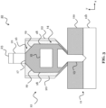
- FIG. 1 shows a cross-section of an exemplary embodiment of an electro-optical device 10 according to the invention.
- the device 10 is a monolithically integrated electro-optical device, and is based on III-V semiconductors and/or II-VI semiconductors and/or group IV semiconductors.
- the electro-optical device 10 may be a laser, a LED, an optical amplifier, a single photon source, an optical modulator, a saturable absorber, or an optical detector.
- the electro-optical device 10 may be fabricated using the so-called nano-ridge engineering (NRE) approach.
- the electro-optical device 10 comprises a support region 11.
- the support region 11 may comprise a substrate made of Si, or Ge, or SiC, or any binary III-V material or any binary II-IV material.
- the support region 11 may comprise a narrow STI trench 11a on a V-groove formed in a semiconductor-material substrate 11b.
- the support region 11 may be an engineered substrate realized by bonding a crystalline seed layer to a handling substrate and processing a trench-pattern, as the one depicted in FIG. 1 .
- the engineered substrate may provide a crystalline surface for epitaxial deposition of the other parts of the electro-optical device 10.
- the electro-optical device 10 further comprises a ridge structure 12 extending from the support region 11.
- the ridge structure 12 may be fabricated using the NRE approach on the support region 11, i.e. may be grown in a high-aspect-ratio trench that is formed before in the support region 11.
- the ridge structure 12 may extend on the support region 11 along a direction, which is into the plane depicted in the cross-section shown in FIG. 1 , where a reference coordinate system is depicted.
- the ridge structure 12 includes a plurality of different regions and layers. Namely, the ridge structure 12 includes a bottom region 13, which is provided on the support region 11. The bottom region 13 comprises at least one layer of a first semiconductor material, the first semiconductor material having a first impurity type.
- the bottom region 13 may be grown in the high-aspect ratio trench mentioned above.
- the bottom region 13, thus, may be narrower compared to a maximum width of the ridge structure 12.
- the ridge structure 12 further comprises an intermediate region 14 provided on the bottom region 13 and comprises an active region 15.
- the intermediate region 14 comprises, or is made of, at least one layer of a second semiconductor material.
- the active region 15 can emit or absorb or modulate light, and may comprise at least one layer comprising one or more quantum wells and/or one or more quantum dots and/or one or more quantum wires and/or a bulk material.
- the intermediate region 14 is formed so that it has a trapezoid-shaped top region 16. That is, the top region 16 (or upper part) of the intermediate region 14 has two side surfaces 18, a top surface 17 and two inclined surfaces 19 that connect the top surface 17 to the side surfaces 18. In this manner, the intermediate region 14 has an upper part which, in the plane of the cross-section shown in FIG. 1 , has the shape of a trapezoid, where the top surface 17 has a width (in the x axis depicted in the coordinate system of FIG. 1 ) that is smaller than a total width of the intermediate region 14.
- the total width of the intermediate region 14 may be determined, for example, as being a distance between the two side surfaces 18 (in the x-direction in the coordinate system depicted in FIG. 1 ).
- the top region 16 of the intermediate region 14 may have a truncated-pyramidal shape.
- the top surface 17 of the intermediate region 14 may comprise a ⁇ 001 ⁇ surface of the second semiconductor material, and the inclined surfaces 19 may comprise each a ⁇ 111 ⁇ surface of the second semiconductor material.
- the side surfaces 18 may comprise each a ⁇ 110 ⁇ surface of the second semiconductor material.
- the lower part of the intermediate region 14 may have an inverted trapezoid-shape, compared to the trapezoid defined in the upper part (or top region 16), as depicted in the embodiment according to FIG. 1 , with two lower inclined surfaces and a bottom surface, where the lower inclined surfaces connect the bottom surface to the two side surfaces 18.
- the lower part of the intermediate region 14 may have any other shape.
- it may have a rectangular or squared shape (in two dimensions or 2D, and it has then a rectangular-box shape or cubic-box shape, respectively, in 3D). This is not limited in this disclosure.
- FIG. 2a - d show four examples for the intermediate region 14, each having a trapezoid shape.
- the top surface 17 of the intermediate region 14 shown in FIG. 2a ) and FIG. 2d ) have a width larger than the top surface 17 of the intermediate region 14 shown in FIG. 2b ).
- the top surface 17 of the intermediate region 14 shown in FIG. 2 c) highlights the absence of any capping layer, as will be explained later on in this document.
- Same elements in FIG. 1 and FIG. 2a )-d) share the same reference signs and function likewise.
- the ridge structure 12 further comprises a capping layer 20 that is provided on the side surfaces 18 and the inclined surfaces 19 of the intermediate region 14.
- the capping layer comprises at least one layer of a third semiconductor material, wherein the third semiconductor material has a higher band-gap than the second semiconductor material.
- the ⁇ 001 ⁇ facet of the second semiconductor material of the intermediate layer 14 is not covered by the capping layer, i.e. remains exposed.
- the ridge structure 12 further comprises a fin structure 21 that comprises, or is made of, at least one layer of a fourth semiconductor material, the fourth semiconductor material having a second impurity type.
- the fin structure 21 extends upwards from the top region 16 of the intermediate region 14.
- One or more metal plugs or metal structures may be arranged on the fin structure 21 (not shown).
- the fin structure 21 is thus provided directly on the top surface 17 of the intermediate region 14, thereby allowing a good carrier injection into the active region whilst maintaining sufficient surface passivation and good carrier confinement.
- a width of the fin structure 21 is narrower than a width of the capping layer 20
- the bottom region 13 may be narrower compared to the maximum width of the ridge structure 12. That is, the bottom region 13 may be narrower compared to the total width of the intermediate region 14 and a width of the capping layer 20 provided on each of the side surfaces 18 of the intermediate region 14. Accordingly, the bottom region 13 may be narrower compared to the total width of the intermediate region 14.
- the first semiconductor material may comprise at least one of: doped GaAs, doped InP, doped InAs, doped GaSb, doped InGaAs, doped InGaAsSb, or doped, or doped GaAlAs.
- the second semiconductor material of the intermediate region 14 may comprise at least one of: unintentionally doped or doped GaAs, unintentionally doped or doped InP, unintentionally doped or doped InAs, unintentionally doped or doped GaSb, unintentionally doped or doped InGaAs, unintentionally doped or doped InGaAsSb, or unintentionally doped or doped InGaAsP, or unintentionally doped or doped InGaAsN.
- the third semiconductor material of the capping layer 20 may comprise at least one of: unintentionally doped or doped AlAsSb, unintentionally doped or doped InGaP, unintentionally doped or doped AlGaSb, unintentionally doped or doped GaPSb, or unintentionally doped or doped InAlAs, or unintentionally doped or doped GaAlAs.
- the fourth semiconductor material of the fin structure 21 may comprise at least one of: doped GaAs, doped InP, doped InAs, doped GaSb, doped InGaAs, doped InGaAsSb, or doped, or unintentionally doped or doped GaAlAs.
- the electro-optical device 10 maybe a laser, a LED, an optical amplifier, a single photon source, an optical modulator, a saturable absorber, or an optical detector.
- a choice of the first semiconductor material, the second semiconductor material, the third semiconductor material and the fourth semiconductor material depend on the desired implementation/usage of the electro-optical device 10 and may be defined to ensure good wave guidance for the relevant wavelength required for the respective device implementation/usage.
- Exemplary materials used for the ridge structure 12 so that the electro-optical device 10 is, for example and not as a limitation, a GaAs Laser, a InGaAs Laser, and InP Laser, or a GaSb laser are shown in Table I. Table I. Examples for the semiconductor materials used in possible lasers based on the electro-optical device 10.
- the respective dimension of the bottom region 13, the intermediate region 14, the capping layer 20 and the fin structure 21 may vary depending on the desired use of the electro-optical device 10 and, thus, on the employed semiconductor materials.
- a width of the fin structure 21 may be larger than 5 nanometers (nm) and smaller than a largest width at which the fin structure 21 does not guide waves of the respective material.
- An upper limit for the width of the fin structure 21 for the GaAs/InGaAs Laser is ⁇ 250 nm.
- a width of the top surface 17 of the intermediate region 14 may be larger or smaller than the width of the fin structure 21 and smaller than the maximum width of the intermediate region 14. Further, a width of the capping layer 20 that is provided on the side surfaces 18 and on the inclined surfaces 19 of the intermediate region 14 may be above 10 nm.
- FIG. 3 shows a cross-section of an exemplary embodiment of an electro-optical device 10 according to the invention, which builds on the electro-optical device 10 shown in FIG. 1 . Same elements share the same reference signs and function likewise. Hereinafter, only the differences between FIG. 1 and FIG. 3 are explained.
- the electro-optical device 10 in particular the ridge structure 12, further comprises an electrode 23 electrically contacting a top surface of the fin structure 21.
- the first-conductivity-type may be n-type and the second-conductivity-type may be p-type.
- First-conductivity-type charge carriers are thus electrons, and second-conductivity-type charge carriers are holes. However, these polarities can also be exchanged.
- the fin structure 21 enables the electro-optical device 10 to confine current injection, pull down the optical mode to reduce optical losses, increase a separation from the metal/semiconductor interface to the optical active region 15, and prevent excessive current and temperature gradients.
- FIG. 4 shows an example of a 3D view of the electro-optical device 10 according to the embodiment of FIG. 3 . Same elements in FIG. 3 and FIG. 4 share the same reference signs and function likewise.
- the fin structure 21 may further comprise a second layer 21b that maybe made of the fourth semiconductor material having the second impurity type to ensure low contact resistance.
- Exemplary simulation results for a mode profile and for an absorption region obtained for the electro-optical device 10 according to the embodiment shown in FIG. 3 and FIG. 4 are shown respectively in FIG. 5a) and FIG. 5b ).
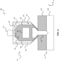
- FIG. 6 shows a cross-section of another exemplary embodiment of an electro-optical device 10 according to the invention, which builds on the electro-optical device 10 shown in FIG. 1 . Same elements share the same reference signs and function likewise. Hereinafter, only the differences between FIG. 1 and FIG. 6 are explained.
- the capping layer 20 is further provided on the top surface 17 of the intermediate region 14. That is, the capping layer 20 covers at least partially or totally the ⁇ 001 ⁇ facet of the top surface 17 of the intermediate region 14.
- the ridge structure 12 in this exemplary embodiment may further comprise a transition layer 24 that is provided between the top surface 17 of the intermediate region 14 and the capping layer 20 on top of it.
- the transition layer 24 may also be unintentionally provided on the inclined surfaces (19) of the intermediate region 14 (not shown) and/or on the side surfaces (18) of the intermediate region 14 (not shown).
- the transition layer 24 may comprise, or may be formed of, at least one layer of a fifth semiconductor material.
- the fifth semiconductor material may comprise the second semiconductor material being doped with first conductivity-type impurities or with second conductivity-type impurities.
- the transition layer 24 may comprise n-doped or p-doped GaAs.
- the fin structure 21 is provided directly on the capping layer 20 that is provided on the top surface 17 of the intermediate region 14.
- FIG. 7 shows a cross-section of another exemplary embodiment of an electro-optical device 10 according to the invention, which builds on the electro-optical device 10 shown in FIG. 6 . Same elements share the same reference signs and function likewise. Hereinafter, only the differences between FIG. 6 and FIG. 7 are explained.
- the electro-optical device 10 in particular the ridge structure 12, further comprises an electrode 23 electrically contacting a top surface of the fin structure 21.
- the electrode 23 is configured to inject second-conductivity-type charge carriers into the ridge structure 12, in particular into the intermediate region 14, through the fin structure 21 and through the transition layer 24.
- the electrode 23 may comprise, or may be made of, a metallic material.
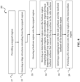
- FIG. 8 shows schematically a method 30 for fabricating the electro-optical device 10, according to an embodiment of the invention.
- the method 30 includes at least the following steps: A step 31 of providing a support region 11, and a step 32 of growing a ridge structure 12 extending from the support region 11.
- the step 32 may comprise: A step 33 of growing a bottom region 13 onto the support region 11, the bottom region 13 comprising at least one layer of a first semiconductor material having a first conductivity type; and a step 34 of growing an intermediate region 14 onto the bottom region 13, the intermediate region 14 comprising an active region 15, and the intermediate region 14 comprising at least one layer of a second semiconductor material, wherein the intermediate region 14 has a trapezoid-shaped top region 16 with a top surface 17, side surfaces 18, and inclined surfaces 19 that connect the top surface 17 to the side surfaces 18.
- the step 32 may further comprise a step 35 growing a capping layer 20 onto the side surfaces 18 and the inclined surfaces 19 of the intermediate region 14, the capping layer 20 comprising at least one layer of a third semiconductor material, and wherein the third semiconductor material has a higher band-gap than the second semiconductor material.
- the step 32 may comprise a step 36 of forming a fin structure 21 onto the top region 16 of the intermediate region 14, the fin structure 21 comprising a fourth semiconductor material having a second conductivity type.
- a STI trench 11a may be formed in the support region 11, and the ridge structure 12 may be epitaxially grown in the STI trench 11a.
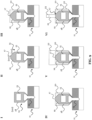
- FIG. 9 schematically depicts exemplary steps for the method 32 above.
- the bottom region 13 can be grown onto the support region 11.
- a lower part of the intermediate region 14 may be grown onto the bottom region 13, and may be made of the second semiconductor material.
- This lower part has a substantially rectangular shape.
- the side surfaces 18 of the intermediate region 14 may comprise ⁇ 110 ⁇ surfaces.
- the active region 15 may also be formed in the intermediate region 14.
- the trapezoid-shaped top region 16 of the intermediate region 14 maybe formed by using a facet growth rate manipulation technique, which is called NRE. That is, the two inclined surfaces 19 may be formed comprising ⁇ 111 ⁇ surfaces of the second semiconductor material, and the top surface 17 of the intermediate region 14 maybe formed, comprising a ⁇ 001 ⁇ surface of the second semiconductor material, with the inclined surfaces 19 connecting the top surface 17 to the side surfaces 18.
- NRE facet growth rate manipulation technique
- the capping layer 20 comprising the at least one layer of the third semiconductor material, may be grown onto the side surfaces 18, the inclined surfaces 19 and the top surface 17 of the intermediate region 14.
- the capping layer 20 onto the top surface 17 may be removed in situ (e.g., via annealing or etching within a same growth chamber), in step IV, so that the top surface 17 is exposed.
- the fin structure 21 is formed by growing at least one layer 22 of the fourth semiconductor material onto the intermediate structure 14 and the capping layer 20.
- the at least one layer 22 maybe subsequently etched to form the fin structure 21 only onto the top surface 17 of the intermediate layer 14.
- the electrode 23 may also be formed.
- FIG. 10 schematically depicts an exemplary method for the case where the capping layer 20 is still present on the top surface 17 of the intermediate region 14.
- Step I according to FIG. 10 depicts that the at least one layer 22 may be grown before removing the capping layer 20.
- step II there may be still a part of the capping layer 20 provided onto the top surface 17 of the intermediate layer 14.
- the capping layer 20 maybe n-doped or p-doped.
- the transition layer 24 may be formed between the top surface 17 of the intermediate region 14 and the capping layer 20 directly on top of it.
- the transition layer 24 may be formed by doping totally or partially the second semiconductor material of the top surface 17 of the trapezoid-shaped top region 16. This is indicated in step IV in FIG. 10 .
Landscapes
- Physics & Mathematics (AREA)
- General Physics & Mathematics (AREA)
- Optics & Photonics (AREA)
- Nonlinear Science (AREA)
- Condensed Matter Physics & Semiconductors (AREA)
- Electromagnetism (AREA)
- Geometry (AREA)
- Semiconductor Lasers (AREA)
Priority Applications (3)
| Application Number | Priority Date | Filing Date | Title |
|---|---|---|---|
| EP23219676.6A EP4576453A1 (fr) | 2023-12-22 | 2023-12-22 | Dispositif électro-optique à base de semi-conducteurs iii-v et/ou ii-vi et/ou du groupe iv et procédé |
| CN202411878798.XA CN120200097A (zh) | 2023-12-22 | 2024-12-19 | 基于iii-v和/或ii-vi和/或iv族半导体的电光器件及方法 |
| US18/989,974 US20250208444A1 (en) | 2023-12-22 | 2024-12-20 | Electro-optical devices having ridge semiconductor structure and methods of fabricating the same |
Applications Claiming Priority (1)
| Application Number | Priority Date | Filing Date | Title |
|---|---|---|---|
| EP23219676.6A EP4576453A1 (fr) | 2023-12-22 | 2023-12-22 | Dispositif électro-optique à base de semi-conducteurs iii-v et/ou ii-vi et/ou du groupe iv et procédé |
Publications (1)
| Publication Number | Publication Date |
|---|---|
| EP4576453A1 true EP4576453A1 (fr) | 2025-06-25 |
Family
ID=89430503
Family Applications (1)
| Application Number | Title | Priority Date | Filing Date |
|---|---|---|---|
| EP23219676.6A Pending EP4576453A1 (fr) | 2023-12-22 | 2023-12-22 | Dispositif électro-optique à base de semi-conducteurs iii-v et/ou ii-vi et/ou du groupe iv et procédé |
Country Status (3)
| Country | Link |
|---|---|
| US (1) | US20250208444A1 (fr) |
| EP (1) | EP4576453A1 (fr) |
| CN (1) | CN120200097A (fr) |
Citations (2)
| Publication number | Priority date | Publication date | Assignee | Title |
|---|---|---|---|---|
| EP3506000A1 (fr) * | 2017-12-29 | 2019-07-03 | IMEC vzw | Structure de guide d'onde semi-conducteur iii-v nanoridge |
| EP3671982A1 (fr) * | 2018-12-21 | 2020-06-24 | IMEC vzw | Dispositif opto-électronique à nanocrête iii-v-sur-silicium doté d'une structure d'ailette formée par recroissance |
-
2023
- 2023-12-22 EP EP23219676.6A patent/EP4576453A1/fr active Pending
-
2024
- 2024-12-19 CN CN202411878798.XA patent/CN120200097A/zh active Pending
- 2024-12-20 US US18/989,974 patent/US20250208444A1/en active Pending
Patent Citations (2)
| Publication number | Priority date | Publication date | Assignee | Title |
|---|---|---|---|---|
| EP3506000A1 (fr) * | 2017-12-29 | 2019-07-03 | IMEC vzw | Structure de guide d'onde semi-conducteur iii-v nanoridge |
| EP3671982A1 (fr) * | 2018-12-21 | 2020-06-24 | IMEC vzw | Dispositif opto-électronique à nanocrête iii-v-sur-silicium doté d'une structure d'ailette formée par recroissance |
Non-Patent Citations (1)
| Title |
|---|
| "Future directions in silicon photonics; IN: SEMICONDUCTORS AND SEMIMETALS; ISSN 0080-8784", vol. 101, 1 January 2019, ACADEMIC PRESS, SAN DIEGO, CA., US, ISBN: 978-0-12-818857-6, ISSN: 0080-8784, article VAN THOURHOUT DRIES ET AL: "Nano-ridge laser monolithically grown on (001) Si", pages: 283 - 304, XP055808730, DOI: 10.1016/bs.semsem.2019.07.002 * |
Also Published As
| Publication number | Publication date |
|---|---|
| CN120200097A (zh) | 2025-06-24 |
| US20250208444A1 (en) | 2025-06-26 |
Similar Documents
| Publication | Publication Date | Title |
|---|---|---|
| CN102292833B (zh) | Iii-v族化合物半导体受光元件 | |
| CN1973378A (zh) | 长波长vcsel的隧道结 | |
| US20190296131A1 (en) | Method of Manufacture of Germanium-Silicon-Tin Heterojunction Bipolar Transistor Devices | |
| US7701993B2 (en) | Semiconductor optical device and a method of fabricating the same | |
| US7295586B2 (en) | Carbon doped GaAsSb suitable for use in tunnel junctions of long-wavelength VCSELs | |
| WO2021055599A1 (fr) | Procédés d'injection de trous dans des diodes électroluminescentes au nitrure de gallium-aluminium-indium | |
| US12366704B1 (en) | Photonic integrated chip structure and fabrication method thereof | |
| JP4664725B2 (ja) | 半導体レーザ素子 | |
| EP4576453A1 (fr) | Dispositif électro-optique à base de semi-conducteurs iii-v et/ou ii-vi et/ou du groupe iv et procédé | |
| US7986721B2 (en) | Semiconductor optical device including a PN junction formed by a second region of a first conductive type semiconductor layer and a second conductive type single semiconductor layer | |
| US20200203930A1 (en) | Iii-v-on-silicon nanoridge opto-electronic device with a regrown fin structure | |
| CN116231451B (zh) | 垂直腔面发射激光器的制备方法及垂直腔面发射激光器 | |
| US12278464B2 (en) | Edge emitting laser device | |
| Hara et al. | Self-organised InGaAs quantum wire lasers on GaAs multi-atomic steps | |
| JP2001203423A (ja) | 半導体発光装置 | |
| JP2001185809A (ja) | 半導体光デバイス装置及びその製造方法 | |
| JP2020098891A (ja) | 半導体レーザ | |
| US7838893B2 (en) | Semiconductor optical device | |
| US7208774B2 (en) | Semiconductor optical device | |
| US20030119222A1 (en) | Hybrid confinement layers of buried heterostructure semiconductor laser | |
| JP3421836B2 (ja) | 半導体装置の製造方法 | |
| US20060243992A1 (en) | Semiconductor light-emitting device | |
| JP2002252406A (ja) | 埋め込みリボン半導体レーザと製造方法 | |
| US20200203929A1 (en) | Iii-v-on-silicon nanoridge opto-electronic device with carrier blocking layers | |
| CN120836124A (zh) | 表面发射激光器和表面发射激光器阵列 |
Legal Events
| Date | Code | Title | Description |
|---|---|---|---|
| PUAI | Public reference made under article 153(3) epc to a published international application that has entered the european phase |
Free format text: ORIGINAL CODE: 0009012 |
|
| STAA | Information on the status of an ep patent application or granted ep patent |
Free format text: STATUS: THE APPLICATION HAS BEEN PUBLISHED |
|
| AK | Designated contracting states |
Kind code of ref document: A1 Designated state(s): AL AT BE BG CH CY CZ DE DK EE ES FI FR GB GR HR HU IE IS IT LI LT LU LV MC ME MK MT NL NO PL PT RO RS SE SI SK SM TR |
|
| STAA | Information on the status of an ep patent application or granted ep patent |
Free format text: STATUS: REQUEST FOR EXAMINATION WAS MADE |
|
| 17P | Request for examination filed |
Effective date: 20251210 |