EP4576457A1 - Optoelektronisches bauelement mit vergrabenem band in einer halbisolierenden struktur - Google Patents
Optoelektronisches bauelement mit vergrabenem band in einer halbisolierenden struktur Download PDFInfo
- Publication number
- EP4576457A1 EP4576457A1 EP24222328.7A EP24222328A EP4576457A1 EP 4576457 A1 EP4576457 A1 EP 4576457A1 EP 24222328 A EP24222328 A EP 24222328A EP 4576457 A1 EP4576457 A1 EP 4576457A1
- Authority
- EP
- European Patent Office
- Prior art keywords
- semi
- dielectric layer
- ribbon
- guide
- optoelectronic component
- Prior art date
- Legal status (The legal status is an assumption and is not a legal conclusion. Google has not performed a legal analysis and makes no representation as to the accuracy of the status listed.)
- Pending
Links
Images




Classifications
-
- H—ELECTRICITY
- H01—ELECTRIC ELEMENTS
- H01S—DEVICES USING THE PROCESS OF LIGHT AMPLIFICATION BY STIMULATED EMISSION OF RADIATION [LASER] TO AMPLIFY OR GENERATE LIGHT; DEVICES USING STIMULATED EMISSION OF ELECTROMAGNETIC RADIATION IN WAVE RANGES OTHER THAN OPTICAL
- H01S5/00—Semiconductor lasers
- H01S5/20—Structure or shape of the semiconductor body to guide the optical wave ; Confining structures perpendicular to the optical axis, e.g. index or gain guiding, stripe geometry, broad area lasers, gain tailoring, transverse or lateral reflectors, special cladding structures, MQW barrier reflection layers
- H01S5/22—Structure or shape of the semiconductor body to guide the optical wave ; Confining structures perpendicular to the optical axis, e.g. index or gain guiding, stripe geometry, broad area lasers, gain tailoring, transverse or lateral reflectors, special cladding structures, MQW barrier reflection layers having a ridge or stripe structure
- H01S5/227—Buried mesa structure ; Striped active layer
- H01S5/2275—Buried mesa structure ; Striped active layer mesa created by etching
-
- H—ELECTRICITY
- H01—ELECTRIC ELEMENTS
- H01S—DEVICES USING THE PROCESS OF LIGHT AMPLIFICATION BY STIMULATED EMISSION OF RADIATION [LASER] TO AMPLIFY OR GENERATE LIGHT; DEVICES USING STIMULATED EMISSION OF ELECTROMAGNETIC RADIATION IN WAVE RANGES OTHER THAN OPTICAL
- H01S5/00—Semiconductor lasers
- H01S5/20—Structure or shape of the semiconductor body to guide the optical wave ; Confining structures perpendicular to the optical axis, e.g. index or gain guiding, stripe geometry, broad area lasers, gain tailoring, transverse or lateral reflectors, special cladding structures, MQW barrier reflection layers
- H01S5/22—Structure or shape of the semiconductor body to guide the optical wave ; Confining structures perpendicular to the optical axis, e.g. index or gain guiding, stripe geometry, broad area lasers, gain tailoring, transverse or lateral reflectors, special cladding structures, MQW barrier reflection layers having a ridge or stripe structure
- H01S5/2205—Structure or shape of the semiconductor body to guide the optical wave ; Confining structures perpendicular to the optical axis, e.g. index or gain guiding, stripe geometry, broad area lasers, gain tailoring, transverse or lateral reflectors, special cladding structures, MQW barrier reflection layers having a ridge or stripe structure comprising special burying or current confinement layers
-
- H—ELECTRICITY
- H01—ELECTRIC ELEMENTS
- H01S—DEVICES USING THE PROCESS OF LIGHT AMPLIFICATION BY STIMULATED EMISSION OF RADIATION [LASER] TO AMPLIFY OR GENERATE LIGHT; DEVICES USING STIMULATED EMISSION OF ELECTROMAGNETIC RADIATION IN WAVE RANGES OTHER THAN OPTICAL
- H01S5/00—Semiconductor lasers
- H01S5/20—Structure or shape of the semiconductor body to guide the optical wave ; Confining structures perpendicular to the optical axis, e.g. index or gain guiding, stripe geometry, broad area lasers, gain tailoring, transverse or lateral reflectors, special cladding structures, MQW barrier reflection layers
- H01S5/22—Structure or shape of the semiconductor body to guide the optical wave ; Confining structures perpendicular to the optical axis, e.g. index or gain guiding, stripe geometry, broad area lasers, gain tailoring, transverse or lateral reflectors, special cladding structures, MQW barrier reflection layers having a ridge or stripe structure
- H01S5/2205—Structure or shape of the semiconductor body to guide the optical wave ; Confining structures perpendicular to the optical axis, e.g. index or gain guiding, stripe geometry, broad area lasers, gain tailoring, transverse or lateral reflectors, special cladding structures, MQW barrier reflection layers having a ridge or stripe structure comprising special burying or current confinement layers
- H01S5/2214—Structure or shape of the semiconductor body to guide the optical wave ; Confining structures perpendicular to the optical axis, e.g. index or gain guiding, stripe geometry, broad area lasers, gain tailoring, transverse or lateral reflectors, special cladding structures, MQW barrier reflection layers having a ridge or stripe structure comprising special burying or current confinement layers based on oxides or nitrides
-
- H—ELECTRICITY
- H01—ELECTRIC ELEMENTS
- H01S—DEVICES USING THE PROCESS OF LIGHT AMPLIFICATION BY STIMULATED EMISSION OF RADIATION [LASER] TO AMPLIFY OR GENERATE LIGHT; DEVICES USING STIMULATED EMISSION OF ELECTROMAGNETIC RADIATION IN WAVE RANGES OTHER THAN OPTICAL
- H01S5/00—Semiconductor lasers
- H01S5/20—Structure or shape of the semiconductor body to guide the optical wave ; Confining structures perpendicular to the optical axis, e.g. index or gain guiding, stripe geometry, broad area lasers, gain tailoring, transverse or lateral reflectors, special cladding structures, MQW barrier reflection layers
- H01S5/22—Structure or shape of the semiconductor body to guide the optical wave ; Confining structures perpendicular to the optical axis, e.g. index or gain guiding, stripe geometry, broad area lasers, gain tailoring, transverse or lateral reflectors, special cladding structures, MQW barrier reflection layers having a ridge or stripe structure
- H01S5/2205—Structure or shape of the semiconductor body to guide the optical wave ; Confining structures perpendicular to the optical axis, e.g. index or gain guiding, stripe geometry, broad area lasers, gain tailoring, transverse or lateral reflectors, special cladding structures, MQW barrier reflection layers having a ridge or stripe structure comprising special burying or current confinement layers
- H01S5/2214—Structure or shape of the semiconductor body to guide the optical wave ; Confining structures perpendicular to the optical axis, e.g. index or gain guiding, stripe geometry, broad area lasers, gain tailoring, transverse or lateral reflectors, special cladding structures, MQW barrier reflection layers having a ridge or stripe structure comprising special burying or current confinement layers based on oxides or nitrides
- H01S5/2216—Structure or shape of the semiconductor body to guide the optical wave ; Confining structures perpendicular to the optical axis, e.g. index or gain guiding, stripe geometry, broad area lasers, gain tailoring, transverse or lateral reflectors, special cladding structures, MQW barrier reflection layers having a ridge or stripe structure comprising special burying or current confinement layers based on oxides or nitrides nitrides
-
- H—ELECTRICITY
- H01—ELECTRIC ELEMENTS
- H01S—DEVICES USING THE PROCESS OF LIGHT AMPLIFICATION BY STIMULATED EMISSION OF RADIATION [LASER] TO AMPLIFY OR GENERATE LIGHT; DEVICES USING STIMULATED EMISSION OF ELECTROMAGNETIC RADIATION IN WAVE RANGES OTHER THAN OPTICAL
- H01S5/00—Semiconductor lasers
- H01S5/20—Structure or shape of the semiconductor body to guide the optical wave ; Confining structures perpendicular to the optical axis, e.g. index or gain guiding, stripe geometry, broad area lasers, gain tailoring, transverse or lateral reflectors, special cladding structures, MQW barrier reflection layers
- H01S5/22—Structure or shape of the semiconductor body to guide the optical wave ; Confining structures perpendicular to the optical axis, e.g. index or gain guiding, stripe geometry, broad area lasers, gain tailoring, transverse or lateral reflectors, special cladding structures, MQW barrier reflection layers having a ridge or stripe structure
- H01S5/2205—Structure or shape of the semiconductor body to guide the optical wave ; Confining structures perpendicular to the optical axis, e.g. index or gain guiding, stripe geometry, broad area lasers, gain tailoring, transverse or lateral reflectors, special cladding structures, MQW barrier reflection layers having a ridge or stripe structure comprising special burying or current confinement layers
- H01S5/2222—Structure or shape of the semiconductor body to guide the optical wave ; Confining structures perpendicular to the optical axis, e.g. index or gain guiding, stripe geometry, broad area lasers, gain tailoring, transverse or lateral reflectors, special cladding structures, MQW barrier reflection layers having a ridge or stripe structure comprising special burying or current confinement layers having special electric properties
- H01S5/2224—Structure or shape of the semiconductor body to guide the optical wave ; Confining structures perpendicular to the optical axis, e.g. index or gain guiding, stripe geometry, broad area lasers, gain tailoring, transverse or lateral reflectors, special cladding structures, MQW barrier reflection layers having a ridge or stripe structure comprising special burying or current confinement layers having special electric properties semi-insulating semiconductors
-
- H—ELECTRICITY
- H01—ELECTRIC ELEMENTS
- H01S—DEVICES USING THE PROCESS OF LIGHT AMPLIFICATION BY STIMULATED EMISSION OF RADIATION [LASER] TO AMPLIFY OR GENERATE LIGHT; DEVICES USING STIMULATED EMISSION OF ELECTROMAGNETIC RADIATION IN WAVE RANGES OTHER THAN OPTICAL
- H01S2301/00—Functional characteristics
- H01S2301/17—Semiconductor lasers comprising special layers
- H01S2301/176—Specific passivation layers on surfaces other than the emission facet
Definitions
- Ridge optoelectronic devices are optical components used in optoelectronic devices such as semiconductor lasers and optical amplifiers. These structures are characterized by a narrow, elongated active region (typically a few micrometers wide and several hundred micrometers long) surrounded by layers of lower refractive index materials.
- the term "ridge” refers to the shape of the top of the device, which is often shaped like a ridge or ribbon. This shape helps confine light to a small area, which is essential for achieving laser emission from a semiconductor.
- Ridge optoelectronic devices are typically fabricated using lithography and etching techniques to sculpt the semiconductor layers into a ridge or ribbon shape.
- Electrodes are then deposited on the ribbon to allow the injection of electrical current and the excitation of light in the active region.
- Ribbon optoelectronic components are widely used in semiconductor optical devices due to their ability to produce narrow, high-quality light beams with high efficiency and low power consumption.
- FIG. 1a illustrates a partial view of a D0 optoelectronic component with ribbon buried in a semi-insulator according to the state of the art.
- the component The D0 strip optoelectronic component is made on a SUB substrate.
- the substrate may be a bulk substrate made of a III-V type semiconductor material or a stack of several assembled semiconductor materials.
- the D0 strip optoelectronic component comprises a strip heterostructure comprising an active area 12' confined between an upper confinement structure 13' and a lower confinement structure 11'.
- the active area 12' is made by a single layer or a stack of several layers.
- the D0 strip optoelectronic component further comprises a first electrode 14' and a second electrode 15' made by electrically conductive layers.
- the buried ribbon structure in a semi-insulating structure consists of a narrow and elongated active region (as in the case of the classic ribbon structure) which is buried in a layer of semi-insulating material.
- the semi-insulating material is generally a semiconductor material doped with a metal, for example a III-V semiconductor doped with iron. Doping a semiconductor with a well-defined dose of metal ions allows its energy band structure to be modified: the creation of new energy levels in the middle of the band gap which will act as electron traps: the electrons which are captured by these traps and do not participate in the current conduction and therefore in the electrical pumping of the active zone.
- the advantage of the buried ribbon structure in a semi-insulator is that it allows better control of the spatial distribution of light and limits parasitic capacitances at the interfaces compared to conventional solutions.
- a first technical problem in components with buried ribbon in a semi-insulating SIBH consists of the diffusion phenomena of metallic dopants (iron ions for example) from the semi-insulating structure to the buried ribbon; and conversely the diffusion of P dopants from the doped layers of the ribbon to the semi-insulating structure.
- metallic dopants iron ions for example
- P dopants from the doped layers of the ribbon to the semi-insulating structure.
- the phenomenon of inter-diffusion of dopants causes a degradation of the performance of the component for the following reasons: on the one hand a deterioration of the resistivity of the semi-insulating structure and on the other hand an increase in the resistivity of the ribbon, more particularly the P-doped layers.
- a second technical problem has been identified concerning the lack of control of the growth of the semiconductor layer by epitaxy during the fabrication of components with buried ribbon in a semi-insulating SIBH. More specifically, the problem is encountered in "disoriented ribbon components buried in a semi-insulating SIBH" (translation of "tilted semi-insulating buried heterostructure").
- the guiding direction defined by the ribbon has a non-zero angle (typically between 5° and 10°) with respect to a reference crystallographic direction allowing controlled epitaxial growth depending on the chosen substrate.
- the reference crystallographic direction is the direction given by the Miller indices (011). If the ribbon extends parallel to the reference crystallographic direction, we speak of a ribbon component buried in a semi-insulating SIBH aligned with respect to the crystallographic direction of the substrate.
- the Figure 1b illustrates a cross-sectional view of the result of the semi-insulating layer growth step for a buried ribbon component in an aligned SIBH semi-insulator.
- the Figure 1c illustrates a cross-sectional view of the result of the growth step of the semi-insulating layer for a misoriented ribbon component buried in a SIBH semi-insulator.
- the growth dynamics of the semi-insulating layer 2' on either side of the guide ribbon is not controlled due to the difference in growth speed between the different crystallographic planes.
- the invention proposes a particular structure of an optoelectronic component with a ribbon buried in a semi-insulating layer.
- the optoelectronic component according to the invention has considerable advantages in terms of improved heat dissipation, electrical insulation and limitation of dopant inter-diffusion phenomena compared to state-of-the-art solutions.
- the invention further relates to a first method for manufacturing a semi-insulating buried strip optoelectronic component with a single burial layer growth step (translation of One-Step SIBH).
- the first method solves the previously detailed problems of undesirable epitaxial overgrowth of the semi-insulating layer.
- the invention also relates to a second method for manufacturing a ribbon optoelectronic component buried in a semi-insulator with two-step growth of the burial layer (translation of Two-Step SIBH).
- the second method makes it possible to solve the problems of uncontrolled epitaxial overgrowth of the semi-insulating layer as well as the phenomenon of inter-diffusion of dopants.
- first method and the second method are linked together so as to form a single general inventive concept with a view to solving the same technical problem, namely, the uncontrolled growth of the semi-insulating layer which develops in an uncontrolled manner on the upper face of the guide strip as well as the phenomenon of inter-diffusion of dopants.
- the first dielectric layer and the second dielectric layer are made of a dielectric material incompatible with the deposition of the semi-insulating layer by epitaxy.
- the first dielectric layer and the second dielectric layer are made of an amorphous dielectric material.
- the first dielectric layer and the second dielectric layer are made of silicon oxide SiO x or silicon nitride SiN x or silicon oxynitride SiO x N y or amorphous silicon doped with hydrogen aSi:H or an alloy of silicon and silicon nitride or aluminum oxide Al 2 O 3 .
- the thickness of the first dielectric layer and the second dielectric layer is greater than or equal to 5nm.
- the semi-insulating structure is made of a first semiconductor material doped with metal ions.
- the thickness of the semi-insulating structure is greater than or equal to the thickness of the guide strip.
- the method of manufacturing an optoelectronic component further comprises the following step: vi- completely remove the first dielectric layer and the second dielectric layer by etching.
- FIG. 2 represents a sectional view of an optoelectronic component D1 according to the invention, making it possible to solve the problems previously described.
- the optoelectronic component D1 comprises a stack of layers on a SUB substrate in a stacking direction Z.
- the SUB substrate is made by a solid wafer of a III-V type semiconductor material alone.
- the SUB substrate is made by a solid wafer of a III-V type semiconductor material assembled to another silicon substrate, or in SOI or in SiO2 deposited on silicon.
- the SUB substrate is made by a layer of a III-V type semiconductor material deposited on another silicon substrate, or in SOI or in SiO2 deposited on silicon.
- the III-V type semiconductor material is indium phosphide InP or gallium arsenide GaAs.
- Said stack of layers comprises a ribbon heterostructure 1 for generating and/or guiding an electromagnetic wave, a semi-insulating structure 2 made of a first semiconductor material doped with metal ions, a first electrode 14 and a second electrode 15.
- the ribbon heterostructure 1 comprises a guide ribbon 12 which extends in a guide direction Y and a base 11 on which the ribbon 12 rests.
- the guide ribbon 12 is buried in the semi-insulating structure 2.
- the term "buried" means an arrangement in which the guide ribbon 12 is confined on either side relative to the guide direction Y by the semi-insulating structure 2.
- the guide ribbon 12 comprises a first lateral face 12a and a second lateral face 12b which are parallel.
- the first lateral face 12a forms a plane parallel to the plane formed by the stacking direction Z and to the guiding direction Y.
- the second lateral face 12b forms a plane parallel to the plane formed by the stacking direction Z and to the guiding direction Y.
- the optoelectronic component D1 further comprises a first dielectric layer 3a deposited on the first lateral face 12a and a second dielectric layer 3b deposited on the second lateral face 12b.
- the lower confinement structure 11 is made of a layer 11 made of a semiconductor material comprising a protuberance forming part of the guide strip.
- the lower confinement structure 11 is N-doped.
- the lower confinement structure 11 may be made of a stack of several N-doped semiconductor layers. Said stack having a base and a protrusion forming part of the guide strip.
- the ribbon heterostructure 1 comprises an active area 121 confined between an upper confinement structure 122 and a lower confinement structure 11.
- the lower confinement structure 11 comprises at least a first layer 11 made of a second semiconductor material.
- the second semiconductor material is of type III-V, for example InP or GaAs.
- the second semiconductor material has a first energy gap value Eg 1 .
- the active area 121, the upper confinement structure 122 and the protrusion of the lower confinement structure 11 together form the guide ribbon 12.
- the active area 121 is made of a third semiconductor material having a second energy gap value Eg 2 .
- the active area 121 is made of a ternary or quaternary alloy of type III-V for example InGaAsP or InGaAlAs.
- the active zone 121 is produced by a stack of alternating layers of different compositions of ternary or quaternary alloys of type III-V.
- the thickness of each layer of said stack being from a few nm to around ten nm so as to form a series of quantum wells (translation of the English expression “multi-quantum well layers”).
- the upper confinement structure 122 is made of a fourth semiconductor material having a third energy gap value Eg 3 .
- the fourth semiconductor material is identical to the second semiconductor material. This facilitates the epitaxial growth of the ribbon heterostructure.
- the upper confinement structure 121 is P-doped.
- the second energy gap value Eg 2 of the material constituting the active zone 121 is lower than the first energy gap value Eg 1 of the lower confinement structure 11.
- the second energy gap value Eg 2 of the material constituting the active zone 121 is lower than the third energy gap value Eg 3 of the upper confinement structure 122.
- the materials constituting the layers of the alternating stack each have an energy gap value lower than the first energy gap value Eg 1 of the lower confinement structure 11.
- the first electrode 14 is a microstructure made of a conductive material having at least a first portion deposited on the upper surface of the guide strip 12 to create an electrical path between the first electrode 14 and the upper confinement structure 122.
- the second electrode 15 is a microstructure made of a conductive material electrically connected to the lower confinement structure 11.
- the first electrode 14 and the second electrode 15 are intended to be connected to an external electrical generator not shown.
- the application of an electrical voltage between the two electrodes 14 and 15 makes it possible to inject positive charge carriers (holes) into the volume of the upper confinement structure and negative charge carriers (electrons) into the volume of the lower confinement structure.
- the charge carriers of opposite sign are confined in the small gap active zone 121, to recombine.
- the recombination of electrons and holes in the active zone 121 allows the emission of photons at a wavelength corresponding to the second energy gap value Eg 2 .
- the photons emitted by recombination of injected charge carriers are confined in said layers and form an electromagnetic wave which propagates along the guidance direction Y.
- the semi-insulating structure 2 is made of a metal-doped semiconductor material, having good thermal conductivity and good electrical insulation.
- the semi-insulating structure 2 is made of a III-V semiconductor doped with iron, preferably identical to the second semiconductor material to facilitate epitaxy.
- the first dielectric layer 3a and the second dielectric layer 3b are each laterally confined between the semi-insulating layer 2 and the guide strip 12.
- the two dielectric layers 3a, 3b make it possible to eliminate the phenomenon of dopant inter-diffusion between the upper confinement structure 122 and the semi-insulating structure 2.
- the elimination of the dopant inter-diffusion phenomenon makes it possible to preserve the semi-insulating aspect of the semi-insulating structure 2 and to preserve the conductivity of the upper confinement structure 122.
- An additional advantage of inserting the dielectric layers 3a, 3b is the reduction of Joule heating of the component during operation due to the reduction of the resistivity of the upper confinement structure 122.
- the lateral thickness e3 of each of the dielectric separation layers 3a, 3b is greater than or equal to 5nm so as to ensure good insulation against the diffusion of dopants.
- the two dielectric separation layers 3a, 3b are made of a dielectric material incompatible with the lateral deposition of the semi-insulating layer 2 by epitaxy.
- the growth incompatibility is determined by at least the following property of the dielectric material of the separation layers 3a, 3b: the chemical reactions between the dielectric used for the separation layers 3a, 3b and the epitaxially grown semi-insulating material 2 do not allow the formation of an adherent layer at the interfaces.
- the first dielectric layer 3a and the second dielectric layer 3b are made of an amorphous dielectric material in order to ensure said growth incompatibility.
- the first dielectric layer 3a and the second dielectric layer 3b are made of silicon oxide SiO x or silicon nitride SiN x or silicon oxynitride SiO x N y or hydrogenated amorphous silicon aSi:H or an alloy of silicon and silicon nitride (called SRN) or aluminum oxide Al 2 O 3 .
- the first dielectric layer 3a and the second dielectric layer 3b are made of the silicon and silicon nitride alloy SRN which has an intermediate stoichiometry between silicon nitride SiN x and hydrogenated amorphous silicon aSi:H.
- the silicon and silicon nitride alloy SRN has a modulatable refractive index of between 2 and 3.45 at a wavelength of 1.55 ⁇ m. This makes it possible to produce dielectric separation layers 3a, 3b having the advantages previously mentioned without any optical disturbance of the propagation modes in the guide strip and independently of the lateral thickness e3 of the first dielectric layer 3a and the second dielectric layer 3b. It is thus possible with the SRN alloy to increase the thickness in order to ensure better manufacturing control.
- the thickness e2 of the semi-insulating structure 2 is greater than or equal to the thickness e12 of the guide strip 12. This makes it possible to maximize the volume of the semi-insulating structure 2 so as to improve heat dissipation through said semi-insulating structure 2. In state-of-the-art solutions, this maximization is not possible because of the degradation in performance of the component induced by inter-diffusion phenomena.
- the upper confinement structure 122 comprises an etch stop layer 124 to protect the active area 121.
- the etch stop layer 124 is made by the GaInAsP alloy to allow selective etching of the InP in order to manufacture the strip heterostructure 1.
- the etch stop layer 124 is made by the GaInP alloy to allow selective etching of the GaAs in order to manufacture the strip heterostructure 1.
- the thickness of the etch stop layer must be less than 20nm, preferably equal to 10nm, so as not to cause optical disturbance of the electromagnetic wave guided by the guide strip 12.
- THE figures 3a to 3h illustrate the steps of a first method P1 for manufacturing the optoelectronic component D1 according to the invention.
- the first layer 11' is made of N-doped InP with a thickness of 0.5 ⁇ m to 5 ⁇ m
- the second layer 121' is made of a ternary or quaternary alloy of intrinsic Indium with a thickness of 100nm to 400nm
- the third layer 122' is made of P-doped InP with a thickness of 1 ⁇ m to 3 ⁇ m
- the ohmic contact layer 123' is made of P + doped InP with a thickness of 100nm to 300nm
- the etching mask 4 is made of silicon oxide SiO x .
- Step ia) can be achieved by growing thin layers by epitaxy or by sputtering deposition.
- the next step iib consists of manufacturing a first dielectric layer 3a deposited on a first lateral face 12a of the intermediate strip 12i and a second dielectric layer 3b deposited on a second lateral face 12b of the intermediate strip 12i opposite said first lateral face 12a. This step is carried out by anisotropic etching without a mask of the dielectric layer 3.
- the following pairs are defined for the choices of materials of the etching mask 4 and the dielectric layer 3: for an etching mask 4 made of silicon oxide SiO x , the dielectric layer 3 is made of silicon nitride SiN x or hydrogenated amorphous silicon aSi:H or an alloy of silicon and silicon nitride SRN. It is possible to selectively etch the materials SiN x , aSi:H and SRN with respect to the silicon oxide SiO x through reactive ion etching processes based on SF 6 or XeF 2 . Following this etching step, the thickness of the dielectric layers 3a, 3b is greater than or equal to 5nm.
- the next step iii), illustrated by the figure 3e consists of manufacturing a guide strip 12 by partial anisotropic etching of the intermediate base, according to the stacking direction Z.
- the etching is carried out on either side of the intermediate strip 12i through the layers 11', 121' and 122.
- the final shape of the guide strip 12 surmounted by the etching mask 4 is thus obtained.
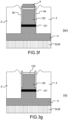
- the next step iv), illustrated by the Figure 3f consists of depositing by epitaxy an electrically semi-insulating structure 2 so as to confine the guide strip 12 in said electrically semi-insulating structure 2.
- the first dielectric layer 3a and the second dielectric layer 3b are each confined between the semi-insulating layer 2 and the guide strip 12.
- the two separating dielectric layers 3a, 3b are made of a dielectric material incompatible with the lateral deposition of the semi-insulating layer 2 by epitaxy. This makes it possible to have a controlled process for epitaxial growth of the semi-insulating structure 2, and more particularly to avoid the phenomenon of overflow of the semi-insulating structure 2 even for the case of “disoriented strip components buried in a semi-insulating SIBH”.
- the next step v), illustrated by the figure 3g consists of completely removing the dielectric etching mask 4 by selective etching with respect to the separating dielectric layers 3a, 3b.
- the dielectric layer 3 is made of silicon nitride SiN x or amorphous silicon doped with hydrogen aSi:H or an alloy of silicon and silicon nitride SRN. It is possible to selectively etch the silicon oxide SiO x with respect to the SiN x , aSi:H and SRN with a buffer solution for oxide etching comprising hydrofluoric acid HF for example.
- the next step vi), illustrated by the figure 3h consists of depositing a first electrode 14 and a second electrode 15 as described previously.
- FIG. 4 illustrates a flowchart of the first method of manufacturing the optoelectronic component according to the invention.
- the first step i) consists of providing or manufacturing an intermediate strip 12i by partially etching an initial stack of semiconductor layers deposited on a substrate.
- Step i) comprises steps ia) and ib) described previously.
- the second step ii) consists of manufacturing the first dielectric layer 3a deposited on a first lateral face 12a of the intermediate strip and the second dielectric layer 3b deposited on a second lateral face 12b of the intermediate strip 12i opposite said first lateral face 12a.
- Step ii) comprises steps iia) and iib) described previously. The remaining steps iii) to vi) have been described previously.
- FIG. 5 illustrates a microscopic sectional view (502) of a buried strip optoelectronic component D1 according to the invention in comparison with a microscopic sectional view (501) of a buried strip optoelectronic component D0 according to the state of the art.
- the phenomenon of undesirable overgrowth of the semi-insulating structure 2 on the guide strip 12 is observed in the disoriented strip component according to the state of the art.
- the microscopic sectional view (502) of a component obtained by the method according to the invention the problem of overflow of the semi-insulating structure 2 on the guide strip 12 has been resolved.
- THE figures 6a to 6h illustrate the steps of a second method P2 for manufacturing the optoelectronic component D2.
- the invention also relates to the second method P2 for manufacturing a ribbon optoelectronic component buried in a semi-insulator with two stages of burial layer growth (translation of Two-Step SIBH).
- the second method P2 makes it possible to solve the problems of overgrowth and uncontrolled epitaxial growth of the semi-insulating layer previously detailed.
- the problem of inter-diffusion of dopants between the semi-insulating layer and the ribbon is also present in Two-Step SIBH devices. More particularly, the inter-diffusion problem is accentuated during the epitaxial growth step of the semi-insulating structure at high temperature (of the order 700°C). Dopant inter-diffusion phenomena induce an increase in leakage currents in Two-Step SIBH type components in a similar manner to One-step SIBH type components.
- first method P1 and the second method P2 are linked together so as to form a single general inventive concept with a view to solving the same technical problem, namely, the use of lateral dielectric insulation layers before epitaxial recovery to solve the problem of uncontrolled growth of the semi-insulating layer which develops in an uncontrolled manner on the upper face of the guide strip as well as the problem of interdiffusion of p-dopants.
- the first step ia), illustrated by the Figure 6a is identical to step ia)' of the first method P1.
- the stack shown for the illustration of the second method P2 comprises a layer for the manufacture of diffraction grating 125' (translation of diffraction grating layer) inserted in the third layer 122'.
- step ib)' of the second process P2, illustrated by the Figure 6b is similar to step ib) of the first method P1.
- step iia)' of the second process P2, illustrated by the Figure 6c is similar to step iia) of the first method P1.
- step iib)' of the second process P2, illustrated by the Figure 6d is similar to step iib) of the first method P1.
- step iii)' of the second process P2, illustrated by the Figure 6e is similar to step iii) of the first method P1.
- the next step iv)' of the second process P2, illustrated by the Figure 6f consists of depositing by epitaxy an electrically semi-insulating structure 2 and a diffusion blocking layer 5 so as to confine at least the lower confinement structure 11 and the active zone 121 in the stack formed by the layers 2 and 5.
- the electrically semi-insulating structure 2 is a semi-insulating layer of iron-doped InP and the diffusion blocking layer 5 is a layer of ruthenium-doped or N-doped InP.
- the next step v)' of the second process P2, illustrated by the figure 6g consists of completely removing by etching the first dielectric layer 3a, the second dielectric layer 3b and the etching mask 4.
- This step can be carried out by two separate selective etching operations or by a non-selective etching operation, typically a chemical etching based on Hydrogen Fluoride HF.
- step vi)' of the second process P2, illustrated by the figure 6h consists of growing by epitaxy a cladding layer 6 made of a P-doped semiconductor.
- the cladding layer 6 encapsulates the visible part of the guide strip 12.
- Step vi)' further comprises the deposition of an electrical contact layer 123 on the upper surface of the cladding layer 6.
- the first step i)' consists of providing or manufacturing an intermediate strip 12i by partially etching an initial stack of semiconductor layers deposited on a substrate.
- Step i)' comprises steps ia)' and ib)' described previously.
- the second step ii)' consists of manufacturing the first dielectric layer 3a deposited on a first lateral face 12a of the intermediate strip and the second dielectric layer 3b deposited on a second lateral face 12b of the intermediate strip 12i opposite said first lateral face 12a.
- Step ii)' comprises steps iia)' and iib)' described previously. The remaining steps iii)' to vi)' have been described previously.
Landscapes
- Physics & Mathematics (AREA)
- Geometry (AREA)
- Condensed Matter Physics & Semiconductors (AREA)
- General Physics & Mathematics (AREA)
- Electromagnetism (AREA)
- Optics & Photonics (AREA)
- Semiconductor Lasers (AREA)
- Laminated Bodies (AREA)
Applications Claiming Priority (1)
| Application Number | Priority Date | Filing Date | Title |
|---|---|---|---|
| FR2314814A FR3157664A1 (fr) | 2023-12-21 | 2023-12-21 | Composant optoélectronique à ruban enterré dans une structure semi-isolante |
Publications (1)
| Publication Number | Publication Date |
|---|---|
| EP4576457A1 true EP4576457A1 (de) | 2025-06-25 |
Family
ID=92043153
Family Applications (1)
| Application Number | Title | Priority Date | Filing Date |
|---|---|---|---|
| EP24222328.7A Pending EP4576457A1 (de) | 2023-12-21 | 2024-12-20 | Optoelektronisches bauelement mit vergrabenem band in einer halbisolierenden struktur |
Country Status (2)
| Country | Link |
|---|---|
| EP (1) | EP4576457A1 (de) |
| FR (1) | FR3157664A1 (de) |
Citations (3)
| Publication number | Priority date | Publication date | Assignee | Title |
|---|---|---|---|---|
| JPH0728102B2 (ja) * | 1988-12-08 | 1995-03-29 | 松下電器産業株式会社 | 半導体レーザおよびその製造方法 |
| US20040013143A1 (en) * | 2000-12-15 | 2004-01-22 | Springthorpe Anthony J. | Confinement layer of buried heterostructure semiconductor laser |
| CN117254348A (zh) * | 2022-06-16 | 2023-12-19 | 美商祥茂光电科技股份有限公司 | 半导体光学装置、半导体激光器和半导体光学调制器 |
-
2023
- 2023-12-21 FR FR2314814A patent/FR3157664A1/fr active Pending
-
2024
- 2024-12-20 EP EP24222328.7A patent/EP4576457A1/de active Pending
Patent Citations (4)
| Publication number | Priority date | Publication date | Assignee | Title |
|---|---|---|---|---|
| JPH0728102B2 (ja) * | 1988-12-08 | 1995-03-29 | 松下電器産業株式会社 | 半導体レーザおよびその製造方法 |
| US20040013143A1 (en) * | 2000-12-15 | 2004-01-22 | Springthorpe Anthony J. | Confinement layer of buried heterostructure semiconductor laser |
| CN117254348A (zh) * | 2022-06-16 | 2023-12-19 | 美商祥茂光电科技股份有限公司 | 半导体光学装置、半导体激光器和半导体光学调制器 |
| US20230411931A1 (en) * | 2022-06-16 | 2023-12-21 | Applied Optoelectronics, Inc. | Semiconductor optical device with a buried heterostructure (bh) having reduced parasitic capacitance and reduced inter-diffusion |
Non-Patent Citations (1)
| Title |
|---|
| SHINODA K ET AL: "LASING OPERATION OF INGAASP-BASED INGAAS/GAAS VERTICAL-CAVITY SURFACE-EMITTING LASERS WITH A STRAIN-COMPENSATED ACTIVE REGION", JAPANESE JOURNAL OF APPLIED PHYSICS, JAPAN SOCIETY OF APPLIED PHYSICS, JP, vol. 35, PART 01, no. 9A, 1 September 1996 (1996-09-01), pages 4660 - 4663, XP000735384, ISSN: 0021-4922, DOI: 10.1143/JJAP.35.4660 * |
Also Published As
| Publication number | Publication date |
|---|---|
| FR3157664A1 (fr) | 2025-06-27 |
Similar Documents
| Publication | Publication Date | Title |
|---|---|---|
| EP3540878B1 (de) | Photonenvorrichtung, die einen laser umfasst, der optisch mit einem silizium-wellenleiter verbunden ist, und herstellungsverfahren einer solchen photonenvorrichtung | |
| EP2641304B1 (de) | Heterogener hochleistungslaser und verfahren zur herstellung des lasers | |
| EP3352312B1 (de) | Photonische vorrichtung, die einen laser umfasst, der optisch mit einem silizium-wellenleiter verbunden ist, und herstellungsverfahren einer solchen photonischen vorrichtung | |
| EP0545808B1 (de) | Optoelektronische Vorrichtung mit sehr niedrigem Serienwiderstand | |
| EP3547471B1 (de) | Laserdiode vom typ vcsel mit trägerbegrenzung, und ihr herstellungsverfahren | |
| EP3657557B1 (de) | Herstellungsverfahren einer lichtquelle, und lichtquelle | |
| EP0752743B1 (de) | Laservorrichtung mit vergrabener Struktur für integrierte photonische Schaltung und Herstellungsverfahren | |
| FR2765347A1 (fr) | Reflecteur de bragg en semi-conducteur et procede de fabrication | |
| EP4254687B1 (de) | Optoelektronische vorrichtung mit einer iii-v-halbleitermembran-laserquelle, die einen lateralen p-i-n übergang bildet | |
| FR2715770A1 (fr) | Procédé pour la réalisation d'un composant électro-optique et/ou photonique. | |
| EP0817337B1 (de) | Herstellungsverfahren für einen Oberflächenemittierenden Laser | |
| EP4009456B1 (de) | Verfahren zur herstellung eines verteilten bragg-spiegels | |
| EP0358569B1 (de) | Herstellungsverfahren für einen Halbleiterlaser mit hoher Ausgangsleistung, breiter Bandpasscharakteristik und einer vergrabenen, streifenförmigen BRS-Struktur | |
| EP4576457A1 (de) | Optoelektronisches bauelement mit vergrabenem band in einer halbisolierenden struktur | |
| EP0664588B1 (de) | Halbleiterstruktur mit virtuellem Beugungsgitter | |
| EP4481961B1 (de) | Optoelektronisches bauelement mit vergrabener spitze mit hoher leistung | |
| EP0096613B1 (de) | Halbleiter-Laservorrichtung mit einem Wellenleiter, der durch einen Gradienten im Brechungsindex gebildet ist und Verfahren zur Herstellung einer solchen Vorrichtung | |
| EP2804271B1 (de) | Elektrisch angetriebene optische parametrische Quelle auf einem Chip | |
| FR3074372A1 (fr) | Structure a gain, dispositif photonique comprenant une telle structure et procede de fabrication d'une telle structure a gain | |
| WO2025008545A1 (fr) | Puce photonique à structure hétérogène de semi-conducteur iii-v sur un deuxième semi-conducteur | |
| EP4722771A1 (de) | Siliziumintegrierte photonische iii-v-vorrichtung | |
| EP1233494A1 (de) | Halbleiterlaser miet vergrabener Streifenstruktur und Herstellungsverfahren | |
| FR2854469A1 (fr) | Procede de fabrication d'un dispositif optique semi-conducteur comportant une region munie d'une couche active a epaisseur variable | |
| WO2019122210A1 (fr) | Dispositif optoélectronique à guide d'onde semi conducteur enterré amélioré et procédé associé |
Legal Events
| Date | Code | Title | Description |
|---|---|---|---|
| PUAI | Public reference made under article 153(3) epc to a published international application that has entered the european phase |
Free format text: ORIGINAL CODE: 0009012 |
|
| STAA | Information on the status of an ep patent application or granted ep patent |
Free format text: STATUS: THE APPLICATION HAS BEEN PUBLISHED |
|
| AK | Designated contracting states |
Kind code of ref document: A1 Designated state(s): AL AT BE BG CH CY CZ DE DK EE ES FI FR GB GR HR HU IE IS IT LI LT LU LV MC ME MK MT NL NO PL PT RO RS SE SI SK SM TR |
|
| STAA | Information on the status of an ep patent application or granted ep patent |
Free format text: STATUS: REQUEST FOR EXAMINATION WAS MADE |
|
| 17P | Request for examination filed |
Effective date: 20251212 |
|
| GRAP | Despatch of communication of intention to grant a patent |
Free format text: ORIGINAL CODE: EPIDOSNIGR1 |
|
| STAA | Information on the status of an ep patent application or granted ep patent |
Free format text: STATUS: GRANT OF PATENT IS INTENDED |
|
| INTG | Intention to grant announced |
Effective date: 20260129 |