EP4576532A1 - Elektronische vorrichtung und verfahren zur ansteuerung mit unterdrückung mindestens einer energieerzeugenden phase eines elektrischen energiewandlers mit einem piezoelektrischen resonator, zugehöriges stromwandlersystem - Google Patents
Elektronische vorrichtung und verfahren zur ansteuerung mit unterdrückung mindestens einer energieerzeugenden phase eines elektrischen energiewandlers mit einem piezoelektrischen resonator, zugehöriges stromwandlersystem Download PDFInfo
- Publication number
- EP4576532A1 EP4576532A1 EP24221398.1A EP24221398A EP4576532A1 EP 4576532 A1 EP4576532 A1 EP 4576532A1 EP 24221398 A EP24221398 A EP 24221398A EP 4576532 A1 EP4576532 A1 EP 4576532A1
- Authority
- EP
- European Patent Office
- Prior art keywords
- voltage
- piezoelectric resonator
- terminals
- output
- switch
- Prior art date
- Legal status (The legal status is an assumption and is not a legal conclusion. Google has not performed a legal analysis and makes no representation as to the accuracy of the status listed.)
- Pending
Links
Images


Classifications
-
- H—ELECTRICITY
- H02—GENERATION; CONVERSION OR DISTRIBUTION OF ELECTRIC POWER
- H02M—APPARATUS FOR CONVERSION BETWEEN AC AND AC, BETWEEN AC AND DC, OR BETWEEN DC AND DC, AND FOR USE WITH MAINS OR SIMILAR POWER SUPPLY SYSTEMS; CONVERSION OF DC OR AC INPUT POWER INTO SURGE OUTPUT POWER; CONTROL OR REGULATION THEREOF
- H02M1/00—Details of apparatus for conversion
- H02M1/08—Circuits specially adapted for the generation of control voltages for semiconductor devices incorporated in static converters
- H02M1/088—Circuits specially adapted for the generation of control voltages for semiconductor devices incorporated in static converters for the simultaneous control of series or parallel connected semiconductor devices
-
- H—ELECTRICITY
- H02—GENERATION; CONVERSION OR DISTRIBUTION OF ELECTRIC POWER
- H02M—APPARATUS FOR CONVERSION BETWEEN AC AND AC, BETWEEN AC AND DC, OR BETWEEN DC AND DC, AND FOR USE WITH MAINS OR SIMILAR POWER SUPPLY SYSTEMS; CONVERSION OF DC OR AC INPUT POWER INTO SURGE OUTPUT POWER; CONTROL OR REGULATION THEREOF
- H02M1/00—Details of apparatus for conversion
- H02M1/0003—Details of control, feedback or regulation circuits
-
- H—ELECTRICITY
- H02—GENERATION; CONVERSION OR DISTRIBUTION OF ELECTRIC POWER
- H02M—APPARATUS FOR CONVERSION BETWEEN AC AND AC, BETWEEN AC AND DC, OR BETWEEN DC AND DC, AND FOR USE WITH MAINS OR SIMILAR POWER SUPPLY SYSTEMS; CONVERSION OF DC OR AC INPUT POWER INTO SURGE OUTPUT POWER; CONTROL OR REGULATION THEREOF
- H02M3/00—Conversion of DC power input into DC power output
- H02M3/01—Resonant DC/DC converters
-
- H—ELECTRICITY
- H02—GENERATION; CONVERSION OR DISTRIBUTION OF ELECTRIC POWER
- H02M—APPARATUS FOR CONVERSION BETWEEN AC AND AC, BETWEEN AC AND DC, OR BETWEEN DC AND DC, AND FOR USE WITH MAINS OR SIMILAR POWER SUPPLY SYSTEMS; CONVERSION OF DC OR AC INPUT POWER INTO SURGE OUTPUT POWER; CONTROL OR REGULATION THEREOF
- H02M1/00—Details of apparatus for conversion
- H02M1/32—Means for protecting converters other than automatic disconnection
-
- H—ELECTRICITY
- H02—GENERATION; CONVERSION OR DISTRIBUTION OF ELECTRIC POWER
- H02M—APPARATUS FOR CONVERSION BETWEEN AC AND AC, BETWEEN AC AND DC, OR BETWEEN DC AND DC, AND FOR USE WITH MAINS OR SIMILAR POWER SUPPLY SYSTEMS; CONVERSION OF DC OR AC INPUT POWER INTO SURGE OUTPUT POWER; CONTROL OR REGULATION THEREOF
- H02M3/00—Conversion of DC power input into DC power output
- H02M3/22—Conversion of DC power input into DC power output with intermediate conversion into AC
- H02M3/24—Conversion of DC power input into DC power output with intermediate conversion into AC by static converters
- H02M3/28—Conversion of DC power input into DC power output with intermediate conversion into AC by static converters using discharge tubes with control electrode or semiconductor devices with control electrode to produce the intermediate AC
- H02M3/325—Conversion of DC power input into DC power output with intermediate conversion into AC by static converters using discharge tubes with control electrode or semiconductor devices with control electrode to produce the intermediate AC using devices of a triode or a transistor type requiring continuous application of a control signal
- H02M3/335—Conversion of DC power input into DC power output with intermediate conversion into AC by static converters using discharge tubes with control electrode or semiconductor devices with control electrode to produce the intermediate AC using devices of a triode or a transistor type requiring continuous application of a control signal using semiconductor devices only
- H02M3/33569—Conversion of DC power input into DC power output with intermediate conversion into AC by static converters using discharge tubes with control electrode or semiconductor devices with control electrode to produce the intermediate AC using devices of a triode or a transistor type requiring continuous application of a control signal using semiconductor devices only having several active switching elements
- H02M3/33571—Half-bridge at primary side of an isolation transformer
-
- H—ELECTRICITY
- H02—GENERATION; CONVERSION OR DISTRIBUTION OF ELECTRIC POWER
- H02M—APPARATUS FOR CONVERSION BETWEEN AC AND AC, BETWEEN AC AND DC, OR BETWEEN DC AND DC, AND FOR USE WITH MAINS OR SIMILAR POWER SUPPLY SYSTEMS; CONVERSION OF DC OR AC INPUT POWER INTO SURGE OUTPUT POWER; CONTROL OR REGULATION THEREOF
- H02M3/00—Conversion of DC power input into DC power output
- H02M3/22—Conversion of DC power input into DC power output with intermediate conversion into AC
- H02M3/24—Conversion of DC power input into DC power output with intermediate conversion into AC by static converters
- H02M3/28—Conversion of DC power input into DC power output with intermediate conversion into AC by static converters using discharge tubes with control electrode or semiconductor devices with control electrode to produce the intermediate AC
- H02M3/325—Conversion of DC power input into DC power output with intermediate conversion into AC by static converters using discharge tubes with control electrode or semiconductor devices with control electrode to produce the intermediate AC using devices of a triode or a transistor type requiring continuous application of a control signal
- H02M3/335—Conversion of DC power input into DC power output with intermediate conversion into AC by static converters using discharge tubes with control electrode or semiconductor devices with control electrode to produce the intermediate AC using devices of a triode or a transistor type requiring continuous application of a control signal using semiconductor devices only
- H02M3/33569—Conversion of DC power input into DC power output with intermediate conversion into AC by static converters using discharge tubes with control electrode or semiconductor devices with control electrode to produce the intermediate AC using devices of a triode or a transistor type requiring continuous application of a control signal using semiconductor devices only having several active switching elements
- H02M3/33573—Full-bridge at primary side of an isolation transformer
Definitions
- the present invention relates to an electronic device for controlling an electrical energy converter capable of converting an input voltage into an output voltage.
- the invention also relates to an electrical energy conversion system comprising such a converter and such an electronic device for controlling the converter.
- the invention also relates to a method for controlling such a converter.
- a converter having two input terminals for receiving the input voltage, two output terminals for delivering the output voltage, a piezoelectric resonator having two terminals, and several switches connected to the piezoelectric resonator.
- An electronic control device comprising a measurement module configured to measure an output quantity of the converter; and a control module configured to control switching of each of the switches, to alternate phases at substantially constant voltage across the terminals of the piezoelectric resonator and phases at substantially constant charge across the terminals of said piezoelectric resonator.
- the document FR 3 125 182 A1 proposes to introduce reactive power by extending one of the voltage steps from a first half-period to a second half-period of the resonance cycle, so that this step sees a current going, then returning.
- this step sees a current going, then returning.
- This method is interesting, but requires the control of an additional angle as well as the management of energy storage.
- This method works, but requires the control of a block of several resonance cycles, i.e. several resonance periods, for example five resonance periods, because the current adjustment is no longer carried out on the scale of the period, but of said plurality of periods.
- it is also necessary to have filtering at the output over said plurality of periods, which reduces the responsiveness of the converter, and increases the size of passive filtering elements.
- the aim of the invention is then to propose an electronic control device, and an associated control method, allowing improved control of the electrical energy converter.
- the control - in the event of detection of at least one characteristic event - of the first switch in the open position for the duration of one or more successive resonance cycles of the piezoelectric resonator makes it possible to suppress the phase of the resonance cycle during which the input voltage is applied across the piezoelectric resonator, i.e. to suppress the energy supply phase to the piezoelectric resonator, also called the energizing phase.
- the detected event that is remedied is an over-energy event, when the measured output quantity is greater than a threshold quantity.
- the detected event that is remedied is a so-called minimum energy event, when the measured output quantity is greater than a target quantity and the duration during which the first switch is in the closed position during a respective resonance cycle has decreased to a minimum duration, and can then no longer decrease.
- the minimum energy event then corresponds to the case where the energizing phase is at its minimum duration, and cannot be shortened further to further reduce the energy input to the piezoelectric resonator, and at the same time the output quantity is already greater than the desired target quantity.
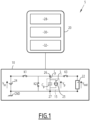
- an electronic electrical energy conversion system 5 comprises an electrical energy converter 10 comprising a piezoelectric resonator 15 and several switches K1, K2, K3 connected to the piezoelectric resonator 15; and an electronic device 20 for controlling the electrical energy converter 10.
- the electrical energy is typically a voltage, or alternatively a current or a power.
- the electronic electrical energy conversion system 5 is typically a system for converting into direct electrical energy, such as a direct-to-direct conversion system capable of converting a first direct electrical energy received at the input into a second direct electrical energy delivered at the output, or even an alternating-to-direct conversion system capable of converting alternating electrical energy received at the input into direct electrical energy delivered at the output of the conversion system 5.
- the electrical energy conversion system 5 preferably further comprises a voltage rectifier, not shown, connected to the input of the electrical energy converter 10 and capable of rectifying the AC electrical voltage received at the input of the conversion system 5 to deliver a rectified electrical voltage at the input of the converter 10, the electrical energy converter 10 preferably being a DC-DC converter capable of converting DC electrical energy into another DC electrical energy.
- the voltage rectifier is for example a rectifier bridge, such as a diode bridge.
- the voltage rectifier is formed in whole or in part by switches of the converter 10, for example via bidirectional voltage switches.
- the electrical energy converter 10 is preferably a DC-DC converter, and is also called a DC-DC converter.
- the DC-DC converter generally has the role of regulating a supply voltage V out of a load 22 to a stable value, being powered by an energy source 24 providing a substantially continuous voltage Vin.
- the energy source 24 is for example a battery or a solar panel.
- the electrical energy converter 10 is then configured to raise the value of the DC voltage between its input and its output, and is then also called a step-up DC-DC converter, or a high-step-up DC-DC converter; or is configured to lower the value of the DC voltage between its input and its output, and is then called a step-down DC-DC converter, with also a variant of a high-step-down DC-DC converter.
- the value of the input voltage typically corresponds to the voltage V in of the energy source 24, and the value of the output voltage corresponds to the voltage V out at the terminals of the load 22, the voltage Vin then being greater than the voltage V out .
- the value of the input voltage also typically corresponds to the voltage Vin of the energy source 24, and the value of the output voltage corresponds to the voltage V out at the terminals of the load 22, the voltage V in then being lower than the voltage V out .
- the value of the input voltage corresponds for example to the voltage difference (V in -V out ), and the value of the output voltage corresponds for example to the voltage V out , the voltage difference (V in -V out ) being significantly greater than the voltage V out .
- the value of the input voltage corresponds for example to the voltage difference (V in -V out ), and the value of the output voltage corresponds to the voltage V out at the terminals of the load 22, the voltage difference (V in -V out ) being greater than the voltage V out .
- the electrical energy converter 10 comprises the piezoelectric resonator 15, and the control device 20 is configured to operate the piezoelectric material of the piezoelectric resonator 15 at its resonance in order to exploit charge transfer phases making it possible to dispense with the use of an inductive element, while regulating the output voltage by maintaining the resonance of the piezoelectric material, that is to say with repeated switching cycles at an operating frequency dependent on the resonance frequency of the piezoelectric resonator 15, and by adjusting the durations of the respective switching phases within the resonance cycle.
- the mechanical oscillation of the piezoelectric resonator 15 is approximately sinusoidal. An increase or decrease in the stored energy over a period leads respectively to an increase or a decrease in the oscillation amplitude. Furthermore, during a phase with substantially constant charge at the terminals of the piezoelectric resonator 15, that is to say when the piezoelectric resonator 15 is placed in a substantially open electrical circuit, with a low exchange of electrical charges between the piezoelectric resonator 15 and the outside, an increase in the amplitude of the oscillations causes an increase in the speed of variation of the voltage V p at the terminals of the piezoelectric resonator 15, and during a phase with substantially constant voltage at the terminals of the piezoelectric resonator 15, this increase in oscillation amplitude leads to an increase in the current exchanged between the piezoelectric resonator 15 and the outside.
- substantially constant charge is meant an exchange of a charge with the outside which is less than 30% of the charge which would have been exchanged with the outside if the voltage had been kept constant.
- substantially constant charge is meant a variation in charge less than 30% of the charge which would have been exchanged with the outside of the piezoelectric resonator 15 if the voltage across the terminals of the piezoelectric resonator 15 had been kept constant over the time period considered.
- substantially open electrical circuit means a circuit in which a possible leakage current leads to a variation in charge of the piezoelectric resonator 15 of less than 30% of the charge which would have been exchanged with the exterior of the piezoelectric resonator 15 if the voltage across the terminals of the piezoelectric resonator 15 had been kept constant over the time period considered.
- substantially constant voltage is meant a voltage variation of less than 20%, preferably less than 10%, of the input or output voltage of the converter 10. For example, if the input voltage of the converter 10 is equal to 100V, then the voltage variation during each phase at substantially constant voltage, i.e. on each step at substantially constant voltage, is less than 20% of this voltage, i.e. less than 20V; preferably less than 10% of this voltage, i.e. less than 10V.
- the converter 10 then comprises several switches K1, K2, K3 capable of being controlled to alternate phases at substantially constant voltage and phases at substantially constant load at the terminals of the piezoelectric resonator 15.
- This alternation of phases at substantially constant voltage and phases at substantially constant load is typically carried out within periods of substantially constant duration corresponding to the operating frequency of the converter 10, depending on the oscillation frequency, also called natural frequency, of the piezoelectric resonator 15.
- the phases with substantially constant load allow, in steady state or permanent, to pass from one constant voltage to another and to close the switches which must be closed when the voltage at their terminals is preferably zero in order to have a so-called zero voltage switching, also called ZVS switching (from the English Zero Voltage Switching ) .
- Each switch of the converter 10, namely a first switch K1, a second switch K2, and in addition a third switch K3, comprises for example a transistor and an antiparallel diode (not shown) intrinsic to the transistor.
- the transistor is, for example, an insulated gate field effect transistor, also called a MOSFET (from the English Metal Oxide Semiconductor Field Effect Transistor ) .
- the transistor 50 is a bipolar transistor; an insulated gate bipolar transistor, also called an IGBT (from the English Insulated Gate Bipolar Transistor ); a silicon (Si)-based transistor, a GaN (from the English Gallium Nitride )-based transistor ; a silicon carbide (SiC)-based transistor, or a diamond-based transistor, or a thyristor, or a mechanical switch, such as a MEMS (from the English MicroElectroMechanical System) microswitch.
- a MEMS from the English MicroElectroMechanical System
- the first switch K1 is connected between one of the input terminals and the resonator 15, the first switch K1 being switchable between an open position and a closed position in which the input voltage Vin is applied across the resonator 15.
- the second switch K2 is connected across the terminals of the piezoelectric resonator 15, the second switch K2 being switchable between an open position and a closed position in which the voltage is zero across the terminals of the resonator 15.
- the third switch K3 is connected between one of the output terminals and the resonator 15, the third switch K3 being switchable between an open position and a closed position in which energy from the resonator 15 is returned to the output voltage V out .
- the oscillation frequency is the frequency at which the resonator 12, such as the piezoelectric resonator 15, oscillates and consequently its current I L on its motional branch (RLC branch) of its equivalent model around the selected resonance mode.
- the current I L can be deduced either by observing the evolution of the voltage V p when the resonator is isolated or by observing its output current I p during the constant voltage phases.
- the conversion cycle is synchronized to a mechanical movement of the piezoelectric resonator 15, and the driving frequency is then set to the mechanical oscillation frequency. In practice, this oscillation frequency depends on the operating point of the converter 10: values of the three voltage steps and of the output current.
- the operating frequency of the converter 10 is then between these two resonance and antiresonance frequencies of the piezoelectric resonator 15.
- the operating point varies slowly with respect to the oscillation frequency of the piezoelectric resonator 15.
- the operating point typically varies at less than 10kHz, while the oscillation frequency of the piezoelectric resonator 15 is typically greater than or equal to 100kHz. As a result, the operating frequency of the converter 10 changes little from one period to the next.
- the total number of substantially constant voltage phases and substantially constant load phases across the piezoelectric resonator 15 during a resonance cycle is generally greater than or equal to six in a nominal operating mode of the converter 10. In the example of the Figure 1 , this total number of phases is equal to six in nominal operating mode of the converter 10.
- the piezoelectric resonator 15 is known per se, and is typically modeled, close to the resonance mode used, in the form of a capacitor Cp and the resonant branch 25 connected in parallel with the capacitor Cp, the capacitor Cp and the resonant branch 25 being connected between first 26 and second 27 electrodes of the piezoelectric resonator 15.
- the first 26 and second 27 electrodes form the terminals of the piezoelectric resonator 15.
- the piezoelectric resonator 15 comprises a single piezoelectric element.
- the piezoelectric resonator 15 comprises several piezoelectric elements connected in series. Alternatively, the piezoelectric resonator 15 comprises several piezoelectric elements connected in parallel. Alternatively, the piezoelectric resonator 15 comprises a piezoelectric element and an auxiliary capacitor connected in series. Alternatively, the piezoelectric resonator 15 comprises a piezoelectric element and an auxiliary capacitor connected in parallel. As a further variant, the piezoelectric resonator 15 comprises an arrangement of several parallel branches, each branch comprising one or more piezoelectric elements connected in series or an auxiliary capacitor.
- the auxiliary capacitor is advantageously of greater capacity, more preferably at least three times greater, than a reference capacity of the piezoelectric element(s), such as the capacity of the capacitor Cp in the example of the Figure 1 , each piezoelectric element being modeled as a capacitor and a resonant branch connected in parallel to the capacitor, the reference capacitance being the capacitance of said capacitor.
- the first switch K1 is connected between a positive input terminal and the first electrode 26 of the resonator 15
- the second switch K2 is connected between the first 26 and second 27 electrodes of the piezoelectric resonator 15
- the third switch K3 is connected between the first electrode 26 of the resonator 15 and a positive output terminal and the resonator 15.
- positive terminal the person skilled in the art will understand that this is the terminal which is at the highest potential of the input voltage V in , respectively of the output voltage V out .
- the negative input and output terminals are connected to an electrical ground GND.
- the resonant branch 25 is typically an RLC branch formed of an auxiliary capacitor, a resistor and an inductor connected in series (not shown).
- the voltage V p across the terminals of the piezoelectric resonator 15 then typically corresponds to the voltage across the capacitor Cp.
- the capacity of the auxiliary capacitor is advantageously greater than the capacity of the capacitor Cp, in particular at least three times greater.
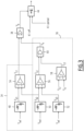
- the control device 20 comprises a measurement module 28, a detection module 30 and a control module 32.
- the measurement module 28, the detection module 30, and the control module 32 are for example each produced in the form of an electronic circuit comprising one or more electronic components, and in particular comparators when comparisons are carried out.
- the measurement module 28, the detection module 30, and the control module 32 are each produced in the form of a programmable logic component, such as an FPGA (Field Programmable Gate Array), or in the form of an integrated circuit, such as an ASIC (Application Specific Integrated Circuit) or even in the form of a computer, such as a microcontroller, a processor.
- the measurement module 28, the detection module 30 and the control module 32 are implemented together within a single hardware component, such as a single programmable logic component, a single integrated circuit, or a single computer.
- the measuring module 28 is configured to measure an output quantity G out .
- the output quantity G out is, for example, the output voltage V out .
- the output quantity G out is an output current I out .
- the output quantity G out is an output power P out .
- the detection module 30 is configured to detect at least one characteristic event dependent on the measured output quantity G out .
- the detection module 30 is advantageously capable of detecting an over-energy event and/or a minimum energy event.
- a respective characteristic event is advantageously the over-energy event, or the minimum energy event.
- the over-energy event is detected when the output quantity G out , such as the output voltage V out , is greater than a threshold quantity G thr .
- the minimum energy event is detected when the output quantity Gout, such as the output voltage V out , is greater than a target quantity G tar and a duration D K1 during which the first switch K1 is in the closed position during a respective resonance cycle has decreased to a minimum duration D min .
- the threshold quantity G thr is typically greater than the target quantity G tar .
- the target quantity G tar then forms a second threshold quantity, distinct from the threshold quantity G tbr , and preferably less than the threshold quantity G thr .
- the threshold quantity G thr is equal to a multiple of the target quantity G tar .
- the multiple is typically between 1.02 and 1.3; preferably between 1.02 and 1.1; more preferably equal to 1.05.
- the converter 10 has a low power limit, characteristic of the elements making up the energy converter 10.
- the minimum duration D min then depends on the low power limit.
- the minimum duration D min cannot in fact tend towards zero.
- the minimum duration D min is for example of the order of 2 nanoseconds.
- the control module 32 is configured to control a switching of each of the switches K1, K2 and K3, typically to alternate phases at substantially constant voltage across the terminals of the piezoelectric resonator 15 and phases at substantially constant charge across the terminals of said piezoelectric resonator 15.
- the control module 32 is, according to the invention, configured to, in the event of detection of at least one characteristic event, control the first switch K1 in the open position for the duration of at least one resonance cycle of the piezoelectric resonator 15.
- the first switch K1 is advantageously controlled to remain in the open position as long as at least one characteristic event is detected by the detection module 30.
- the first switch K1 is advantageously commanded, then held in the open position as long as the presence of at least one characteristic event is detected.
- the measurement module 28 comprises an adder 33 connected to the output of a unit, not shown, for measuring the output quantity G out .
- the detection module 30 comprises a first unit 34 for detecting the over-energy event, a second unit 36 for detecting the minimum energy event and an OR logic gate 38 (from the English OR logic gate ) .
- the control module 32 comprises a corrector 40, a generator 42 of a control signal, a multiplexer 44 a unit 46 for controlling a switch, such as the first switch K1.
- the adder 33 is capable of receiving on the one hand the output quantity G out , such as the output voltage V out , and on the other hand a reference quantity G ref , such as a reference voltage V ref , then of delivering at output an error ⁇ corresponding to the difference between the output quantity G out and the reference quantity G ref .
- the adder 33 is typically configured to subtract the reference quantity G ref from the output quantity G out .
- the first unit 34 for detecting the over-energy event is capable of receiving as input the output quantity G out , such as the output voltage V out , and of delivering as output a voltage V c1 , the voltage V c1 typically being in the form of a square-wave voltage with a high or low logic level depending on whether the over-energy event has been detected or not.
- the second unit 36 for detecting the minimum energy event is connected to the output of the corrector 40.
- the second detection unit 36 is also capable of receiving as input the output quantity G out , such as the output voltage V out , and of delivering as output a voltage V a , the voltage V a typically also being in the form of a square wave voltage with a high or low logic level depending on whether the minimum energy event has been detected or not.
- the OR logic gate 38 is connected to the output of the first unit 34 and the second unit 36, and then able to receive the voltage V c1 and the voltage V a as input.
- the OR logic gate 38 is capable of delivering a voltage V b as output, the voltage V b typically also being in the form of a square wave voltage with a high logic level if V c1 and/or V a have(s) a high logic level, and with a low logic level otherwise.
- the corrector 40 is typically configured to perform a regulation of the output quantity G out with respect to the reference quantity G ref , by receiving as input the error ⁇ from the adder 33, corresponding to the output quantity G out minus the reference quantity G ref , and then performing an integration of this error ⁇ .
- the corrector 40 comprises for example an operational amplifier 40A, an electrical resistor 40B and a feedback loop with a capacitor 40C.
- the feedback loop connects the output of the operational amplifier 40A to its negative input.
- the electrical resistance 40B is connected between the input of the corrector 40 receiving the error ⁇ and the negative input of the operational amplifier 40A. It is understood that other types of correctors 40 can be used.
- the control signal generator 42 is connected to the output of the corrector 40, and is configured to generate a periodic control signal for the first switch K1 denoted K1-period as a function of the signal at the output of the corrector 40.
- the multiplexer 44 is connected to the output of the generator 42 and the OR logic gate 38, and is then able to receive as input the control signals for opening K1-off and periodic closing K1-period, as well as the voltage V b .
- the multiplexer 44 is for example capable of selecting the opening control signal K1-off if the voltage V b has a high logic level, and of not selecting a control signal in particular if the voltage V b has a low logic level.
- the control unit 46 is connected to the output of the multiplexer 44, and then able to receive as input the control signal for opening K1-off or respectively for periodic closing K1-period, coming from the multiplexer 44.
- the control unit 46 is connected to the input of the first switch K1 and is configured to apply the control signal, either for opening and keeping open K1-off, or for periodic closing K1-period, to a control electrode of the first switch K1, such as a gate electrode when the first switch K1 comprises a transistor such as a MOSFET or an IGBT.
- the first unit 34 for detecting the over-energy event comprises a first voltage divider 48 and a first comparator 54.
- the second minimum energy event detection unit 36 comprises a second voltage divider 50, a third voltage divider 52, a second comparator 56, a third comparator 58 and an AND logic gate 60 .
- the voltage dividers 48, 50, 52 are typically configured to deliver an output voltage lower than their input voltage.
- the first voltage divider 48 is capable of receiving as input the reference quantity G ref , such as the reference voltage V ref , and capable of delivering as output a voltage V d1 , the voltage V d1 being a fraction of the input voltage V ref .
- the second voltage divider 50 is capable of receiving as input the output quantity G out , such as the output voltage V out , and capable of delivering as output a voltage V d2 , the voltage V d2 being a fraction of the input voltage V out .
- the third voltage divider 52 is capable of receiving as input the reference quantity G ref , such as the reference voltage V ref , and capable of delivering as output a voltage V d3 , the voltage V d3 being a fraction of the input voltage V ref .
- the division factors implemented respectively by the first, second and third voltage dividers 48, 50, 52 are such that, on the one hand, the ratio between the voltages V d2 and V d3 is equal to the ratio between the output quantity G out and the target quantity G tar , in particular equal to the ratio between the output voltage V out and a target voltage V tar ; and on the other hand, that the ratio between the voltages V d2 and V d1 is equal to the ratio between the output quantity G out and the threshold quantity G thr , in particular equal to the ratio between the output voltage V out and a threshold voltage V thr .
- the first comparator 54 is connected to the output of the first voltage divider 48 and the second voltage divider 50, and then capable of receiving the voltage V d1 and the voltage V d3 as input.
- the first comparator 54 is capable of delivering the voltage V c1 as output, the voltage V c1 typically being in the form of a square wave voltage with a high logic level if the voltage V d2 is greater than the voltage V d1 , and with a low logic level otherwise.
- the second comparator 56 is connected to the output of the second voltage divider 50 and the third voltage divider 52, and then capable of receiving the voltage V d2 and the voltage V d3 as input.
- the second comparator 56 is capable of delivering as output a voltage V c2 , the voltage V c2 typically being in the form of a square wave voltage with a high logic level if the voltage V d2 is greater than the voltage V d3 , and with a low logic level otherwise.
- the third comparator 58 is capable of receiving as input a voltage V CI and a voltage V t1 .
- the voltage V CI is a voltage linked to the minimum duration D min and the voltage V t1 is a voltage linked to the duration D K1 of closing of the switch K1 during the respective cycle, the voltages V CI and V t1 being chosen so that the ratio between the voltages V t1 and V Cl is equal to the ratio between the durations D K1 and D min .
- the third comparator 58 is capable of delivering the voltage V c3 as output, the voltage V c3 typically being in the form of a square wave voltage with a high logic level if the voltage V t1 becomes lower than the voltage V CI , and with a low logic level otherwise.
- the AND logic gate 60 is connected to the output of the second comparator 56 and the third comparator 58, and is then able to receive the voltage V c2 and the voltage V c3 as input.
- the AND logic gate 60 is capable of delivering a voltage V a as output, the voltage V a typically also being in the form of a square wave voltage with a high logic level if the voltages V c2 and V c3 have a high logic level, and with a low logic level otherwise.
- a first switching time instant corresponds to the closing of the first switch K 1 for the first mode M1, respectively of the third switch K 3 for the second mode M2, and the voltage V p across the terminals of the piezoelectric resonator 15 is then substantially constant and equal to the input voltage V in according to the first mode M1, or to the output voltage V out according to the second mode M2.
- t 1 begins a first phase I lasting until the opening of the switch which was closed at the first switching time instant t 1 .
- a second switching time instant corresponds to the opening of the first switch K 1 for the first mode M1, respectively of the third switch K 3 for the second mode M2, and the voltage V p at the terminals of the piezoelectric resonator 15 then changes from a previous voltage V in according to the first mode M1, or V out according to the second mode M2, to an open circuit position.
- t 2 begins a second phase II lasting until a time instant t 3 corresponding to a zero crossing of the current I L flowing in the piezoelectric resonator 15.
- the time instant t 2 was defined so that at the instant time t 3 , the voltage V p at the terminals of the piezoelectric resonator 15 reaches a value corresponding to the value allowing zero voltage switching of the corresponding switch.
- a third phase III begins, at a voltage substantially constant at zero value according to the first mode M1 via the closing of the second switch K2, or the input voltage V in according to the second mode M2 via the closing of the first switch K 1 , and lasts until a time instant t 4 which forms an adjustment parameter of the converter 10, this time instant t 4 making it possible to define the voltage, the current or even the desired power at the output of the converter 10.
- the time instant t 4 then corresponds to the end of the third phase III and to the instant at which the second switch K 2 according to the first mode M1, or respectively the first switch K 1 according to the second mode M2, must then be open, the time instant t 4 forming a fourth switching time instant corresponding to the opening of the second switch K 2 according to the first mode M1, or respectively of the first switch K 1 according to the second mode M2.
- a fourth phase IV begins, corresponding to a phase with substantially constant load, or else in substantially open circuit, this fourth phase IV lasting until a time instant t 5 defined by the transition to a new predefined value of the voltage V p at the terminals of the piezoelectric resonator 15.
- the time instant t 5 forming the end of the fourth phase IV typically corresponds to the closing of the third switch K 3 according to the first mode M1, or respectively of the second switch K 2 according to the second mode M2, the time instant t 5 then forming a fifth switching time instant.
- t 5 begins a fifth phase V corresponding to a phase at substantially constant voltage at the output voltage V out according to the first mode M1 via the closing of the third switch K3, or at the zero value according to the second mode M2 via the closing of the second switch K2.
- This fifth phase V lasts until a time instant t 0 , or again until a time instant t 6 modulo the period T of the resonance cycle defined by the zero crossing of the current I L flowing in the piezoelectric resonator 15, and according to a monotony opposite to that of the zero crossing at the time instant t 3 .
- the time instant t 6 is equal to the sum of the time instant t 0 and the period T of the resonance cycle, and is also noted (t 0 +T).
- the time instant t 6 corresponds to the end of a resonance cycle of the piezoelectric resonator 15, the cycle represented having been defined in relation to the time instants of zero crossing of the current I L flowing in the piezoelectric resonator 15, and not in relation to the first switching time instant t 1 .
- the time instant t 0 is obtained via the opening of the third switch K 3 according to the first mode M1, or respectively of the second switch K2 according to the second mode M2, and then forms a sixth switching time instant.
- this sixth phase VI corresponding to a phase with substantially constant charge
- this sixth phase VI phase flowing between the time instant t 6 and the time instant t 6 +t 1 , or between the time instant t 0 and the time instant t 1 in the example of the Figure 5 , it being understood that the time instant t 6 corresponds to the time instant t 0 to within one resonance cycle.
- the end of this sixth phase VI corresponds to the moment when the voltage V p at the terminals of the piezoelectric resonator 15 reaches the input voltage V in according to the first mode M1, or the output voltage V out according to the second mode M2.
- phase during which the electrical energy is transferred to the piezoelectric resonator 15, also called the energizing phase of the cycle is the phase corresponding to the closing of the first switch K1, that is to say the first phase I according to the first operating mode M1, and respectively the third phase III according to the second operating mode M2.
- This energizing phase ends with the opening of the first switch K1 at the time instant t 2 according to the first mode M1, and respectively at the time instant t 4 according to the second mode M2.
- This time instant of opening of the first switch K1 is defined as the time instant allowing the piezoelectric resonator 15 to receive a quantity of energy equal to the quantity of energy taken by the output load 22 during the period T.
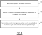
- the measuring module 28 of the control device 20 measures the output quantity G out , such as the output voltage V out , of the converter 10 at the terminals of the load 22.
- the detection module 30 then detects at least one characteristic event dependent on the measured output quantity G out .
- the at least one characteristic event can be the over-energy event and/or the minimum energy event.
- the detection module 30 receives the output quantity G out measured by the measurement module 28.
- the over-energy event is detected within the first unit 34. For example, when the output quantity G out is the output voltage V out , at the output of the first voltage divider 48 and the second voltage divider 50, the voltages V d1 and V d2 are compared within the first comparator 54. If the voltage V d2 from the second divider bridge 50 receiving the output voltage V out is greater than the voltage V d1 , representative of the threshold voltage V thr , the over-energy event is detected by the first comparator 54, and the voltage V c1 at the output of the first comparator 54 then has a high logic level.
- the over-energy event is therefore detected if the output quantity G out is greater than the threshold quantity G thr .
- the detection module 30 receives the output quantity G out measured by the measurement module 28.
- the minimum energy event is detected within the second unit 36. For example, when the output quantity G out is the output voltage V out , at the output of the second voltage divider 50 and the third voltage divider 52, the voltages V d2 and V d3 are compared within the second comparator 56. If the voltage V d2 from the second divider bridge 50 receiving the output voltage V out is greater than the voltage V d3 , representative of the target voltage V tar , then the voltage V c2 at the output of the second comparator 56 has a high logic level. Furthermore, the voltages V CI and V t1 are also compared within the third comparator 58.
- the voltage V t1 linked to the duration D K1 of closing of the switch K1 becomes less than or equal to the voltage V CI linked to the minimum duration D min , then the voltage V c3 at the output of the third comparator 58 also has a high logic level.
- the AND logic gate 60 therefore also has a high logic level at its output, which corresponds to the detection of the minimum energy event.
- the minimum energy event is then detected if the output quantity G out is greater than the target quantity G tar and if the duration D K1 of closing of the switch K1 is less than or equal to the minimum duration D min .
- the presence of a high level on one of the voltages V c1 or V a causes the presence of a high level on the voltage V b which corresponds to the detection of at least one characteristic event.
- This detection in the form of the voltage V b at the high level, is then transmitted to the control module 32, and in particular to the multiplexer 44.
- the multiplexer 44 selects the opening control signal K1-off.
- the first switch K1 will then be forced into the open position, i.e. maintained in the open position.
- the electrical converter 10 is therefore no longer in its nominal operating mode, and passes into a particular operating mode during which the number of phases is reduced by one unit, in particular with one less phase at substantially constant voltage, and is typically equal to 5 for the electrical converter 10 of the example of the Figure 1 .
- the suppressed phase is the energizing phase of the electric resonator 15, typically the first phase I according to the first operating mode M1, and respectively the third phase III according to the second operating mode M2.
- control module 32 suppresses the energizing phase by controlling the opening of the first switch K1 as long as the detection module 30 detects the presence of the at least one characteristic event, the suppression of the energizing phase therefore being able to be consecutive over several cycles, as shown in Figure 6 .
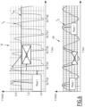
- FIG. 6 represents the curve of the voltage V p at the terminals of the piezoelectric resonator 15, on the one hand for a first example noted SE of detection of the over-energy event, and on the other hand for a second example EM of detection of the minimum energy event.
- the energizing phase such as the first phase I, also noted phase 1
- the energizing phase is suppressed during several successive resonance cycles of the piezoelectric resonator 15, and during at least five successive cycles in this first example SE, this until the output quantity G out again becomes lower than the threshold quantity G thr .
- the energizing phase such as the first phase I, also noted phase 1
- the converter 10 is also suppressed during several successive resonance cycles of the piezoelectric resonator 15, in this case during two successive cycles, and the converter 10 then returns to nominal operating mode.
- the converter returns to nominal operating mode as soon as the energy event minimum is no longer detected, i.e. as soon as the output quantity G out becomes lower than the target quantity G tar again.
- control module 32 in the event of detection of at least one characteristic event, is configured to control the first switch K1 in the open position for the duration of at least one resonance cycle of the piezoelectric resonator 15, while not modifying during said duration the control of the other switches K2, K3 connected to the piezoelectric resonator 15.
- the invention corresponds to the superposition of an exceptional state, namely the control of the first switch K1 in the open position for said duration in the event of detection of at least one characteristic event, to a normal regulated operating state.
Landscapes
- Engineering & Computer Science (AREA)
- Power Engineering (AREA)
- Dc-Dc Converters (AREA)
Applications Claiming Priority (1)
| Application Number | Priority Date | Filing Date | Title |
|---|---|---|---|
| FR2314512A FR3157031A1 (fr) | 2023-12-19 | 2023-12-19 | Dispositif électronique et procédé de pilotage, avec suppression d’au moins une phase énergisante, d’un convertisseur d’énergie électrique comportant5 un résonateur piézoélectrique, système de conversion d’énergie électrique associé |
Publications (1)
| Publication Number | Publication Date |
|---|---|
| EP4576532A1 true EP4576532A1 (de) | 2025-06-25 |
Family
ID=90720991
Family Applications (1)
| Application Number | Title | Priority Date | Filing Date |
|---|---|---|---|
| EP24221398.1A Pending EP4576532A1 (de) | 2023-12-19 | 2024-12-19 | Elektronische vorrichtung und verfahren zur ansteuerung mit unterdrückung mindestens einer energieerzeugenden phase eines elektrischen energiewandlers mit einem piezoelektrischen resonator, zugehöriges stromwandlersystem |
Country Status (3)
| Country | Link |
|---|---|
| US (1) | US20250233508A1 (de) |
| EP (1) | EP4576532A1 (de) |
| FR (1) | FR3157031A1 (de) |
Citations (6)
| Publication number | Priority date | Publication date | Assignee | Title |
|---|---|---|---|---|
| US6317342B1 (en) * | 1999-08-24 | 2001-11-13 | Munetix, Inc. | Electrostatic microresonant power conversion |
| FR3086471A1 (fr) | 2018-09-21 | 2020-03-27 | Commissariat A L'energie Atomique Et Aux Energies Alternatives | Convertisseur de puissance |
| FR3086472A1 (fr) | 2018-09-21 | 2020-03-27 | Commissariat A L'energie Atomique Et Aux Energies Alternatives | Convertisseur de puissance |
| US20210399638A1 (en) * | 2020-06-18 | 2021-12-23 | Texas Instruments Incorporated | Closed Loop Control for Piezoelectric-Based Power Converters |
| EP4080747A1 (de) * | 2021-04-21 | 2022-10-26 | Commissariat à l'énergie atomique et aux énergies alternatives | Elektronische vorrichtung und verfahren zur steuerung eines elektrischen energiewandlers mit einem piezoelektrischen element und entsprechendes elektronisches system zur umwandlung von elektrischer energie |
| EP4117161A1 (de) * | 2021-07-07 | 2023-01-11 | Commissariat à l'énergie atomique et aux énergies alternatives | Elektronische vorrichtung und verfahren zur steuerung mit zusätzlichem freiheitsgrad eines elektrischen energiewandlers, der ein piezoelektrisches element enthält, und entsprechendes elektronisches system zur umwandlung von elektrischer energie |
-
2023
- 2023-12-19 FR FR2314512A patent/FR3157031A1/fr active Pending
-
2024
- 2024-12-18 US US18/986,280 patent/US20250233508A1/en active Pending
- 2024-12-19 EP EP24221398.1A patent/EP4576532A1/de active Pending
Patent Citations (7)
| Publication number | Priority date | Publication date | Assignee | Title |
|---|---|---|---|---|
| US6317342B1 (en) * | 1999-08-24 | 2001-11-13 | Munetix, Inc. | Electrostatic microresonant power conversion |
| FR3086471A1 (fr) | 2018-09-21 | 2020-03-27 | Commissariat A L'energie Atomique Et Aux Energies Alternatives | Convertisseur de puissance |
| FR3086472A1 (fr) | 2018-09-21 | 2020-03-27 | Commissariat A L'energie Atomique Et Aux Energies Alternatives | Convertisseur de puissance |
| US20210399638A1 (en) * | 2020-06-18 | 2021-12-23 | Texas Instruments Incorporated | Closed Loop Control for Piezoelectric-Based Power Converters |
| EP4080747A1 (de) * | 2021-04-21 | 2022-10-26 | Commissariat à l'énergie atomique et aux énergies alternatives | Elektronische vorrichtung und verfahren zur steuerung eines elektrischen energiewandlers mit einem piezoelektrischen element und entsprechendes elektronisches system zur umwandlung von elektrischer energie |
| EP4117161A1 (de) * | 2021-07-07 | 2023-01-11 | Commissariat à l'énergie atomique et aux énergies alternatives | Elektronische vorrichtung und verfahren zur steuerung mit zusätzlichem freiheitsgrad eines elektrischen energiewandlers, der ein piezoelektrisches element enthält, und entsprechendes elektronisches system zur umwandlung von elektrischer energie |
| FR3125182A1 (fr) | 2021-07-07 | 2023-01-13 | Commissariat à l'énergie atomique et aux énergies alternatives | Dispositif électronique et procédé de pilotage avec degré de liberté supplémentaire d’un convertisseur d’énergie électrique comportant un élément piézoélectrique, système électronique de conversion d’énergie électrique associé |
Non-Patent Citations (4)
| Title |
|---|
| B. POLLETG. DESPESSEF. COSTA: "A New Non-Isolated Low-Power Inductorless Piezoelectric DC-DC Converter", IEEE TRANSACTIONS ON POWER ELECTRONICS, vol. 34, no. 11, XP011744096, DOI: 10.1109/TPEL.2019.2900526 |
| E. A. STOLTW. D. BRAUNJ. M. RIVAS-DAVILA: "Workshop on Control and Modeling for Power Electronics (COMPEL", 2022, IEEE, article "Fundamental examination of multiple potential passive component technologies for future power electronics" |
| J. J. PIELJ. D. BOLESJ. H. LANGD. J. PERREAULT: "Workshop on Control and Modelling of Power Electronics (COMPEL", 2021, IEEE, article "Feedback Control for a Piezoelectric-Resonator-Based DC-DC Power Converter" |
| M. TOUHAMIG. DESPESSEF. COSTAB. POLLET: "European Conference on Power Electronics and Applications (EPE'20 ECCE Europe", 2020, article "Implementation of Control Strategy for Step-down DC-DC Converter Based on Piezoelectric Resonator" |
Also Published As
| Publication number | Publication date |
|---|---|
| US20250233508A1 (en) | 2025-07-17 |
| FR3157031A1 (fr) | 2025-06-20 |
Similar Documents
| Publication | Publication Date | Title |
|---|---|---|
| EP3627688B1 (de) | Leistungswandler | |
| EP3627687A1 (de) | Leistungswandler | |
| EP0654887B1 (de) | Unterbrechungsfreie Stromversorgung mit gemeinsamem Nullleiter und Doppelaufwärtskonverter | |
| EP4191854B1 (de) | Elektronische vorrichtung und verfahren zur gleichtaktfreien steuerung eines elektrischen energiewandlers mit zwei piezoelektrischen elementen, elektronisches stromwandlersystem dafür | |
| FR2885237A1 (fr) | Dispositif de commande d'un convertisseur de tension continue a commutation et son utilisation pour maximiser la puissance delivree par un generateur photovoltaique | |
| EP2594007B1 (de) | Vorrichtung zum spannungsausgleich an den klemmen eines kondensators in einer kondensatoranordnung sowie spannungsumwandlungssystem mit einer solchen ausgleichsvorrichtung | |
| FR2924873A1 (fr) | Circuit de controle du courant dans un organge electrique de commande ou de la tension aux bornes dudit organe electriqu electrique de commande | |
| EP3807985B1 (de) | Wechselstrom-gleichstrom-wandler | |
| EP4576532A1 (de) | Elektronische vorrichtung und verfahren zur ansteuerung mit unterdrückung mindestens einer energieerzeugenden phase eines elektrischen energiewandlers mit einem piezoelektrischen resonator, zugehöriges stromwandlersystem | |
| EP4117161B1 (de) | Steuerung und steuerungsverfahren mit zusätzlichem freiheitsgrad für einen piezoelektrischen energiewandler | |
| EP1564876B1 (de) | Schweisseinrichtung mit sanfschaltendem Quasi-resonanzwechselrichter | |
| EP4080747A1 (de) | Elektronische vorrichtung und verfahren zur steuerung eines elektrischen energiewandlers mit einem piezoelektrischen element und entsprechendes elektronisches system zur umwandlung von elektrischer energie | |
| EP4576531A1 (de) | Elektronische vorrichtung und verfahren zur steuerung eines elektrischen energiewandlers mit synchronisiertem dreiecksignal und stromwandlersystem dafür | |
| EP3843255A1 (de) | Schaltung zur steuerung der eingangsimpedanz einer rekuperator-schnittstelle | |
| EP4576530A1 (de) | Elektronische vorrichtung und verfahren zur steuerung eines elektrischen energiewandlers mit resonator, zugehöriges stromwandlersystem | |
| EP2940849A2 (de) | Elektrische stromversorgung und steuerverfahren einer solchen elektrischen stromversorgung | |
| EP4191852B1 (de) | Stromwandler mit piezoelektrischem element und schalthilfsschaltung(en), elektronisches stromwandlersystem | |
| EP4191853B1 (de) | Elektrischer energiewandler mit mindestens einem paar piezoelektrischer anordnungen und mindestens einem komplementären direktverbindungsschalter, umwandlungssystem und steuerungsverfahren dafür | |
| FR2846485A1 (fr) | Dispositif de commande electronique d'un actionneur piezoelectrique ultrasonore | |
| WO2020016140A1 (fr) | Procede de gestion des commutations d'un bras d'interrupteur commande en frequence | |
| FR3161081A1 (fr) | Dispositif électronique et procédé de pilotage d’un convertisseur d’énergie électrique, système électronique de conversion d’énergie électrique associé | |
| WO2023110643A1 (fr) | Module de conversion comprenant un circuit de recuperation d'energie electrique | |
| WO2025141145A1 (fr) | Convertisseur d'énergie électrique avec élément(s) piézoélectrique(s) et système électronique de conversion d'énergie électrique associé | |
| EP4687273A1 (de) | Verfahren zur steuerung eines ladegeräts einer elektrischen energiespeichereinheit eines fahrzeugs und ladegerät | |
| FR3013533A1 (fr) | Commande d'un convertisseur alternatif-continu |
Legal Events
| Date | Code | Title | Description |
|---|---|---|---|
| PUAI | Public reference made under article 153(3) epc to a published international application that has entered the european phase |
Free format text: ORIGINAL CODE: 0009012 |
|
| STAA | Information on the status of an ep patent application or granted ep patent |
Free format text: STATUS: REQUEST FOR EXAMINATION WAS MADE |
|
| 17P | Request for examination filed |
Effective date: 20241219 |
|
| AK | Designated contracting states |
Kind code of ref document: A1 Designated state(s): AL AT BE BG CH CY CZ DE DK EE ES FI FR GB GR HR HU IE IS IT LI LT LU LV MC ME MK MT NL NO PL PT RO RS SE SI SK SM TR |