EP4576977A1 - Speicherzelle für einen 3d-nand-flash-speicher - Google Patents
Speicherzelle für einen 3d-nand-flash-speicher Download PDFInfo
- Publication number
- EP4576977A1 EP4576977A1 EP23218690.8A EP23218690A EP4576977A1 EP 4576977 A1 EP4576977 A1 EP 4576977A1 EP 23218690 A EP23218690 A EP 23218690A EP 4576977 A1 EP4576977 A1 EP 4576977A1
- Authority
- EP
- European Patent Office
- Prior art keywords
- layer
- memory
- gate
- air gap
- stack
- Prior art date
- Legal status (The legal status is an assumption and is not a legal conclusion. Google has not performed a legal analysis and makes no representation as to the accuracy of the status listed.)
- Pending
Links
Images



Classifications
-
- H—ELECTRICITY
- H10—SEMICONDUCTOR DEVICES; ELECTRIC SOLID-STATE DEVICES NOT OTHERWISE PROVIDED FOR
- H10B—ELECTRONIC MEMORY DEVICES
- H10B43/00—EEPROM devices comprising charge-trapping gate insulators
- H10B43/30—EEPROM devices comprising charge-trapping gate insulators characterised by the memory core region
- H10B43/35—EEPROM devices comprising charge-trapping gate insulators characterised by the memory core region with cell select transistors, e.g. NAND
-
- H—ELECTRICITY
- H10—SEMICONDUCTOR DEVICES; ELECTRIC SOLID-STATE DEVICES NOT OTHERWISE PROVIDED FOR
- H10B—ELECTRONIC MEMORY DEVICES
- H10B41/00—Electrically erasable-and-programmable ROM [EEPROM] devices comprising floating gates
- H10B41/20—Electrically erasable-and-programmable ROM [EEPROM] devices comprising floating gates characterised by three-dimensional [3D] arrangements, e.g. with cells on different height levels
- H10B41/23—Electrically erasable-and-programmable ROM [EEPROM] devices comprising floating gates characterised by three-dimensional [3D] arrangements, e.g. with cells on different height levels with source and drain on different levels, e.g. with sloping channels
- H10B41/27—Electrically erasable-and-programmable ROM [EEPROM] devices comprising floating gates characterised by three-dimensional [3D] arrangements, e.g. with cells on different height levels with source and drain on different levels, e.g. with sloping channels the channels comprising vertical portions, e.g. U-shaped channels
-
- H—ELECTRICITY
- H10—SEMICONDUCTOR DEVICES; ELECTRIC SOLID-STATE DEVICES NOT OTHERWISE PROVIDED FOR
- H10B—ELECTRONIC MEMORY DEVICES
- H10B41/00—Electrically erasable-and-programmable ROM [EEPROM] devices comprising floating gates
- H10B41/30—Electrically erasable-and-programmable ROM [EEPROM] devices comprising floating gates characterised by the memory core region
- H10B41/35—Electrically erasable-and-programmable ROM [EEPROM] devices comprising floating gates characterised by the memory core region with a cell select transistor, e.g. NAND
-
- H—ELECTRICITY
- H10—SEMICONDUCTOR DEVICES; ELECTRIC SOLID-STATE DEVICES NOT OTHERWISE PROVIDED FOR
- H10B—ELECTRONIC MEMORY DEVICES
- H10B41/00—Electrically erasable-and-programmable ROM [EEPROM] devices comprising floating gates
- H10B41/40—Electrically erasable-and-programmable ROM [EEPROM] devices comprising floating gates characterised by the peripheral circuit region
- H10B41/41—Electrically erasable-and-programmable ROM [EEPROM] devices comprising floating gates characterised by the peripheral circuit region of a memory region comprising a cell select transistor, e.g. NAND
-
- H—ELECTRICITY
- H10—SEMICONDUCTOR DEVICES; ELECTRIC SOLID-STATE DEVICES NOT OTHERWISE PROVIDED FOR
- H10B—ELECTRONIC MEMORY DEVICES
- H10B43/00—EEPROM devices comprising charge-trapping gate insulators
- H10B43/20—EEPROM devices comprising charge-trapping gate insulators characterised by three-dimensional [3D] arrangements, e.g. with cells on different height levels
- H10B43/23—EEPROM devices comprising charge-trapping gate insulators characterised by three-dimensional [3D] arrangements, e.g. with cells on different height levels with source and drain on different levels, e.g. with sloping channels
- H10B43/27—EEPROM devices comprising charge-trapping gate insulators characterised by three-dimensional [3D] arrangements, e.g. with cells on different height levels with source and drain on different levels, e.g. with sloping channels the channels comprising vertical portions, e.g. U-shaped channels
Definitions
- the present invention generally relates to memory cell for a 3D NAND flash memory, a memory array comprising a vertical stack of memory cells, and a method for forming a memory array for a 3D NAND flash memory.
- NAND flash memories plays a crucial role in electronic storage, leveraging NAND gate-based architectures to achieve non-volatile data retention.
- NAND technology is characterized by high-density, cost-efficient data storage, with rapid access times. Its intrinsic ability to retain data integrity in the absence of power renders it indispensable for various applications, including USB drives, SSDs, and memory cards.
- Today, vertically stacked NAND flash memories represent the dominant NAND flash memory technology. In such memories, flash cells are vertically stacked along so-called memory strings.
- NAND memories store information in the form of charge carriers in a charge trap layer or a floating gate that is part of a flash cell transistor.
- concentration of stored charge carriers corresponds to stored information bits and can be read by its resulting threshold voltage shift of the flash cell.
- quantum tunneling is utilized to change the charge carrier concentration in the flash cell, thereby writing or erasing information.
- the performance of a NAND flash memory cell may be characterized by its programming onset and programming efficiency.
- the programing onset is related to the voltage needed to provide a significant threshold voltage change in the memory cell, whereas the programming efficiency is related to the rate of change in the threshold voltage with increasing applied voltage.
- both programming onset and programming efficiency determine the programming voltage that is required to reach the target threshold voltage shift that corresponds with the programmed state of the cell. In this regard, low programming voltages are generally desirable.
- a high programming efficiency is beneficial for the disturb behavior of the memory cell, as it increases the difference between the threshold voltage shift that occurs during read mode and programming mode. It also increases the window between different programming levels in multi-level cell operation.
- the blocking oxide used in the memory cell should satisfy competing requirements. Firstly, to reduce the onset, a high permittivity of the blocking oxide is desired, as this increases the electric field over the tunneling oxide during the program operation and thereby enhances the injection of carriers into the charge storage layer. Secondly, to achieve a high programming efficiency, a low permittivity of the blocking oxide is desired, as this increases the impact of the stored charge on the cell threshold voltage during the read operation.
- Another object is to provide a memory cell for a 3D NAND flash memory which has a low programming onset and a high programming efficiency.
- Another object is to provide a memory cell for a 3D NAND flash memory which has an increased programming efficiency as compared to prior art memory cells.
- a memory cell for a 3D NAND flash memory comprising: a gate layer; a channel layer; a memory stack arranged between the gate layer and the channel layer and comprising a charge trap layer and a tunneling oxide layer, with the charge trap layer facing the gate layer; and an insulating piezoelectric gate layer arranged on the gate layer, wherein the piezoelectric gate layer and the memory stack are separated by an air gap.
- the thickness of the piezoelectric gate layer will increase more during a programming operation than during a read operation of the memory cell, since programing the memory cell is performed using a higher voltage as compared to reading out the memory cell.
- about 15-20 volts may be used during a programming operation whereas about 5-10 volts may be used during a read operation.
- the above behavior of the piezoelectric gate layer and the air gap will consequently result in an increased combined permittivity during a programming operation as compared to a read operation of the memory cell.
- the material and the thickness of the piezoelectric gate layer By tailoring the material and the thickness of the piezoelectric gate layer a negligible change, or (substantially) no change, of the thickness of the piezoelectric gate layer may be realized during a read operation whereas an outspoken increase of the thickness of the piezoelectric gate layer may be realized during a programming operation.
- the combined permittivity of the piezoelectric gate layer and the air gap may by substantially unaffected during a read operation but may at the same time increase during a programming operation.
- the above behavior of the piezoelectric gate layer and the air gap will consequently result in a different equivalent oxide thickness (EOT) during a read operation as compared to a programing operation of the memory cell.
- EOT equivalent oxide thickness
- the EOT of the piezoelectric gate layer and the air gap will decrease as the thickness of the piezoelectric gate layer increases and the piezoelectric gate layer expands into the air gap. This means that the EOT of the piezoelectric gate layer and the air gap will be lower during a programming operation as compared to a read operation. Thus, both the programming onset and programming efficiency of the memory cell may be improved. Further, the retention properties of the memory cell may be improved since the presence of the air gap may reduce loss of charge carriers into the gate layer as compared to when a high-k blocking oxide is used. More specifically, the presence of the air gap (in combination with the piezoelectric gate layer) may result in a higher band offset as compared to a state of the art high-k blocking oxide.
- the charge trap layer facing the gate layer is here meant that the charge trap layer is closer to the gate layer than the tunneling oxide layer is.
- air gap is here meant a space or void separating the piezoelectric gate layer and the memory stack.
- the space may contain air and/or other ambient gases which may be present in the process environments in which the memory cell is fabricated.
- the space may typically be void of any solid material.
- the space may comprise traces of solid material used while forming the air gap. To this end, the traces of solid material may form a sparse porous structure or network. Such traces may have no significant effect or no effect on the expansion of the piezoelectric gate layer into the air gap.
- a dimension of the air gap may be in a range from 0.5 nm to 5 nm.
- the air gap may be sufficiently thin such that when a voltage is applied to the gate layer of the memory cell during a programming operation, charge carriers may tunnel through the tunneling oxide from the channel layer and into the charge trap layer.
- the piezoelectric gate layer may expand into the airgap without contacting the memory stack (assuming a typical range of programming voltages).
- the piezoelectric gate layer may expand into the airgap without fully closing the air gap, which reduces the risk of stiction or adhesion between the piezoelectric gate layer and the memory stack.
- the dimension of the air gap here refers to the dimension in a non-biased state, i.e. in absence of any electrical field across the piezoelectric gate layer.
- the thickness of the piezoelectric gate layer may increase by at least 5% responsive to a voltage in a range of 10-20 volts.
- the air gap of each memory cell may be formed by a respective portion of a common air gap extending continuously through the stack of memory cells along the vertical direction.
- each memory cell may be located at a respective portion of an air gap being common to all memory cells of the vertical memory array.
- the air gap of each memory cell may be formed by a respective portion of a common air gap extending continuously through the stack of memory cells along the vertical direction when the piezoelectric gate layer of each memory cell is a discrete piezoelectric gate layer arranged between a respective pair of inter-gate spacer layers.
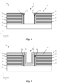
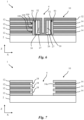
- a method for forming a vertical memory array for a 3D NAND flash memory comprising: forming a layer stack over a substrate, the layer stack comprising an alternating sequence of gate layers and inter-gate spacer layers; forming, along a sidewall surrounding a memory hole in the layer stack, in sequence, a piezoelectric gate layer, a dummy layer and an insulating layer; subjecting the dummy layer to a thermal treatment process adapted to convert the dummy layer into an air gap, wherein the air gap is formed laterally between the piezoelectric gate layer and the insulating liner layer; subsequent to the thermal treatment process, forming, along the insulating liner layer, a charge trap layer, and subsequently, a tunneling oxide layer and a channel layer.
- an improved vertical memory array for a 3D NAND flash memory may be formed.
- a vertical memory array for a 3D NAND flash memory may be formed in which the air gap is located between the piezoelectric gate layer and the insulating liner. This means in practice that the air gap will separate the piezoelectric gate layer and the memory stack of the vertical memory array being formed.
- features of this aspect provide similar advantages as discussed above in relation to the previous aspect. Consequently, said advantages will not be repeated in order to avoid undue repetition.
- the method may further comprise, prior to forming the piezoelectric gate layer: forming recessed areas in the sidewall of the layer stack by laterally etching back the gate layers from the memory hole; wherein the piezoelectric layer is formed selectively in the recessed areas such that a discrete piezoelectric gate layer is formed in each recessed area.
- the dummy layer may be formed selectively on the discrete piezoelectric gate layer in each recessed area.
- a discrete air gap may be formed in each recessed area.
- the dummy layer may be formed of a polymer-comprising material.
- a thermal treatment process e.g. by evaporation, leaving substantially no organic residues in the air gap being formed (although non-polymer traces may remain).
- the insulating liner layer may be deposited at a temperature below a temperature causing conversion of the dummy layer. Accidental conversion of the dummy layer before the air gap is "sealed off" by the liner layer may thus be avoided.
- the insulating liner layer may be formed of a low thermal oxide (LTO).
- LTO low thermal oxide
- a low thermal oxide e.g. LTO SiO 2
- LTO SiO 2 may be reliably deposited without triggering conversion of the dummy layer.
- a thickness of the insulating liner layer may be in a range of 1-4 nm, or 1-2 nm.
- An insulating liner layer in this thickness range allows decomposed components (e.g. vapor-phase components) of the dummy layer, formed upon conversion into air gaps, to exit the (i.e. diffuse) through the liner layer.
- Embodiments of memory cells and memory arrays for a 3D NAND flash memory such as a 3D-Gate-All-Around-NAND (3D GAA NAND), as well as methods for forming such memory array will now be described with reference to the drawings.
- the drawings are only schematic and the relative dimensions of some structures and layers may be exaggerated and not drawn on scale. Rather the dimensions may be adapted for illustrational clarity and to facilitate understanding of the following description.
- the indicated axes X, Y and Z consistently refer to a first horizontal or lateral direction, a second horizontal or lateral direction, and a vertical direction, respectively.
- the terms “horizontal” and “lateral” refer to directions parallel to a supporting substrate of the memory structure.
- the term “vertical” refers to a direction parallel to a normal direction of the substrate, i.e. transverse to the substrate.
- Fig. 1 schematically shows a memory cell 100 for a 3D NAND flash memory according to an embodiment.
- the depicted memory cell 100 includes a gate layer 14 and a channel layer 32.
- a memory stack 40 is arranged between the gate layer 14 and the channel layer 32.
- the memory stack 40 comprises a charge trap layer 27 and a tunneling oxide layer 30.
- the charge trap layer 27 is facing the gate layer 14. That is, the charge trap layer 27 is closer to the gate layer 14 than the tunneling oxide layer 30 is.
- An insulating piezoelectric gate layer 50 is arranged on the gate layer 14.
- the piezoelectric gate layer 50 will hereinafter be referred to as the PZ layer 50.
- the PZ layer 50 and the memory stack 40 are separated by an air gap 52.
- the gate layer 14 may be a nitride-comprising layer, such as a SiN layer, thus forming a sacrificial gate layer 14 intended to be replaced by a replacement metal gate (RMG) stack in subsequent process steps.
- the gate layer 14 may also be a functional gate layer, e.g. a metal layer or a highly doped polysilicon-comprising layer.
- the channel layer 32 may be formed by any suitable channel material conventionally used in the industry for channel layers, typically a semiconductor material such as Si, SiGe or Ge.
- the charge trap layer 27 of the memory stack 40 may comprise or be SiN (i.e. Si 3 N 4 ), or some other oxide material suitable to be used as a charge trap material.
- the charge trap layer 27 may have a thickness in a range of 4 nm to 8 nm.
- the tunneling oxide 30 of the memory stack 40 may be formed of any material conventionally used in the industry for tunneling oxide layers, one non-limiting example being SiON.
- the tunneling oxide 30 may have a thickness in a range of 3 nm to 8 nm.
- the PZ layer 50 may be formed of a suitable insulating piezoelectric material, such as a piezoelectric oxide or nitride.
- the PZ layer 50 may have a thickness of 2 nm to 10 nm. That is, a thickness as seen along the X-axis of Fig. 1 may be 2 nm to 10 nm.
- suitable materials for the PZ layer 50 are HfO 2 , Si doped HfO 2 , ZnO, BN, BaTiO 3 and GaN.
- Such suitable materials for the PZ layer 50 all expand when subjected to a voltage. That is, a thickness of the PZ layer 50 formed of said materials will increase when the PZ layer 50 is subjected to a voltage.
- the thickness of the PZ layer 50 will increase such that the PZ layer 50 expands into the air gap 52 while a thickness of the air gap 52 is decreased correspondingly.
- the PZ layer 50 may have a thickness expansion in a range from 0.2 % to 1.2 % per volt applied to the PZ layer 50.
- the air gap 52 may have a dimension from 0.5 nm to 5 nm. That is, a thickness as seen along the X-axis of Fig. 1 may be 0.5 nm to 5 nm.
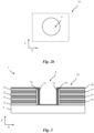
- Fig. 2a-b schematically shows a cross-sectional view, and a top-down view, respectively, of a structure 1 at an initial stage of the method.
- the structure 1 comprises a layer stack 10 representing a precursor or starting structure for the vertical memory array 1 which is to be formed, and as shown in Fig. 7 , to be subjected to the processing steps of the method disclosed in the following.
Landscapes
- Non-Volatile Memory (AREA)
- Semiconductor Memories (AREA)
Priority Applications (3)
| Application Number | Priority Date | Filing Date | Title |
|---|---|---|---|
| EP23218690.8A EP4576977A1 (de) | 2023-12-20 | 2023-12-20 | Speicherzelle für einen 3d-nand-flash-speicher |
| CN202411406636.6A CN120187016A (zh) | 2023-12-20 | 2024-10-10 | 用于3d nand闪存的存储器单元 |
| US18/954,000 US20250212412A1 (en) | 2023-12-20 | 2024-11-20 | Memory cell for a 3d nand flash memory |
Applications Claiming Priority (1)
| Application Number | Priority Date | Filing Date | Title |
|---|---|---|---|
| EP23218690.8A EP4576977A1 (de) | 2023-12-20 | 2023-12-20 | Speicherzelle für einen 3d-nand-flash-speicher |
Publications (1)
| Publication Number | Publication Date |
|---|---|
| EP4576977A1 true EP4576977A1 (de) | 2025-06-25 |
Family
ID=89224722
Family Applications (1)
| Application Number | Title | Priority Date | Filing Date |
|---|---|---|---|
| EP23218690.8A Pending EP4576977A1 (de) | 2023-12-20 | 2023-12-20 | Speicherzelle für einen 3d-nand-flash-speicher |
Country Status (3)
| Country | Link |
|---|---|
| US (1) | US20250212412A1 (de) |
| EP (1) | EP4576977A1 (de) |
| CN (1) | CN120187016A (de) |
Citations (3)
| Publication number | Priority date | Publication date | Assignee | Title |
|---|---|---|---|---|
| US7193283B2 (en) * | 2005-06-20 | 2007-03-20 | Magnachip Semiconductor Ltd. | Flash cell using a piezoelectric effect |
| US20090016095A1 (en) * | 2007-07-09 | 2009-01-15 | Commissariat A L'energie Atomique | Non-volatile sram memory cell equipped with mobile gate transistors and piezoelectric operation |
| US20090196106A1 (en) * | 2006-08-31 | 2009-08-06 | Micron Technology, Inc. | Mem suspended gate non-volatile memory |
-
2023
- 2023-12-20 EP EP23218690.8A patent/EP4576977A1/de active Pending
-
2024
- 2024-10-10 CN CN202411406636.6A patent/CN120187016A/zh active Pending
- 2024-11-20 US US18/954,000 patent/US20250212412A1/en active Pending
Patent Citations (3)
| Publication number | Priority date | Publication date | Assignee | Title |
|---|---|---|---|---|
| US7193283B2 (en) * | 2005-06-20 | 2007-03-20 | Magnachip Semiconductor Ltd. | Flash cell using a piezoelectric effect |
| US20090196106A1 (en) * | 2006-08-31 | 2009-08-06 | Micron Technology, Inc. | Mem suspended gate non-volatile memory |
| US20090016095A1 (en) * | 2007-07-09 | 2009-01-15 | Commissariat A L'energie Atomique | Non-volatile sram memory cell equipped with mobile gate transistors and piezoelectric operation |
Also Published As
| Publication number | Publication date |
|---|---|
| CN120187016A (zh) | 2025-06-20 |
| US20250212412A1 (en) | 2025-06-26 |
Similar Documents
| Publication | Publication Date | Title |
|---|---|---|
| US12408341B2 (en) | Memory arrays, and methods of forming memory arrays | |
| KR102401867B1 (ko) | 메모리 어레이, 및 메모리 어레이를 형성하는 방법 | |
| US7579646B2 (en) | Flash memory with deep quantum well and high-K dielectric | |
| CN110235246A (zh) | 存储器阵列和形成存储器阵列的方法 | |
| CN108447870B (zh) | 3d nand存储器及其制造方法 | |
| JP2005268418A (ja) | 半導体記憶装置及びその製造方法 | |
| US7960267B2 (en) | Method for making a stressed non-volatile memory device | |
| WO2010087265A1 (ja) | 不揮発性半導体記憶装置およびその製造方法 | |
| CN108615733B (zh) | 半导体结构及其形成方法 | |
| JP5306604B2 (ja) | 二値半導体記憶装置 | |
| CN101154632A (zh) | 快闪存储器件的制造方法 | |
| US9337353B2 (en) | Semiconductor device and method for fabricating the same | |
| KR20080001352A (ko) | Sonos 구조를 갖는 반도체 메모리 소자 및 그것의제조 방법 | |
| EP4576977A1 (de) | Speicherzelle für einen 3d-nand-flash-speicher | |
| US20200091179A1 (en) | Semiconductor device and method of fabricating the same | |
| CN1638130A (zh) | 半导体存储器及其制造方法 | |
| CN110010617A (zh) | 一种三维存储器及其制备方法 | |
| CN109449162A (zh) | 3d存储器件的制造方法及3d存储器件 | |
| CN108389864B (zh) | 三维闪存器件的制造方法 | |
| US7749838B2 (en) | Fabricating method of non-volatile memory cell | |
| US20250118547A1 (en) | Methods of forming memory structures for three-dimensional nonvolatile memory | |
| EP4739024A1 (de) | Transistorstruktur, vertikaler nand-flash-speicher und verfahren | |
| KR100762390B1 (ko) | 다층 절연박막 | |
| CN115132734B (zh) | 半导体结构及其形成方法 | |
| KR100771802B1 (ko) | 플래쉬 메모리 소자의 플로팅 게이트 형성 방법 |
Legal Events
| Date | Code | Title | Description |
|---|---|---|---|
| PUAI | Public reference made under article 153(3) epc to a published international application that has entered the european phase |
Free format text: ORIGINAL CODE: 0009012 |
|
| STAA | Information on the status of an ep patent application or granted ep patent |
Free format text: STATUS: THE APPLICATION HAS BEEN PUBLISHED |
|
| AK | Designated contracting states |
Kind code of ref document: A1 Designated state(s): AL AT BE BG CH CY CZ DE DK EE ES FI FR GB GR HR HU IE IS IT LI LT LU LV MC ME MK MT NL NO PL PT RO RS SE SI SK SM TR |
|
| STAA | Information on the status of an ep patent application or granted ep patent |
Free format text: STATUS: REQUEST FOR EXAMINATION WAS MADE |
|
| 17P | Request for examination filed |
Effective date: 20251128 |