EP4579253A1 - Sicherheitsdetektionsverfahren zur verwendung in einer anzeigevorrichtung und zugehörige berührungssteuerungsschaltung sowie berührungs- und anzeigetreiberintegration - Google Patents
Sicherheitsdetektionsverfahren zur verwendung in einer anzeigevorrichtung und zugehörige berührungssteuerungsschaltung sowie berührungs- und anzeigetreiberintegration Download PDFInfo
- Publication number
- EP4579253A1 EP4579253A1 EP24203858.6A EP24203858A EP4579253A1 EP 4579253 A1 EP4579253 A1 EP 4579253A1 EP 24203858 A EP24203858 A EP 24203858A EP 4579253 A1 EP4579253 A1 EP 4579253A1
- Authority
- EP
- European Patent Office
- Prior art keywords
- analog
- display device
- generate
- voltage
- digital
- Prior art date
- Legal status (The legal status is an assumption and is not a legal conclusion. Google has not performed a legal analysis and makes no representation as to the accuracy of the status listed.)
- Pending
Links
Images


Classifications
-
- G—PHYSICS
- G06—COMPUTING OR CALCULATING; COUNTING
- G06F—ELECTRIC DIGITAL DATA PROCESSING
- G06F3/00—Input arrangements for transferring data to be processed into a form capable of being handled by the computer; Output arrangements for transferring data from processing unit to output unit, e.g. interface arrangements
- G06F3/01—Input arrangements or combined input and output arrangements for interaction between user and computer
- G06F3/03—Arrangements for converting the position or the displacement of a member into a coded form
- G06F3/041—Digitisers, e.g. for touch screens or touch pads, characterised by the transducing means
- G06F3/0416—Control or interface arrangements specially adapted for digitisers
-
- G—PHYSICS
- G06—COMPUTING OR CALCULATING; COUNTING
- G06F—ELECTRIC DIGITAL DATA PROCESSING
- G06F3/00—Input arrangements for transferring data to be processed into a form capable of being handled by the computer; Output arrangements for transferring data from processing unit to output unit, e.g. interface arrangements
- G06F3/01—Input arrangements or combined input and output arrangements for interaction between user and computer
- G06F3/03—Arrangements for converting the position or the displacement of a member into a coded form
- G06F3/041—Digitisers, e.g. for touch screens or touch pads, characterised by the transducing means
- G06F3/0412—Digitisers structurally integrated in a display
-
- G—PHYSICS
- G06—COMPUTING OR CALCULATING; COUNTING
- G06F—ELECTRIC DIGITAL DATA PROCESSING
- G06F3/00—Input arrangements for transferring data to be processed into a form capable of being handled by the computer; Output arrangements for transferring data from processing unit to output unit, e.g. interface arrangements
- G06F3/01—Input arrangements or combined input and output arrangements for interaction between user and computer
- G06F3/03—Arrangements for converting the position or the displacement of a member into a coded form
- G06F3/041—Digitisers, e.g. for touch screens or touch pads, characterised by the transducing means
- G06F3/0416—Control or interface arrangements specially adapted for digitisers
- G06F3/04166—Details of scanning methods, e.g. sampling time, grouping of sub areas or time sharing with display driving
-
- G—PHYSICS
- G09—EDUCATION; CRYPTOGRAPHY; DISPLAY; ADVERTISING; SEALS
- G09G—ARRANGEMENTS OR CIRCUITS FOR CONTROL OF INDICATING DEVICES USING STATIC MEANS TO PRESENT VARIABLE INFORMATION
- G09G3/00—Control arrangements or circuits, of interest only in connection with visual indicators other than cathode-ray tubes
- G09G3/006—Electronic inspection or testing of displays and display drivers, e.g. of LED or LCD displays
-
- G—PHYSICS
- G09—EDUCATION; CRYPTOGRAPHY; DISPLAY; ADVERTISING; SEALS
- G09G—ARRANGEMENTS OR CIRCUITS FOR CONTROL OF INDICATING DEVICES USING STATIC MEANS TO PRESENT VARIABLE INFORMATION
- G09G3/00—Control arrangements or circuits, of interest only in connection with visual indicators other than cathode-ray tubes
- G09G3/20—Control arrangements or circuits, of interest only in connection with visual indicators other than cathode-ray tubes for presentation of an assembly of a number of characters, e.g. a page, by composing the assembly by combination of individual elements arranged in a matrix no fixed position being assigned to or needed to be assigned to the individual characters or partial characters
-
- H—ELECTRICITY
- H03—ELECTRONIC CIRCUITRY
- H03M—CODING; DECODING; CODE CONVERSION IN GENERAL
- H03M1/00—Analogue/digital conversion; Digital/analogue conversion
- H03M1/12—Analogue/digital converters
-
- H—ELECTRICITY
- H03—ELECTRONIC CIRCUITRY
- H03M—CODING; DECODING; CODE CONVERSION IN GENERAL
- H03M1/00—Analogue/digital conversion; Digital/analogue conversion
- H03M1/12—Analogue/digital converters
- H03M1/1205—Multiplexed conversion systems
- H03M1/123—Simultaneous, i.e. using one converter per channel but with common control or reference circuits for multiple converters
-
- G—PHYSICS
- G09—EDUCATION; CRYPTOGRAPHY; DISPLAY; ADVERTISING; SEALS
- G09G—ARRANGEMENTS OR CIRCUITS FOR CONTROL OF INDICATING DEVICES USING STATIC MEANS TO PRESENT VARIABLE INFORMATION
- G09G2310/00—Command of the display device
- G09G2310/02—Addressing, scanning or driving the display screen or processing steps related thereto
- G09G2310/0264—Details of driving circuits
- G09G2310/0275—Details of drivers for data electrodes, other than drivers for liquid crystal, plasma or OLED displays, not related to handling digital grey scale data or to communication of data to the pixels by means of a current
-
- G—PHYSICS
- G09—EDUCATION; CRYPTOGRAPHY; DISPLAY; ADVERTISING; SEALS
- G09G—ARRANGEMENTS OR CIRCUITS FOR CONTROL OF INDICATING DEVICES USING STATIC MEANS TO PRESENT VARIABLE INFORMATION
- G09G2330/00—Aspects of power supply; Aspects of display protection and defect management
- G09G2330/02—Details of power systems and of start or stop of display operation
- G09G2330/028—Generation of voltages supplied to electrode drivers in a matrix display other than LCD
-
- G—PHYSICS
- G09—EDUCATION; CRYPTOGRAPHY; DISPLAY; ADVERTISING; SEALS
- G09G—ARRANGEMENTS OR CIRCUITS FOR CONTROL OF INDICATING DEVICES USING STATIC MEANS TO PRESENT VARIABLE INFORMATION
- G09G2330/00—Aspects of power supply; Aspects of display protection and defect management
- G09G2330/12—Test circuits or failure detection circuits included in a display system, as permanent part thereof
-
- G—PHYSICS
- G09—EDUCATION; CRYPTOGRAPHY; DISPLAY; ADVERTISING; SEALS
- G09G—ARRANGEMENTS OR CIRCUITS FOR CONTROL OF INDICATING DEVICES USING STATIC MEANS TO PRESENT VARIABLE INFORMATION
- G09G2354/00—Aspects of interface with display user
Definitions
- the present disclosure relates to safety detection of integrated circuits, and more particularly, to a safety detection method and related touch control circuit and touch and display driver integration.
- Automotive integrated circuits are custom-designed for specific applications within automotive electronic systems. These ICs are engineered to meet the stringent requirements of automotive applications, such as high reliability, durability, and compliance with automotive safety standards like ISO 26262. Commonly, automotive ICs serve a variety of functions in vehicle systems, including engine control units (ECUs), sensor interfaces, infotainment systems, and advanced driver assistance systems (ADAS). Given the high demands for reliability and durability, the ISO 26262 standard outlines four safety levels: ASIL-A, ASII,-B, ASIL-C, and ASIL-D. Generally, automotive components such as the dashboard, passenger-side panel, rearview mirrors, rear-seat entertainment devices, and door handles are required to meet at least the ASII,-B safety level.
- ECUs engine control units
- ADAS advanced driver assistance systems
- SPFM single point fault metric
- LFM latent fault metric
- source driver circuitry is significant in terms of both the number of transistors and the proportion of circuit area within the TDDI IC. Without dedicated safety detection circuits designed for the source driver circuitry, it is impossible to meet the 90% single point fault requirement.
- the present invention introduces a novel safety detection method along with an associated touch control circuit.
- analog-to-digital converters within a touch control circuit of the TDDI IC are utilized to implement safety detection for the source driver circuitry. Since these analog-to-digital converters are idle during non-touch sensing periods, their use in the safety detection of the source driver does not disrupt the normal operation of the touch control circuit.
- the safety detection method and associated touch control circuit of the present invention can also be applied to other analog circuitry (such as voltage regulators and charge pump converters) in automotive display devices to monitor their output voltages for safety. This effectively eliminates potential errors and abnormal output voltages that may arise from various causes in these circuits. Consequently, the present invention significantly enhances the reliability of automotive TDDI IC, thereby substantially improving the safety of vehicle systems.
- the touch control circuit includes: a plurality of analog-to-digital converters and a controller.
- Each of the analog-to-digital converters is coupled to at least one of a plurality of touch sensing electrodes and at least one of a plurality of source drivers of the display device.
- At least one of the analog-to-digital converters is configured to generate a first measured digital code according to an output voltage outputted by at the least one of the source drivers.
- the controller is coupled to the analog-to-digital converters, and configured to compare the first measured digital code with an input digital code that the output voltage of the at the least one of the source drivers corresponds to, thereby to generate a first safety detection result regarding the at least one of the source drivers.
- the safety detection method comprises: providing a touch control circuit including a plurality of analog-to-digital converters, each coupled to at least one of a plurality of touch sensing electrodes and at least one of a plurality of source drivers of the display device; utilizing at least one of the analog-to-digital converters to generate a first measured digital code according to an output voltage outputted by at the least one of the source drivers; and comparing the first measured digital code with an input digital code that the output voltage of the at the least one of the source drivers corresponds to, thereby to generate a first safety detection result regarding the at least one of the source drivers.
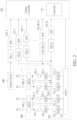
- a display device 10 is a touch-enabled display and comprises a display panel 300 and a touch and display driver integration integrated circuit (TDDI IC) 50.
- the display device 10 is controlled by the TDDI IC 50, which includes a touch control circuit 100, a display driving circuit 200, and a timing controller 400.
- the touch control circuit 100 is configured to detect touch inputs on a display panel 300 of the display device 10, facilitating user interaction with the display device 10. This detection involves processing signals corresponding to touch events, such as taps or swipes, executed on the surface of the display panel 300.
- the display driving circuit 200 is configured to control pixel circuits within the display panel 300. Its function is to accurately render visual content, like videos or images, by manipulating pixel behavior, such as color and brightness, according to the video/image data and timing signals provided by the timing controller 400.
- the timing controller 400 is configured to synchronize operations of the touch control circuit 100 and the display driving circuit 200, thereby to ensure that touch detection and display rendering processes are perfectly coordinated.
- the display panel 300 incorporates a sophisticated arrangement of electrodes for pixel control and touch sensing. Specifically, source electrodes SO-SP and gate electrodes G0-GQ that are strategically positioned on the display panel 300, where the source electrodes SO-SP are configured to supply pixel driving voltages to the pixel circuits, and the gate electrodes G0-GQ are configured to control the timing of pixel driving voltages supplying to individual pixel circuits.
- the source electrodes SO-SP and gate electrodes G0-GQ are primarily controlled by the display driving circuit 200.
- the display panel 300 also incorporates touch driving electrodes TD0-TDR and touch sensing electrodes TS0-TST.
- the touch driving electrodes TD0-TDR are configured to emit electric fields, while the touch sensing electrodes TS0-TST detect changes in electric fields caused by a user's touch. This arrangement enables the touch control circuit 100 to accurately detect and interpret touch inputs across the surface of the display panel 300.
- the specific arrangements of the source electrodes SO-SP, the gate electrodes G0-GQ, the touch driving electrodes TD0-TDR, and the touch sensing electrodes TS0-TST as shown in FIG. 1 are exemplary and not intended to limit the scope of the present invention. They are merely illustrative of one possible configuration among many that could achieve the desired functionality within the scope of the present invention.
- the display driving circuit 200 comprises a latching circuit 210, a plurality of digital-to-analog converters 220_1-220_N, a plurality of source drivers 230_1-230_N.
- the latching circuit 210 comprises a first latch 211 and a plurality of second latches 212_1-212_N.
- the timing controller 400 is configured to send image data to be displayed to the first latch 211 of the latching circuit 210.
- each of the second latches 212_1-212_N receives and outputs a data segment (e.g., data pertaining to RGB sub-pixels of the horizontal line) of the data of the line of the image to one of the digital-to-analog converters 220_1-220_N.
- each of the digital-to-analog converters 220_1-220_N is configured to convert its received data segment into a converted analog voltage and forward it to a corresponding one of the source drivers 230_1-230_N.
- each of the source drivers 230_1-230_N applies its received converted analog voltage to a corresponding one of the source electrodes SO-SP (as a pixel driving voltage), for manipulating respective pixel circuits on the display panel 300, thereby displaying the image line by line.
- the touch control circuit 100 comprises a plurality of voltage conversion circuit 110_1-110_K (which can be optional), a plurality of analog-to-digital converters 120_1-120_K and a controller 130.
- the analog-to-digital converters 120_1-120_K is configured to respectively convert analog voltages sensed on the touch sensing electrodes TS0-TST, which are indicative of touch interactions on the display panel 300, to generate digital touch sensed signals (which can be in form of digital codes).
- the generated touch sensed signals encapsulate the intensity, location, and other relevant touch attributes detected by the touch sensing electrodes TS0-TST.
- these digital touch sensed signals are then relayed to the controller 130.
- the controller 130 is configured to interpret these digital touch sensed signals to ascertain the presence, nature, and specifics of one or more touch events on the display panel 300.
- the controller 130 analyzes the incoming data to distinguish between various touch gestures, thereby enabling accurate and responsive touch interaction with the display device 10.
- outputs of the source drivers 230_1-230_N are coupled to the touch control circuit 100 through multiplexers 500_1-500_J and switches.
- outputs voltages of the source drivers 230_1-230_N can be initially directed to the voltage conversion circuits 110_1-110_K, which are capable of adjusting (shifting) the output voltages to transferred voltages whose levels are suitable for an input voltage range of the analog-to-digital converters 120_1-120_K.
- this routing through the voltage conversion circuits 110_1-110_K is not the only possible configuration as per the scope of the present invention.
- the output voltages of the source drivers 230_1-230_N can be directly fed into the analog-to-digital converters 120_1-120_K, bypassing any voltage level adjustment.
- the primary objective of the voltage conversion circuits 110_1-110_K is to modify the output voltages of the source drivers 230_1-230_N such that the output voltages of the source drivers 230_1-230_N can align with the input voltage range of the analog-to-digital converters 120_1-120_K.
- This input voltage range is defined as a range of voltage levels that the analog-to-digital converters 120_1-120_K can precisely interpret.
- the input voltage range of the analog-to-digital converters 120_1-120_K is limited.
- the function of the voltage conversion circuits 110_1-110_K is to adjust/shift any input voltage that either exceeds or falls short of the input voltage range of the analog-to-digital converters 120_1-120_K. This adjustment ensures that the voltage falls within the range that the analog-to-digital converters 120_1-120_K can accurately process, thereby guaranteeing reliable and accurate digital conversion of the input signals.
- the analog-to-digital converters 120_1-120_K of the touch control circuit 100 are configured to convert either the output voltages of the source drivers 230_1-230_N or the transferred voltages into corresponding measured digital codes.
- the controller 130 is configured to perform comparative analysis between the measured digital codes and predefined input digital codes. Specifically, the input digital codes are data segments of the line of the image that are respectively and individually fed to the each of the digital-to-analog converters 220_1-220_N.
- the controller 130 If an input digital code is not consistent with a measured digital code, this indicates a potential malfunction in either a corresponding one of the source drivers 230_1-230_N or a corresponding one of the digital-to-analog converters 220_1-220_N since the input digital code inputted to each of the digital-to-analog converters 220_1-220_N should be consistent with the measured digital code generated by a corresponding one of the analog-to-digital converters 120_1-120_K.
- the controller 130 generates a safety detection result indicative of whether each of source drivers 230_1-230 N operates properly without any faults based on the measured digital codes and the input digital codes.
- the controller 130 could be integrated as a part of the timing controller 400.
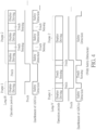
- the safety detection provided by the present invention is based on a time-sharing utilization on the analog-to-digital converters 120_1-120_K. Please refer to FIG. 3 and FIG. 4 for further understandings.
- the analog-to-digital converters 120_1-120_K is trigger/enabled to convert voltages sensed on the touch sensing electrodes during touch sensing periods in a long-V or a long-H mode, where long-V mode is inter-frame touch driving, which means touch sensing operations are performed between the two display frame periods (i.e., a blanking period) and long-H mode is intra-frame touch driving, which means touch sensing operations are inserted and performed within one display frame period.
- the analog-to-digital converters 120_1-120_K is utilized to facilitate the safety detection during display driving periods of the TDDI IC 50 and the display device 10 since touch sensing operations only need to be performed during touch sensing periods of the TDDI IC 50 and the display device 10 and therefore the analog-to-digital converters 120_1-120_K is available for other purposes during non-touch sensing periods.
- the analog-to-digital converters 120_1-120_K can be enabled/triggered to facilitate the safety detection during non-touch sensing periods (e.g., display driving periods or porch periods) of the TDDI IC 50 and the display device 10.
- the number of the source drivers 230_1-230 N may be not identical to the number of the analog-to-digital converters 120_1-120_K of the touch control circuit 100, and it is often the case that there are more source drivers 230_1-230 than the analog-to-digital converters 120_1-120_K of the touch control circuit 100. Given the limited number of the analog-to-digital converters 120_1-120_K available, it is not feasible to conduct the safety detection on all the source drivers 230_1-230_N simultaneously. Therefore, safety detection may be performed in batches in some embodiments of the present invention. That is, the safety detection is performed on only a portion of the source drivers 230_1-230_N during a single one safety detection period.
- the safety detection on a first portion of source drivers 230_1-230_N can be performed during a display driving period of displaying a first frame on the display panel 300, while the safety detection on a second portion of source drivers 230_1-230_N can be performed during a display driving period of displaying a second frame on the display panel 300.
- the safety detection mechanism provided by the present invention can be further applied to one or more analog circuits 600 of the display device 10.
- the one or more analog circuits 600 could comprise at least one of a voltage regulator (e.g., low-dropout regulator (LDO)), a charge pump, a gamma voltage regulator and a gate voltage generator of the display device 10.
- LDO low-dropout regulator
- the output voltages of the one or more analog circuits 600 may either exceed or fall below the input voltage range of the analog-to-digital converters 120_1-120_K, these output voltages might require conversion to appropriate levels before being read and converted by the analog-to-digital converters 120_1-120_K. However, not all the output voltages of the one or more analog circuits 600 necessitate such conversion. In certain scenarios, the output voltages of the one or more analog circuits 600 can be directly read and converted by the analog-to-digital converters 120_1-120_K without any prior adjustment to transferred voltages.
- the output voltages of the one or more analog circuits 600 or their corresponding transferred voltages are converted into measured digital codes by the analog-to-digital converters 120_1-120_K.
- the converted measured digital codes would be compared with a target digital code range.
- the target digital code range indicates a predefine range of the output voltages of the one or more analog circuits 600. If the measured digital codes exceed or fall below the predefine range of the output voltages of the one or more analog circuits 600, this indicates a potential malfunction in the one or more analog circuits 600.
- the controller 130 generates a safety detection result indicative of whether each of the one or more analog circuits 600 operates properly without any faults.
- the safety detection on the one or more analog circuits 600 can be performed during any non-touch sensing periods (e.g., display driving periods or porch periods) of the TDDI IC 50 and the display device 10.
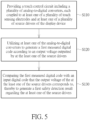
- FIG. 5 illustrates a safety detection method for use in a display device according to one embodiment of the present invention.
- the method of the present invention includes the following simplified flow: Step S110: providing a touch control circuit including a plurality of analog-to-digital converters, each coupled to at least one of a plurality of touch sensing electrodes and at least one of a plurality of source drivers of the display device; Step S120: utilizing at least one of the analog-to-digital converters to generate a first measured digital code according to an output voltage outputted by at the least one of the source drivers; and Step S130: comparing the first measured digital code with an input digital code that the output voltage of the at the least one of the source drivers corresponds to, thereby to generate a first safety detection result regarding the at least one of the source drivers.
Landscapes
- Engineering & Computer Science (AREA)
- Theoretical Computer Science (AREA)
- General Engineering & Computer Science (AREA)
- Physics & Mathematics (AREA)
- General Physics & Mathematics (AREA)
- Human Computer Interaction (AREA)
- Computer Hardware Design (AREA)
- Control Of Indicators Other Than Cathode Ray Tubes (AREA)
- Control Of El Displays (AREA)
Applications Claiming Priority (1)
| Application Number | Priority Date | Filing Date | Title |
|---|---|---|---|
| US18/399,732 US12131678B1 (en) | 2023-12-29 | 2023-12-29 | Safety detection method for use in display device and related touch control circuit and touch and display driver integration |
Publications (1)
| Publication Number | Publication Date |
|---|---|
| EP4579253A1 true EP4579253A1 (de) | 2025-07-02 |
Family
ID=92966983
Family Applications (1)
| Application Number | Title | Priority Date | Filing Date |
|---|---|---|---|
| EP24203858.6A Pending EP4579253A1 (de) | 2023-12-29 | 2024-10-01 | Sicherheitsdetektionsverfahren zur verwendung in einer anzeigevorrichtung und zugehörige berührungssteuerungsschaltung sowie berührungs- und anzeigetreiberintegration |
Country Status (4)
| Country | Link |
|---|---|
| US (1) | US12131678B1 (de) |
| EP (1) | EP4579253A1 (de) |
| CN (1) | CN120233899A (de) |
| TW (1) | TWI898890B (de) |
Citations (7)
| Publication number | Priority date | Publication date | Assignee | Title |
|---|---|---|---|---|
| US5787114A (en) * | 1996-01-17 | 1998-07-28 | Lsi Logic Corporation | Loop-back test system and method |
| WO2008137980A1 (en) * | 2007-05-08 | 2008-11-13 | Synaptics Incorporated | Production testing of a capacitive touch sensing device |
| CN102207535A (zh) * | 2010-03-30 | 2011-10-05 | 上海摩波彼克半导体有限公司 | 对含adc和dac的模拟基带芯片自动测试的电路结构及方法 |
| JP2012044406A (ja) * | 2010-08-18 | 2012-03-01 | Kawasaki Microelectronics Inc | 半導体集積回路およびそのテスト方法 |
| CN102998611A (zh) * | 2011-09-09 | 2013-03-27 | 中国航天科工集团第三研究院第八三五八研究所 | 一种对包含adc和dac的电路的快速检测方法 |
| US20180182333A1 (en) * | 2016-12-23 | 2018-06-28 | Silicon Works Co., Ltd. | Panel-driving device and display device |
| US20220256139A1 (en) * | 2020-02-26 | 2022-08-11 | Samsung Electronics Co., Ltd. | Image sensing device and operating the same |
Family Cites Families (12)
| Publication number | Priority date | Publication date | Assignee | Title |
|---|---|---|---|---|
| US7250940B2 (en) * | 2003-12-31 | 2007-07-31 | Symbol Technologies, Inc. | Touch screen apparatus and method therefore |
| TWI285358B (en) * | 2004-07-30 | 2007-08-11 | Sunplus Technology Co Ltd | TFT LCD source driver with built in test circuit and method for testing the same |
| KR20070040505A (ko) * | 2005-10-12 | 2007-04-17 | 삼성전자주식회사 | 표시 장치 및 이의 검사 방법 |
| DE102009046177A1 (de) * | 2008-10-30 | 2010-06-10 | Samsung Electronics Co., Ltd., Suwon | Berührungsdatengenerator |
| US8358256B2 (en) * | 2008-11-17 | 2013-01-22 | Global Oled Technology Llc | Compensated drive signal for electroluminescent display |
| KR102127902B1 (ko) * | 2013-10-14 | 2020-06-30 | 삼성디스플레이 주식회사 | 표시 장치 및 표시 장치의 구동 방법 |
| KR101623776B1 (ko) * | 2013-12-09 | 2016-06-07 | 엘지디스플레이 주식회사 | 터치 디스플레이 드라이버 집적회로 및 터치 표시장치 |
| CN110264925B (zh) * | 2019-06-11 | 2021-11-05 | 惠科股份有限公司 | 显示装置及其短路检测方法 |
| CN112394830B (zh) * | 2019-08-15 | 2024-07-16 | 联咏科技股份有限公司 | 触摸模拟前端电路及其触摸显示设备 |
| KR102713410B1 (ko) * | 2019-10-02 | 2024-10-02 | 엘지디스플레이 주식회사 | 표시 장치 및 표시 장치 구동 방법 |
| KR20240040895A (ko) * | 2022-09-22 | 2024-03-29 | 주식회사 엘엑스세미콘 | 데이터구동회로 및 이를 포함하는 디스플레이구동회로 |
| KR20240121526A (ko) * | 2023-02-02 | 2024-08-09 | 엘지디스플레이 주식회사 | 데이터 구동 회로 및 이를 포함하는 표시 장치 |
-
2023
- 2023-12-29 US US18/399,732 patent/US12131678B1/en active Active
-
2024
- 2024-09-29 CN CN202411367964.XA patent/CN120233899A/zh active Pending
- 2024-10-01 EP EP24203858.6A patent/EP4579253A1/de active Pending
- 2024-10-23 TW TW113140285A patent/TWI898890B/zh active
Patent Citations (7)
| Publication number | Priority date | Publication date | Assignee | Title |
|---|---|---|---|---|
| US5787114A (en) * | 1996-01-17 | 1998-07-28 | Lsi Logic Corporation | Loop-back test system and method |
| WO2008137980A1 (en) * | 2007-05-08 | 2008-11-13 | Synaptics Incorporated | Production testing of a capacitive touch sensing device |
| CN102207535A (zh) * | 2010-03-30 | 2011-10-05 | 上海摩波彼克半导体有限公司 | 对含adc和dac的模拟基带芯片自动测试的电路结构及方法 |
| JP2012044406A (ja) * | 2010-08-18 | 2012-03-01 | Kawasaki Microelectronics Inc | 半導体集積回路およびそのテスト方法 |
| CN102998611A (zh) * | 2011-09-09 | 2013-03-27 | 中国航天科工集团第三研究院第八三五八研究所 | 一种对包含adc和dac的电路的快速检测方法 |
| US20180182333A1 (en) * | 2016-12-23 | 2018-06-28 | Silicon Works Co., Ltd. | Panel-driving device and display device |
| US20220256139A1 (en) * | 2020-02-26 | 2022-08-11 | Samsung Electronics Co., Ltd. | Image sensing device and operating the same |
Also Published As
| Publication number | Publication date |
|---|---|
| TW202526871A (zh) | 2025-07-01 |
| TWI898890B (zh) | 2025-09-21 |
| CN120233899A (zh) | 2025-07-01 |
| US12131678B1 (en) | 2024-10-29 |
Similar Documents
| Publication | Publication Date | Title |
|---|---|---|
| US11423849B2 (en) | Display panel having a voltage compensation circuit | |
| US9501997B2 (en) | Gate driver and display apparatus | |
| KR101349665B1 (ko) | 터치 스크린 일체형 표시장치 | |
| JP6955017B2 (ja) | 液晶表示装置、映像表示システムおよび車両 | |
| CN109243355B (zh) | 伽马电压校正电路、方法及显示装置 | |
| US9342199B2 (en) | Touch detection device, display device with touch detection function, and electronic apparatus | |
| EP3163562B1 (de) | Pixelschaltung, anzeigetafel und anzeigevorrichtung | |
| KR101747263B1 (ko) | 드라이버ic 및 이를 이용한 표시장치 | |
| JP5599040B2 (ja) | 基準電圧生成回路、電源装置、液晶表示装置 | |
| US10991295B2 (en) | Display driver, electro-optical device, electronic apparatus, and mobile body | |
| US20180218707A1 (en) | Gate voltage driving device, method, driving circuit, and liquid crystal display panel | |
| CN104183222B (zh) | 显示装置 | |
| CN108172155A (zh) | 一种检测装置及检测方法 | |
| US12013740B2 (en) | Touch display device and power supply control method | |
| US11132971B2 (en) | Voltage supply circuit, liquid crystal device, electronic apparatus, and mobile body | |
| EP4579253A1 (de) | Sicherheitsdetektionsverfahren zur verwendung in einer anzeigevorrichtung und zugehörige berührungssteuerungsschaltung sowie berührungs- und anzeigetreiberintegration | |
| WO2020258494A1 (zh) | 显示驱动方法、显示面板和显示装置 | |
| US10650724B2 (en) | Display device and driving method thereof | |
| US20140192096A1 (en) | Liquid crystal display device | |
| JP2017125920A (ja) | 高解析ディスプレイ及びそのドライバーチップ | |
| US20230121015A1 (en) | Gate driving method, gate driving circuit and display device | |
| US20230005401A1 (en) | Data driving circuit, method for detecting noise of display signal, and display apparatus | |
| US10410593B2 (en) | Display panel driving apparatus and display apparatus having the same | |
| US20170372652A1 (en) | Power supply circuit, circuit device, display device, and electronic apparatus | |
| US7916132B2 (en) | Systems for displaying images and related methods |
Legal Events
| Date | Code | Title | Description |
|---|---|---|---|
| PUAI | Public reference made under article 153(3) epc to a published international application that has entered the european phase |
Free format text: ORIGINAL CODE: 0009012 |
|
| STAA | Information on the status of an ep patent application or granted ep patent |
Free format text: STATUS: REQUEST FOR EXAMINATION WAS MADE |
|
| 17P | Request for examination filed |
Effective date: 20250508 |
|
| AK | Designated contracting states |
Kind code of ref document: A1 Designated state(s): AL AT BE BG CH CY CZ DE DK EE ES FI FR GB GR HR HU IE IS IT LI LT LU LV MC ME MK MT NL NO PL PT RO RS SE SI SK SM TR |
|
| GRAP | Despatch of communication of intention to grant a patent |
Free format text: ORIGINAL CODE: EPIDOSNIGR1 |
|
| STAA | Information on the status of an ep patent application or granted ep patent |
Free format text: STATUS: GRANT OF PATENT IS INTENDED |
|
| INTG | Intention to grant announced |
Effective date: 20251020 |
|
| GRAS | Grant fee paid |
Free format text: ORIGINAL CODE: EPIDOSNIGR3 |
|
| GRAA | (expected) grant |
Free format text: ORIGINAL CODE: 0009210 |
|
| STAA | Information on the status of an ep patent application or granted ep patent |
Free format text: STATUS: THE PATENT HAS BEEN GRANTED |