EP4579743A1 - Amplificateur de puissance à trajets multiples avec condensateur pour compenser un couplage entre des trajets d'amplificateur - Google Patents
Amplificateur de puissance à trajets multiples avec condensateur pour compenser un couplage entre des trajets d'amplificateur Download PDFInfo
- Publication number
- EP4579743A1 EP4579743A1 EP23307397.2A EP23307397A EP4579743A1 EP 4579743 A1 EP4579743 A1 EP 4579743A1 EP 23307397 A EP23307397 A EP 23307397A EP 4579743 A1 EP4579743 A1 EP 4579743A1
- Authority
- EP
- European Patent Office
- Prior art keywords
- capacitor
- input
- amplifier
- transistor
- circuit
- Prior art date
- Legal status (The legal status is an assumption and is not a legal conclusion. Google has not performed a legal analysis and makes no representation as to the accuracy of the status listed.)
- Pending
Links
Images



Classifications
-
- H—ELECTRICITY
- H03—ELECTRONIC CIRCUITRY
- H03F—AMPLIFIERS
- H03F1/00—Details of amplifiers with only discharge tubes, only semiconductor devices or only unspecified devices as amplifying elements
- H03F1/02—Modifications of amplifiers to raise the efficiency, e.g. gliding Class A stages, use of an auxiliary oscillation
- H03F1/0205—Modifications of amplifiers to raise the efficiency, e.g. gliding Class A stages, use of an auxiliary oscillation in transistor amplifiers
- H03F1/0288—Modifications of amplifiers to raise the efficiency, e.g. gliding Class A stages, use of an auxiliary oscillation in transistor amplifiers using a main and one or several auxiliary peaking amplifiers whereby the load is connected to the main amplifier using an impedance inverter, e.g. Doherty amplifiers
-
- H—ELECTRICITY
- H03—ELECTRONIC CIRCUITRY
- H03F—AMPLIFIERS
- H03F1/00—Details of amplifiers with only discharge tubes, only semiconductor devices or only unspecified devices as amplifying elements
- H03F1/08—Modifications of amplifiers to reduce detrimental influences of internal impedances of amplifying elements
- H03F1/083—Modifications of amplifiers to reduce detrimental influences of internal impedances of amplifying elements in transistor amplifiers
- H03F1/086—Modifications of amplifiers to reduce detrimental influences of internal impedances of amplifying elements in transistor amplifiers with FET's
-
- H—ELECTRICITY
- H03—ELECTRONIC CIRCUITRY
- H03F—AMPLIFIERS
- H03F1/00—Details of amplifiers with only discharge tubes, only semiconductor devices or only unspecified devices as amplifying elements
- H03F1/56—Modifications of input or output impedances, not otherwise provided for
- H03F1/565—Modifications of input or output impedances, not otherwise provided for using inductive elements
-
- H—ELECTRICITY
- H03—ELECTRONIC CIRCUITRY
- H03F—AMPLIFIERS
- H03F3/00—Amplifiers with only discharge tubes or only semiconductor devices as amplifying elements
- H03F3/189—High-frequency amplifiers, e.g. radio frequency amplifiers
- H03F3/19—High-frequency amplifiers, e.g. radio frequency amplifiers with semiconductor devices only
- H03F3/195—High-frequency amplifiers, e.g. radio frequency amplifiers with semiconductor devices only in integrated circuits
-
- H—ELECTRICITY
- H03—ELECTRONIC CIRCUITRY
- H03F—AMPLIFIERS
- H03F3/00—Amplifiers with only discharge tubes or only semiconductor devices as amplifying elements
- H03F3/20—Power amplifiers, e.g. Class B amplifiers, Class C amplifiers
-
- H—ELECTRICITY
- H03—ELECTRONIC CIRCUITRY
- H03F—AMPLIFIERS
- H03F3/00—Amplifiers with only discharge tubes or only semiconductor devices as amplifying elements
- H03F3/20—Power amplifiers, e.g. Class B amplifiers, Class C amplifiers
- H03F3/21—Power amplifiers, e.g. Class B amplifiers, Class C amplifiers with semiconductor devices only
- H03F3/213—Power amplifiers, e.g. Class B amplifiers, Class C amplifiers with semiconductor devices only in integrated circuits
-
- H—ELECTRICITY
- H03—ELECTRONIC CIRCUITRY
- H03F—AMPLIFIERS
- H03F3/00—Amplifiers with only discharge tubes or only semiconductor devices as amplifying elements
- H03F3/20—Power amplifiers, e.g. Class B amplifiers, Class C amplifiers
- H03F3/24—Power amplifiers, e.g. Class B amplifiers, Class C amplifiers of transmitter output stages
- H03F3/245—Power amplifiers, e.g. Class B amplifiers, Class C amplifiers of transmitter output stages with semiconductor devices only
-
- H—ELECTRICITY
- H10—SEMICONDUCTOR DEVICES; ELECTRIC SOLID-STATE DEVICES NOT OTHERWISE PROVIDED FOR
- H10W—GENERIC PACKAGES, INTERCONNECTIONS, CONNECTORS OR OTHER CONSTRUCTIONAL DETAILS OF DEVICES COVERED BY CLASS H10
- H10W44/00—Electrical arrangements for controlling or matching impedance
- H10W44/20—Electrical arrangements for controlling or matching impedance at high-frequency [HF] or radio frequency [RF]
-
- H—ELECTRICITY
- H03—ELECTRONIC CIRCUITRY
- H03F—AMPLIFIERS
- H03F2200/00—Indexing scheme relating to amplifiers
- H03F2200/114—Indexing scheme relating to amplifiers the amplifier comprising means for electro-magnetic interference [EMI] protection
-
- H—ELECTRICITY
- H03—ELECTRONIC CIRCUITRY
- H03F—AMPLIFIERS
- H03F2200/00—Indexing scheme relating to amplifiers
- H03F2200/222—A circuit being added at the input of an amplifier to adapt the input impedance of the amplifier
-
- H—ELECTRICITY
- H03—ELECTRONIC CIRCUITRY
- H03F—AMPLIFIERS
- H03F2200/00—Indexing scheme relating to amplifiers
- H03F2200/451—Indexing scheme relating to amplifiers the amplifier being a radio frequency amplifier
-
- H—ELECTRICITY
- H10—SEMICONDUCTOR DEVICES; ELECTRIC SOLID-STATE DEVICES NOT OTHERWISE PROVIDED FOR
- H10W—GENERIC PACKAGES, INTERCONNECTIONS, CONNECTORS OR OTHER CONSTRUCTIONAL DETAILS OF DEVICES COVERED BY CLASS H10
- H10W44/00—Electrical arrangements for controlling or matching impedance
- H10W44/20—Electrical arrangements for controlling or matching impedance at high-frequency [HF] or radio frequency [RF]
- H10W44/203—Electrical connections
- H10W44/206—Wires
-
- H—ELECTRICITY
- H10—SEMICONDUCTOR DEVICES; ELECTRIC SOLID-STATE DEVICES NOT OTHERWISE PROVIDED FOR
- H10W—GENERIC PACKAGES, INTERCONNECTIONS, CONNECTORS OR OTHER CONSTRUCTIONAL DETAILS OF DEVICES COVERED BY CLASS H10
- H10W44/00—Electrical arrangements for controlling or matching impedance
- H10W44/20—Electrical arrangements for controlling or matching impedance at high-frequency [HF] or radio frequency [RF]
- H10W44/226—Electrical arrangements for controlling or matching impedance at high-frequency [HF] or radio frequency [RF] for HF amplifiers
- H10W44/234—Arrangements for impedance matching
-
- H—ELECTRICITY
- H10—SEMICONDUCTOR DEVICES; ELECTRIC SOLID-STATE DEVICES NOT OTHERWISE PROVIDED FOR
- H10W—GENERIC PACKAGES, INTERCONNECTIONS, CONNECTORS OR OTHER CONSTRUCTIONAL DETAILS OF DEVICES COVERED BY CLASS H10
- H10W44/00—Electrical arrangements for controlling or matching impedance
- H10W44/20—Electrical arrangements for controlling or matching impedance at high-frequency [HF] or radio frequency [RF]
- H10W44/241—Electrical arrangements for controlling or matching impedance at high-frequency [HF] or radio frequency [RF] for passive devices or passive elements
-
- H—ELECTRICITY
- H10—SEMICONDUCTOR DEVICES; ELECTRIC SOLID-STATE DEVICES NOT OTHERWISE PROVIDED FOR
- H10W—GENERIC PACKAGES, INTERCONNECTIONS, CONNECTORS OR OTHER CONSTRUCTIONAL DETAILS OF DEVICES COVERED BY CLASS H10
- H10W44/00—Electrical arrangements for controlling or matching impedance
- H10W44/20—Electrical arrangements for controlling or matching impedance at high-frequency [HF] or radio frequency [RF]
- H10W44/241—Electrical arrangements for controlling or matching impedance at high-frequency [HF] or radio frequency [RF] for passive devices or passive elements
- H10W44/243—Electrical arrangements for controlling or matching impedance at high-frequency [HF] or radio frequency [RF] for passive devices or passive elements for decoupling, e.g. bypass capacitors
Definitions
- This present disclosure relates, in general, to multiple-path amplifiers, and in particular to compensating for coupling between amplifiers of a multiple-path power amplifier component.
- the subject disclosure describes, among other things, illustrative embodiments for compensating for coupling (e.g., parasitic or inductive coupling) between paths of a multiple-path power amplifier circuit.
- coupling e.g., parasitic or inductive coupling
- One or more of the exemplary embodiments may include, in whole or in part, a first amplifier path that includes a first output, a first transistor, and a first wire coupled between the first output and a first terminal of the first transistor, a second amplifier path that includes a second output, a second transistor, and a second wire coupled between the second output and a first terminal of the second transistor, and a capacitor with a first terminal coupled to the first output and a second terminal coupled to the second output, wherein the capacitor is configured to compensate for a coupling between the first wire and the second wire.
- One or more of the exemplary embodiments may include, in whole or in part, a radio frequency (RF) input node, a RF output node, a power splitter configured to split an input RF signal received at the RF input node and divide power of the input RF signal into a carrier portion of the input RF signal and a peaking portion of the input RF signal, wherein the carrier portion traverses a first path that includes a first transistor and the peaking portion traverses a second path that includes a second transistor, and a first capacitor with a first terminal coupled to the first path and a second terminal coupled to the second path, the first capacitor compensating for parasitic coupling between first wirebonds of the first path and second wirebonds of the second path.
- RF radio frequency
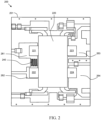
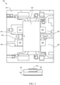
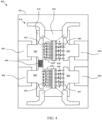
- the Doherty power amplifier 100 may be supported by a substrate 101, such as a printed circuit board (PCB) (e.g., PCB 201, 301, 401, FIGs 2-4 ).
- a substrate 101 such as a printed circuit board (PCB) (e.g., PCB 201, 301, 401, FIGs 2-4 ).
- various components of the Doherty power amplifier 100 may be housed in a packaged semiconductor device 120 (e.g., device 220, 320, 420, FIGs 2-4 ), which may be mounted on the substrate 101.
- PCB printed circuit board
- Doherty amplifier 100 includes an RF input node 102 (e.g., a first coaxial RF connector), an RF output node 104 (e.g., a second coaxial RF connector), a signal splitter 110, a carrier amplification path 130 (generally, a "first amplification path”), a peaking amplification path 150 (generally, a "second amplification path”), a combining node 170, and an output impedance transformer 190, in an embodiment.
- Doherty power amplifier 100 is considered to be a "two-way" Doherty power amplifier, which includes one carrier amplification path 130 and one peaking amplification path 150. In other embodiments, more than one peaking amplification path may be implemented in parallel with the first peaking amplification path 150 to produce an N-way Doherty power amplifier, where N>2.
- the RF input node 102 When incorporated into a larger RF system, the RF input node 102 is coupled to an RF signal source (not shown), and the RF output node 104 is coupled to a load 106 (e.g., an antenna or other load).
- the RF signal source provides an input RF signal, which is an analog signal that includes spectral energy that typically is centered around one or more carrier frequencies.
- the Doherty amplifier 100 is configured to amplify the input RF signal, and to produce an amplified RF signal at the RF output node 104.
- power splitter 110 may be implemented on the substrate 101.
- Power splitter 110 is configured to receive the input RF signal from node 102, and to divide the power of the input RF signal into carrier and peaking portions of the input signal.
- the carrier input RF signal is provided to the carrier amplification path 130 at power splitter output 114, and the peaking input RF signal is provided to the peaking amplification path 150 at power splitter output 116.
- the power splitter 110 provides the input signal power only to the carrier amplification path 130.
- the power splitter 110 divides the input signal power between the amplification paths 130, 150.
- Power splitter 110 may divide the power of the input RF signal equally or unequally, depending on the relative sizes of the below-described carrier and peaking transistors 136, 156. For example, when Doherty amplifier 100 has a symmetric Doherty amplifier configuration in which the carrier and peaking transistors 136, 156 are approximately equal in size (i.e., the Doherty amplifier 100 has a symmetric configuration with a 1:1 carrier-to-peaking size ratio), the power splitter 110 may divide the power such that half of the input signal power is provided to the carrier amplification path 130, and half of the input signal power is provided to the peaking amplification path 150.
- the power splitter 110 may divide the power such that roughly one third of the input signal power is provided to the carrier amplification path 130, and roughly two thirds of the input signal power is provided to the peaking amplification path 150.
- the size of the peaking transistor 156 is about twice the size of the carrier transistor 136, and the power splitter 110 is configured to produce a peaking input signal with about twice the power of the carrier input signal.
- the power splitter 110 divides an input RF signal supplied at the input node 102, and the divided signals are separately amplified along the carrier and peaking amplification paths 130, 150. The amplified signals are then combined in phase at the combining node 170.
- the carrier amplification path 130 includes a first impedance matching circuit 132, a first power transistor 136 (or multiple series-coupled power transistors), and a phase shift and impedance inversion element 180.
- the phase shift and impedance inversion element 180 applies about 90 degrees of phase delay to the signal carried along the carrier amplification path 130.
- the phase shift and impedance inversion element 180 may include a quarter wave transmission line, a lumped-element delay circuit, or another suitable type of delay element or circuit with an electrical length of about 90 degrees.
- the peaking amplification path 150 includes an input phase shifter 182, a second impedance matching circuit 152, and a second power transistor 156 (or multiple series-coupled power transistors). It is important that phase coherency between the carrier and peaking amplification paths 130, 150 is maintained across a frequency band of interest (or operational frequency band) to ensure that the amplified carrier and peaking signals arrive in phase at the combining node 170, and thus to ensure proper Doherty amplifier operation. In the Doherty amplifier configuration depicted in FIG. 1 (i.e., a non-inverted Doherty configuration), the input phase shifter 182 applies about 90 degrees of phase delay to the peaking input signal before it is provided to the second power transistor 156.
- the input phase shifter 182 may include a quarter wave transmission line, a lumped-element delay circuit, or another suitable type of delay element or circuit with an electrical length of about 90 degrees.
- the phase shift provided by input phase shifter 182 at least partially compensates for output phase shift(s) on the output side of the amplifier, as will be discussed below.
- the carrier amplification path 130 and the peaking amplification path 150 each include a single-stage amplifier (i.e., an amplifier with a single power transistor 136, 156).
- the carrier amplification path 130 and the peaking amplification path 150 each may include multiple power transistors (e.g., a driver transistor and a final stage transistor) connected in a cascade (or series) arrangement.
- transistors 136, 156 are the primary active components of Doherty power amplifier 100.
- Each of the transistors 136, 156 includes a control terminal 137, 157, a first current conducting terminal 138, 158, and a second current conducting terminal 139, 159.
- each transistor 136, 156 may be a field effect transistor (FET), which includes a gate (control terminal 137, 157), a drain (a first current conducting terminal 138, 158), and a source (a second current conducting terminal 139, 159).
- FET field effect transistor
- the gate 137, 157 of each transistor 136, 156 is coupled to the input impedance matching circuit 132, 152, the drain 138, 158 of each transistor 136, 156 is coupled to the combining node 170, and the source 139, 159 of each transistor 136, 156 is coupled to ground (or another voltage reference).
- the current between the current conducting terminals of the transistors 136, 156 may be modulated.
- each of transistors 136, 156 may be a silicon-based transistor (e.g., a laterally diffused metal oxide semiconductor FET), a III-V field effect transistor (e.g., a high electron mobility transistor (HEMT) such as a gallium nitride FET), or another suitable type of transistor.
- a silicon-based transistor e.g., a laterally diffused metal oxide semiconductor FET
- a III-V field effect transistor e.g., a high electron mobility transistor (HEMT) such as a gallium nitride FET
- HEMT high electron mobility transistor
- gallium nitride FET gallium nitride FET
- the carrier power transistor 136 is biased to operate in class AB mode or deep class AB mode, and the peaking power transistor 156 typically is biased to operate in class C mode. In some configurations, the peaking power transistor 156 may be biased to operate in class B or deep class B modes.
- the amplifier 100 operates in a low-power mode in which the carrier power transistor 136 is the only power transistor supplying current to the load 106.
- the amplifier 100 When the power of the input signal exceeds a threshold level of the peaking power transistor 156, the amplifier 100 operates in a high-power mode in which the carrier power transistor 136 and the peaking power transistor 156 both supply current to the load 106. At this point, the peaking power transistor 156 provides active load modulation at combining node 170, allowing the current of the carrier power transistor 136 to continue to increase linearly.
- Doherty amplifier 100 has a "non-inverted" load network configuration.
- the input circuit is configured so that the input signals supplied to the peaking power transistor 156 are delayed by 90 degrees with respect to the input signal supplied to the carrier power transistor 136 at the center frequency of operation of the amplifier 100.
- the output circuit may be configured so that the output signals supplied by the carrier power transistor 136 are delayed by 90 degrees before being supplied to the combining node 170 in a "90-0" type of Doherty power amplifier.
- the output circuit may be configured so that the output signals supplied by the carrier power transistor are delayed by 180 degrees and the output signals supplied by the peaking power transistor are delayed by 90 degrees before being supplied to the combining node 170 in a "90-180" type of Doherty power amplifier.
- Doherty amplifiers may have an "inverted" load network configuration. In such a configuration, the amplifier is configured so that an input phase shifter delays an input signal supplied to the carrier amplifier 136 by about 90 degrees with respect to the input signal supplied to the peaking amplifier 156 at the center frequency of operation of the amplifier 100.
- the output circuit may be configured so that the output signals supplied by the peaking power transistor 156 are delayed by 90 degrees before being supplied to the combining node 170 in a "90-0" type of Doherty power amplifier.
- the output circuit may be configured so that the output signals supplied by the peaking power transistor are delayed by 180 degrees and the output signals supplied by the carrier power transistor are delayed by 90 degrees before being supplied to the combining node 170 in a "90-180" type of Doherty power amplifier.
- transistors 136, 156 and impedance matching networks 132, 152 are housed within a discrete, packaged semiconductor device 120 (e.g., device 200, 300 or 400, FIGs 2-4 ) that is mounted to a surface of the substrate 101.
- the packaged semiconductor device 120 includes a plurality of terminals 121, 122, 123, 124, which enable electrical communication between circuitry on the substrate 101 and circuitry within the device 120.
- portions of the carrier amplification path 130 may be housed within device 120, and electrically coupled between a first input terminal 121 (also referred to herein as a "first input”) and a first output terminal 123 (also referred to herein as a "first output")
- portions of the peaking amplification path 150 may be housed within device 120, and electrically coupled between a second input terminal 122 (also referred to herein as a "second input”) and a second output terminal 124 (also referred to herein as a "second output”).
- a first inductive element 133/153 is coupled between an input terminal 121, 122 and a node (not numbered), and a second inductive element 134/154 is coupled between the node and the control terminal 137/157 of a transistor 136/156.
- the node between the inductive elements may be coupled to a first terminal of a shunt capacitor 135/155, and the second terminal of the shunt capacitor 135/155 may be coupled to ground (or another voltage reference).
- Each combination of the inductive elements 133/153, 134/154 and the shunt capacitance 135, 155 functions as a low-pass filter. In other embodiments, other types of impedance matching circuits may be used.
- Sets of parallel wirebonds are a convenient way to provide inductances in a radio frequency (RF) circuit, and also are a convenient way to electrically couple the terminals (e.g., terminals 121-124) of a device (e.g., device 120) to the interior electronics (e.g., transistors 136, 156).
- RF radio frequency
- each of inductive elements 133, 134, 153, 154, 146, 147 may be implemented as a set of wirebonds that is electrically coupled between terminals 121-124 and other components within device 120.
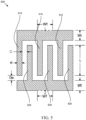
- capacitor 140 and/or 142 may be coupled to or integrally formed as a part of the substrate 101.
- the capacitor 140 may be directly coupled between conductive pads (e.g., between pads 261/262, 361/362, FIGs 2 , 3 ) of the substrate 101 to which the input terminals 121, 122 are connected.
- capacitor 142 may be directly coupled between conductive pads (e.g., between pads 263/264, 363/364, FIGs 2 , 3 ) of the substrate 101 to which the output terminals 123, 124 are connected. For example, as shown in FIG.
- each amplifier 200, 300, 400 includes, at least, a printed circuit board (PCB) 201, 301, and 401 (or other suitable substrate) and a packaged semiconductor device 220, 320, 420.
- each power amplifier 200, 300, 400 may include input and output terminals (e.g., terminals 102, 104, FIG. 1 ), a power splitter (e.g., power splitter 110, FIG. 1 ), an output impedance inverter and phase shifter (e.g., component 180, FIG. 1 ), a combining node (e.g., combining node 170, FIG. 1 ), and an output transformer (e.g., transformer 190, FIG. 1 ).
- PCB printed circuit board
- a capacitor having a value of approximately 0.9 pF (e.g., 0.9 pF plus-or-minus X%, where X may be equal to one, two, three, .... ten) between a first transistor (e.g., carrier transistor 136, FIG. 1 ) and a second transistor (e.g., peaking transistor 156, FIG. 1 ) serves sufficiently well for reducing the impact of coupling between leads/wires (e.g., between bondwires 433, 453 or bondwires 446, 447, FIG.
- first transistor e.g., carrier transistor 136, FIG. 1
- a second transistor e.g., peaking transistor 156, FIG. 1
- aspects of this disclosure may readily lend themselves to conventional circuit, device, and PCB manufacturing/fabrication techniques.
- aspects of this disclosure may be implemented with little-to-no additional cost (in terms of, e.g., package development or innovation) or energy consumption/power dissipation relative to conventional techniques, while at the same time providing additional benefits in terms of achieving/realizing isolation.
- aspects of this disclosure represent substantial improvements relative to conventional technologies in terms of practical applications involving circuit design and assembly/fabrication/manufacture.
- the various aspects of this disclosure are not directed to abstract ideas. To the contrary, the various aspects of this disclosure are directed to, and encompass, significantly more than any abstract idea standing alone.
Landscapes
- Engineering & Computer Science (AREA)
- Power Engineering (AREA)
- Microelectronics & Electronic Packaging (AREA)
- Amplifiers (AREA)
Priority Applications (3)
| Application Number | Priority Date | Filing Date | Title |
|---|---|---|---|
| EP23307397.2A EP4579743A1 (fr) | 2023-12-27 | 2023-12-27 | Amplificateur de puissance à trajets multiples avec condensateur pour compenser un couplage entre des trajets d'amplificateur |
| CN202411777595.1A CN120222975A (zh) | 2023-12-27 | 2024-12-05 | 具有用于补偿放大器路径间的耦合的电容器的功率放大器 |
| US18/971,078 US20250219587A1 (en) | 2023-12-27 | 2024-12-06 | Multiple-path power amplifier with capacitor for compensating for a coupling between amplifier paths |
Applications Claiming Priority (1)
| Application Number | Priority Date | Filing Date | Title |
|---|---|---|---|
| EP23307397.2A EP4579743A1 (fr) | 2023-12-27 | 2023-12-27 | Amplificateur de puissance à trajets multiples avec condensateur pour compenser un couplage entre des trajets d'amplificateur |
Publications (1)
| Publication Number | Publication Date |
|---|---|
| EP4579743A1 true EP4579743A1 (fr) | 2025-07-02 |
Family
ID=89619848
Family Applications (1)
| Application Number | Title | Priority Date | Filing Date |
|---|---|---|---|
| EP23307397.2A Pending EP4579743A1 (fr) | 2023-12-27 | 2023-12-27 | Amplificateur de puissance à trajets multiples avec condensateur pour compenser un couplage entre des trajets d'amplificateur |
Country Status (3)
| Country | Link |
|---|---|
| US (1) | US20250219587A1 (fr) |
| EP (1) | EP4579743A1 (fr) |
| CN (1) | CN120222975A (fr) |
Citations (2)
| Publication number | Priority date | Publication date | Assignee | Title |
|---|---|---|---|---|
| US20080224771A1 (en) * | 2005-07-05 | 2008-09-18 | Freescale Semiconductor, Inc. | Compensation for Parasitic Coupling Between Rf or Microwave Transistors in the Same Package |
| US10862434B1 (en) * | 2019-10-29 | 2020-12-08 | Nxp Usa, Inc. | Asymmetric Doherty amplifier with complex combining load matching circuit |
-
2023
- 2023-12-27 EP EP23307397.2A patent/EP4579743A1/fr active Pending
-
2024
- 2024-12-05 CN CN202411777595.1A patent/CN120222975A/zh active Pending
- 2024-12-06 US US18/971,078 patent/US20250219587A1/en active Pending
Patent Citations (2)
| Publication number | Priority date | Publication date | Assignee | Title |
|---|---|---|---|---|
| US20080224771A1 (en) * | 2005-07-05 | 2008-09-18 | Freescale Semiconductor, Inc. | Compensation for Parasitic Coupling Between Rf or Microwave Transistors in the Same Package |
| US10862434B1 (en) * | 2019-10-29 | 2020-12-08 | Nxp Usa, Inc. | Asymmetric Doherty amplifier with complex combining load matching circuit |
Also Published As
| Publication number | Publication date |
|---|---|
| CN120222975A (zh) | 2025-06-27 |
| US20250219587A1 (en) | 2025-07-03 |
Similar Documents
| Publication | Publication Date | Title |
|---|---|---|
| US10594266B2 (en) | Multiple-path amplifier with series component along inverter between amplifier outputs | |
| EP3799303B1 (fr) | Module d'amplificateur de doherty compact à trois voies | |
| EP3496269A1 (fr) | Amplificateurs de puissance à large bande ayant des pièges harmoniques | |
| EP2458730A1 (fr) | Amplificateur radiofréquence | |
| EP3782281B1 (fr) | Amplificateur de puissance radiofréquence comprenant un circuit de commande d'harmonique, et son procédé de fabrication | |
| US7206551B2 (en) | High frequency switch module and multi-layer substrate for high frequency switch module | |
| EP3849078B1 (fr) | Amplificateurs de puissance à plusieurs étages et dispositifs avec étages de commande basse tension | |
| US11522497B2 (en) | Doherty amplifier incorporating output matching network with integrated passive devices | |
| US11705870B2 (en) | Integrally-formed splitter for multiple-path power amplifiers and methods of manufacture thereof | |
| CN109194295B (zh) | 一种介质集成悬置线wlan双通带低噪声放大器 | |
| US20210391829A1 (en) | Symmetric doherty amplifier with in-package combining node | |
| CN117546407A (zh) | 结合内部连接的输出集成晶体管放大器器件封装 | |
| US20230079916A1 (en) | T-match topology with baseband termination | |
| US12537483B2 (en) | Amplifier device with low frequency resonance decoupling circuitry | |
| US12199571B2 (en) | Hybrid Doherty power amplifier module | |
| US11677367B2 (en) | Power amplifier circuit | |
| EP4372984B1 (fr) | Dispositifs amplificateurs de puissance avec circuits d'adaptation en boîtier qui fournissent une opération de classe f pseudo-inverse | |
| US20250219587A1 (en) | Multiple-path power amplifier with capacitor for compensating for a coupling between amplifier paths | |
| CN115567004A (zh) | 一种三路Doherty射频功率放大器 | |
| CN219164528U (zh) | 一种带外信号抑制电路及印刷电路板 | |
| JP2013115760A (ja) | ドハティ増幅器 | |
| EP4651372A1 (fr) | Amplificateur de puissance doherty à transformateur d'impédance de sortie reconfigurable | |
| EP4742529A1 (fr) | Amplificateur de puissance double avec circuit combinateur de sortie accordable | |
| US12537485B2 (en) | Power amplifier | |
| US20260135517A1 (en) | Dual power amplifier with tunable output combiner circuit |
Legal Events
| Date | Code | Title | Description |
|---|---|---|---|
| PUAI | Public reference made under article 153(3) epc to a published international application that has entered the european phase |
Free format text: ORIGINAL CODE: 0009012 |
|
| STAA | Information on the status of an ep patent application or granted ep patent |
Free format text: STATUS: THE APPLICATION HAS BEEN PUBLISHED |
|
| AK | Designated contracting states |
Kind code of ref document: A1 Designated state(s): AL AT BE BG CH CY CZ DE DK EE ES FI FR GB GR HR HU IE IS IT LI LT LU LV MC ME MK MT NL NO PL PT RO RS SE SI SK SM TR |
|
| STAA | Information on the status of an ep patent application or granted ep patent |
Free format text: STATUS: REQUEST FOR EXAMINATION WAS MADE |
|
| 17P | Request for examination filed |
Effective date: 20260102 |