EP4579751A1 - Festkörper-bildaufnahmevorrichtung - Google Patents
Festkörper-bildaufnahmevorrichtung Download PDFInfo
- Publication number
- EP4579751A1 EP4579751A1 EP23857183.0A EP23857183A EP4579751A1 EP 4579751 A1 EP4579751 A1 EP 4579751A1 EP 23857183 A EP23857183 A EP 23857183A EP 4579751 A1 EP4579751 A1 EP 4579751A1
- Authority
- EP
- European Patent Office
- Prior art keywords
- capacitive element
- wiring
- state imaging
- solid
- mim
- Prior art date
- Legal status (The legal status is an assumption and is not a legal conclusion. Google has not performed a legal analysis and makes no representation as to the accuracy of the status listed.)
- Pending
Links
Images









Classifications
-
- H—ELECTRICITY
- H04—ELECTRIC COMMUNICATION TECHNIQUE
- H04N—PICTORIAL COMMUNICATION, e.g. TELEVISION
- H04N25/00—Circuitry of solid-state image sensors [SSIS]; Control thereof
- H04N25/70—SSIS architectures; Circuits associated therewith
- H04N25/76—Addressed sensors, e.g. MOS or CMOS sensors
- H04N25/77—Pixel circuitry, e.g. memories, A/D converters, pixel amplifiers, shared circuits or shared components
- H04N25/771—Pixel circuitry, e.g. memories, A/D converters, pixel amplifiers, shared circuits or shared components comprising storage means other than floating diffusion
-
- H—ELECTRICITY
- H04—ELECTRIC COMMUNICATION TECHNIQUE
- H04N—PICTORIAL COMMUNICATION, e.g. TELEVISION
- H04N25/00—Circuitry of solid-state image sensors [SSIS]; Control thereof
- H04N25/50—Control of the SSIS exposure
- H04N25/57—Control of the dynamic range
- H04N25/59—Control of the dynamic range by controlling the amount of charge storable in the pixel, e.g. modification of the charge conversion ratio of the floating node capacitance
-
- H—ELECTRICITY
- H10—SEMICONDUCTOR DEVICES; ELECTRIC SOLID-STATE DEVICES NOT OTHERWISE PROVIDED FOR
- H10F—INORGANIC SEMICONDUCTOR DEVICES SENSITIVE TO INFRARED RADIATION, LIGHT, ELECTROMAGNETIC RADIATION OF SHORTER WAVELENGTH OR CORPUSCULAR RADIATION
- H10F39/00—Integrated devices, or assemblies of multiple devices, comprising at least one element covered by group H10F30/00, e.g. radiation detectors comprising photodiode arrays
- H10F39/10—Integrated devices
- H10F39/12—Image sensors
- H10F39/18—Complementary metal-oxide-semiconductor [CMOS] image sensors; Photodiode array image sensors
-
- H—ELECTRICITY
- H10—SEMICONDUCTOR DEVICES; ELECTRIC SOLID-STATE DEVICES NOT OTHERWISE PROVIDED FOR
- H10F—INORGANIC SEMICONDUCTOR DEVICES SENSITIVE TO INFRARED RADIATION, LIGHT, ELECTROMAGNETIC RADIATION OF SHORTER WAVELENGTH OR CORPUSCULAR RADIATION
- H10F39/00—Integrated devices, or assemblies of multiple devices, comprising at least one element covered by group H10F30/00, e.g. radiation detectors comprising photodiode arrays
- H10F39/80—Constructional details of image sensors
- H10F39/803—Pixels having integrated switching, control, storage or amplification elements
-
- H—ELECTRICITY
- H10—SEMICONDUCTOR DEVICES; ELECTRIC SOLID-STATE DEVICES NOT OTHERWISE PROVIDED FOR
- H10F—INORGANIC SEMICONDUCTOR DEVICES SENSITIVE TO INFRARED RADIATION, LIGHT, ELECTROMAGNETIC RADIATION OF SHORTER WAVELENGTH OR CORPUSCULAR RADIATION
- H10F39/00—Integrated devices, or assemblies of multiple devices, comprising at least one element covered by group H10F30/00, e.g. radiation detectors comprising photodiode arrays
- H10F39/80—Constructional details of image sensors
- H10F39/803—Pixels having integrated switching, control, storage or amplification elements
- H10F39/8037—Pixels having integrated switching, control, storage or amplification elements the integrated elements comprising a transistor
-
- H—ELECTRICITY
- H10—SEMICONDUCTOR DEVICES; ELECTRIC SOLID-STATE DEVICES NOT OTHERWISE PROVIDED FOR
- H10F—INORGANIC SEMICONDUCTOR DEVICES SENSITIVE TO INFRARED RADIATION, LIGHT, ELECTROMAGNETIC RADIATION OF SHORTER WAVELENGTH OR CORPUSCULAR RADIATION
- H10F39/00—Integrated devices, or assemblies of multiple devices, comprising at least one element covered by group H10F30/00, e.g. radiation detectors comprising photodiode arrays
- H10F39/80—Constructional details of image sensors
- H10F39/809—Constructional details of image sensors of hybrid image sensors
-
- H—ELECTRICITY
- H10—SEMICONDUCTOR DEVICES; ELECTRIC SOLID-STATE DEVICES NOT OTHERWISE PROVIDED FOR
- H10F—INORGANIC SEMICONDUCTOR DEVICES SENSITIVE TO INFRARED RADIATION, LIGHT, ELECTROMAGNETIC RADIATION OF SHORTER WAVELENGTH OR CORPUSCULAR RADIATION
- H10F39/00—Integrated devices, or assemblies of multiple devices, comprising at least one element covered by group H10F30/00, e.g. radiation detectors comprising photodiode arrays
- H10F39/80—Constructional details of image sensors
- H10F39/811—Interconnections
-
- H—ELECTRICITY
- H10—SEMICONDUCTOR DEVICES; ELECTRIC SOLID-STATE DEVICES NOT OTHERWISE PROVIDED FOR
- H10F—INORGANIC SEMICONDUCTOR DEVICES SENSITIVE TO INFRARED RADIATION, LIGHT, ELECTROMAGNETIC RADIATION OF SHORTER WAVELENGTH OR CORPUSCULAR RADIATION
- H10F39/00—Integrated devices, or assemblies of multiple devices, comprising at least one element covered by group H10F30/00, e.g. radiation detectors comprising photodiode arrays
- H10F39/10—Integrated devices
- H10F39/12—Image sensors
- H10F39/199—Back-illuminated image sensors
Definitions
- a structure of a pixel of an image sensor there is known a structure that is provided with a storage capacitance that stores charges having overflown from a photodiode (see, for example, PTL 1 and PTL 2).
- the storage capacitances are disposed as a two-stage structure in the structure disclosed in PTL 2 to achieve a wider dynamic range while keeping the SN ratio, two storage capacitances are disposed on the same plane as that of the photodiode, and therefore an area of a plane on a light incidence surface side of the photodiode is limited. Hence, a technique for achieving desired characteristics with a more appropriate layout is demanded.
- a solid-state imaging device includes: a plurality of pixels that each include a photoelectric conversion element and a plurality of wiring capacitive elements; and a read-out unit that reads out signals from the plurality of pixels, the solid-state imaging device has a structure that a charge having overflown from the photoelectric conversion element is stored in a first wiring capacitive element, and the charge having overflown from the first wiring capacitive element is stored in a second wiring capacitive element, and the read-out unit individually reads out a signal of each of the photoelectric conversion element, the first wiring capacitive element, and the second wiring capacitive element.
- the solid-state imaging device has the structure that the charge having overflown from the photoelectric conversion element is stored in the first wiring capacitive element, and the charge having overflown from the first wiring capacitive element is stored in the second wiring capacitive element, and individually reads out the signal of each of the photoelectric conversion element, the first wiring capacitive element, and the second wiring capacitive element.
- a solid-state imaging device includes: a plurality of pixels that each include a plurality of photoelectric conversion elements and a plurality of wiring capacitive elements; and a read-out unit that reads out signals from the plurality of pixels, the solid-state imaging device has a structure that a first wiring capacitive element and a second wiring capacitive element are respectively connected to floating diffusions of a first photoelectric conversion element and a second photoelectric conversion element, and a charge having overflown from the first photoelectric conversion element is stored in the first wiring capacitive element, and the charge having overflown from the second photoelectric conversion element is stored in the second wiring capacitive element, and the read-out unit individually reads out a signal of each of the first photoelectric conversion element, the second photoelectric conversion element, the first wiring capacitive element, and the second wiring capacitive element.
- the solid-state imaging device has the structure that the charge having overflown from the first photoelectric conversion element is stored in the first wiring capacitive element, and the charge having overflown from the second photoelectric conversion element is stored in the second wiring capacitive element, and individually reads out the signal of each of the first photoelectric conversion element, the second photoelectric conversion element, the first wiring capacitive element, and the second wiring capacitive element.
- solid-state imaging device may be an independent device or may be an internal block constituting one device.
- Fig. 1 is a diagram illustrating a configuration example of one embodiment of a solid-state imaging device to which the present disclosure is applied.
- a solid-state imaging device 10 is a Complementary Metal Oxide Semiconductor (CMOS) type solid-state imaging device.
- the solid-state imaging device 10 includes a pixel array unit 21, a vertical drive unit 22, a column signal processing unit 23, a horizontal drive unit 24, an output unit 25, and a control unit 26.
- CMOS Complementary Metal Oxide Semiconductor
- the pixel array unit 21 includes a plurality of pixels 100 two-dimensionally aligned in a matrix on a semiconductor substrate made of silicon (Si) or the like.
- the pixel 100 includes a photodiode, a plurality of pixel transistors, and the like.
- a pixel drive line 41 is formed per row and connected to the vertical drive unit 22, and a vertical signal line 42 is formed per column and is connected to the column signal processing unit 23 for the plurality of pixels 100 two-dimensionally aligned in the matrix.
- the solid-state imaging device 10 has the multistage structure (two-stage structure) that the MIM capacitive element 131 and the MIM capacitive element 132 having the different capacitances are disposed per pixel 100, and charges having overflown from the photodiode 111 are stored in the MIM capacitive element 131 and the MIM capacitive element 132, and signals obtained from the charges stored in the photodiode 111, the MIM capacitive element 131, and the MIM capacitive element 132 are individually read out.
- the MIM capacitive element 131 and the MIM capacitive element 132 are wiring capacitive elements, and are disposed between wiring layers, so that the MIM capacitive element 131 and the MIM capacitive element 132 are not disposed on the same plane as that of the photodiode 111, and do not limit the area of the photodiode 111 (the area of the plane on the light incidence surface side). Furthermore, the photodiode 111, the MIM capacitive element 131, and the MIM capacitive element 132 are not disposed on the same plane, so that there is also an advantage for miniaturization of pixels.
- the pixel 100 has the first structure ( Fig. 2 and the other figures), so that the photodiode 111 and the MIM capacitive elements 131 and 132 are not disposed on the same plane, and it is possible to achieve both of suppression of deterioration of the SN ratio and expansion of the dynamic range. That is, it is possible to achieve desired characteristics with a more appropriate layout.
- Fig. 9 is a cross-sectional view illustrating a second example of a structure of a pixel.
- the MIM capacitive element 131 and the MIM capacitive element 132 are disposed at the same position in the Z direction, and are disposed between the same wiring layers. That is, in the wiring layer 12, both of the MIM capacitive element 131 and the MIM capacitive element 132 are disposed between the first wiring layers.
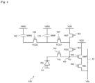
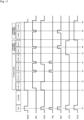
- Fig. 12 is a timing chart for describing an example of a read-out operation of the circuit configuration in Fig. 11 .
- the common control signal VMID for the MIM capacitive elements 131 and 132 are changed to the control signal VMID1 for the MIM capacitive element 131, and the control signal VMID2 for the MIM capacitive element 132. Consequently, the MIM capacitive element 131 and the MIM capacitive element 132 are individually controlled. Since a timing of a drive signal such as SEL in Fig. 12 is similar to that in Fig. 6 , description thereof will be omitted.
- FIG. 11 illustrates the example of the TG type circuit configuration
- the OFG type circuit configuration can also adopt the same configuration.
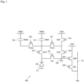
- Fig. 13 is a diagram illustrating another example of the OFG type circuit configuration illustrated in Fig. 7 .
- the upper electrode of the MIM capacitive element 131 is connected to the control power supply VMID 1
- the upper electrode of the MIM capacitive element 132 is connected to the control power supply VMID2, so that it is possible to individually control the MIM capacitive element 131 and the MIM capacitive element 132.
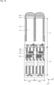
- Light incidence surface sides of the photodiode 211-1 and the photodiode 211-2 are provided with a color filter 201 and an on-chip microlens 202. As illustrated in the plan view of Fig. 15 , three on-chip microlenses 202-1-1 to 202-1-3 are provided to meet the L-shaped region of the photodiode 211-1, and one on-chip microlens 202-2 is provided to meet the rectangular region of the photodiode 211-2.
- the wiring layer 12 is a multilayer wiring layer that includes a plurality of wiring layers obtained by being stacked at a plurality of stages and forming a wiring 222 in each stage with an inter-wiring film 221 interposed therebetween.
- an MIM capacitive element 231 and an MIM capacitive element 232 are disposed as wiring capacitive elements having different capacitances.
- the MIM capacitive element 231 and the MIM capacitive element 232 are provided per pixel 100.
- the MIM capacitive element 231 and the MIM capacitive element 232 are disposed between different wiring layers.
- the MIM capacitive element 231 and the MIM capacitive element 232 can have the three-dimensional structures similar to the structure illustrated in Fig. 3 .
- the MIM capacitive element 231 and the MIM capacitive element 232 can have the structures whose at least ones of the film types, the thicknesses, and the areas of the dielectrics are different.
- the capacitance of the MIM capacitive element 232 is larger than the capacitance of the MIM capacitive element 231.
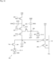
- Fig. 16 is a diagram illustrating an example of the circuit configuration of the pixel 100 in Fig. 14 .
- the pixel 100 includes the photodiodes 211-1 and 211-2, the MIM capacitive elements 231 and 232, a transfer transistor 261, an FD 262, a switch transistor 263, a reset transistor 264, an amplifier transistor 265, a selection transistor 266, a switch transistor 267, a storage transistor 268, and an FD 269.
- the transfer transistor 261 is provided between the photodiode 211-1 and the FD 262, and transfers the charge stored in the photodiode 211-1 to the FD 262 according to the drive signal TGL to be applied to a gate voltage of the transfer transistor 261.
- the FD 262 is a floating diffusion that converts the charge from the photodiode 211-1 into a voltage signal.
- the FD 262 is connected with the vertical signal line 42 via the amplifier transistor 265 and the selection transistor 266.
- the switch transistor 263 switches a connection state between the FD 262, the switch transistor 267, and the storage transistor 268 according to the drive signal FDG to be applied to a gate voltage of the switch transistor 263.
- the switch transistor 267 switches a connection state between the switch transistor 263, the MIM capacitive element 231, and the reset transistor 264 according to the drive signal LCG to be applied to a gate voltage of the switch transistor 267.
- the storage transistor 268 switches a connection state between the switch transistor 263 and the FD 269 according to the drive signal FCG to be applied to a gate electrode of the storage transistor 268.
- VMID represents a common control signal of the MIM capacitive elements 231 and 232 in the circuit diagram in Fig. 16 .
- SEL, FDG, TGL, RST, LCG, and FCG represent drive signals to be applied to the gate electrode of each transistor in the circuit diagram in Fig. 16 .
- the cross-sectional view of Fig. 14 illustrates the case where the MIM capacitive element 231 and the MIM capacitive element 232 are disposed between the different wiring layers
- the MIM capacitive element 231 and the MIM capacitive element 232 may be disposed between the same wiring layers.
- the inter-pixel isolation part 212 is formed as the trench formed penetrating the surface on the side opposite to the light incidence surface in the cross-sectional view of Fig. 14
- the solid-state imaging device 10 has been described as a CMOS type solid-state imaging device in the above description, and the CMOS type solid-state imaging device can have a back-illuminated structure in which light is incident from the upper layer (back surface side) located on the side opposite to the wiring layer side (front surface side) formed in the lower layer when viewed from the semiconductor substrate in which the photodiode 111 is formed as the photoelectric conversion unit.
- the CMOS type solid-state imaging device may have a front-illuminated structure in which the side on which light is incident is the wiring layer side (front surface side).
- the solid-state imaging device 10 is an example of the light detection device to which the present disclosure is applied. That is, the light detection device to which the present disclosure is applied is not limited to the solid-state imaging device 10, and is applicable to, for example, a device that detects light such as a distance measurement sensor that uses an IR laser. Note that the configuration to which the present disclosure is applied is not limited to the CMOS type solid-state imaging device, and is also applicable to other solid-state imaging devices such as the Charge Coupled Device (CCD) type.
- CCD Charge Coupled Device
- the solid-state imaging device to which the present disclosure is applied can be installed in an electronic device such as a smartphone, a tablet terminal, a mobile phone, a digital still camera, and a digital video camera.
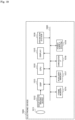
- Fig. 19 is a block diagram illustrating a configuration example of an electronic device including the built-in solid-state imaging device to which the present disclosure is applied.
- the CPU 1010 controls an operation of each unit of the electronic device 1000.
- the optical system 1011 captures incident light (image light) from a subject and forms an image on a light detection surface of the solid-state imaging device 1012.
- the solid-state imaging device 1012 converts the light amount of incident light, with which an image is formed on the light detection surface by the optical system 1011, into an electrical signal in units of pixels, and outputs the electrical signal as a signal.
- the DSP 1013 performs predetermined signal processing on the signal output from the solid-state imaging device 1012.
- the frame memory 1014 temporarily records image data of a still image or a video captured by the imaging system.
- the display 1015 is a liquid crystal display or an organic EL display, and displays a still image or a video captured by the imaging system.
- the operation system 1016 issues an operation command for various functions of the electronic device 1000 in response to a user operation.
Landscapes
- Engineering & Computer Science (AREA)
- Multimedia (AREA)
- Signal Processing (AREA)
- Solid State Image Pick-Up Elements (AREA)
- Transforming Light Signals Into Electric Signals (AREA)
Applications Claiming Priority (2)
| Application Number | Priority Date | Filing Date | Title |
|---|---|---|---|
| JP2022131496 | 2022-08-22 | ||
| PCT/JP2023/028856 WO2024043069A1 (ja) | 2022-08-22 | 2023-08-08 | 固体撮像装置 |
Publications (2)
| Publication Number | Publication Date |
|---|---|
| EP4579751A1 true EP4579751A1 (de) | 2025-07-02 |
| EP4579751A4 EP4579751A4 (de) | 2025-12-03 |
Family
ID=90013088
Family Applications (1)
| Application Number | Title | Priority Date | Filing Date |
|---|---|---|---|
| EP23857183.0A Pending EP4579751A4 (de) | 2022-08-22 | 2023-08-08 | Festkörper-bildaufnahmevorrichtung |
Country Status (6)
| Country | Link |
|---|---|
| US (1) | US20260032360A1 (de) |
| EP (1) | EP4579751A4 (de) |
| JP (1) | JPWO2024043069A1 (de) |
| CN (1) | CN119563395A (de) |
| TW (1) | TW202425302A (de) |
| WO (1) | WO2024043069A1 (de) |
Families Citing this family (2)
| Publication number | Priority date | Publication date | Assignee | Title |
|---|---|---|---|---|
| TW202549593A (zh) * | 2024-03-19 | 2025-12-16 | 日商索尼半導體解決方案公司 | 光檢測元件及電子機器 |
| WO2026018662A1 (ja) * | 2024-07-19 | 2026-01-22 | ソニーセミコンダクタソリューションズ株式会社 | 容量素子、撮像素子 |
Family Cites Families (15)
| Publication number | Priority date | Publication date | Assignee | Title |
|---|---|---|---|---|
| US6888122B2 (en) * | 2002-08-29 | 2005-05-03 | Micron Technology, Inc. | High dynamic range cascaded integration pixel cell and method of operation |
| JP5066704B2 (ja) * | 2005-02-04 | 2012-11-07 | 国立大学法人東北大学 | 固体撮像装置、および固体撮像装置の動作方法 |
| US7821560B2 (en) * | 2005-04-07 | 2010-10-26 | Tohoku Universityu | Optical sensor, solid-state imaging device, and operating method of solid-state imaging device |
| JP6719984B2 (ja) * | 2016-06-06 | 2020-07-08 | キヤノン株式会社 | 撮像装置、撮像システム |
| WO2018190363A1 (ja) * | 2017-04-12 | 2018-10-18 | ブリルニクスジャパン株式会社 | 固体撮像装置、固体撮像装置の駆動方法、および電子機器 |
| US10847316B2 (en) * | 2018-09-20 | 2020-11-24 | Taiwan Semiconductor Manufacturing Co., Ltd. | MIM device with laminated dielectric layers |
| KR102661820B1 (ko) * | 2019-02-11 | 2024-05-02 | 삼성전자주식회사 | 이미지 센서 및 그것의 구동 방법 |
| CN113906732B (zh) * | 2019-05-31 | 2024-08-16 | 新唐科技日本株式会社 | 固体摄像装置及使用该固体摄像装置的摄像装置 |
| KR102771906B1 (ko) * | 2019-11-06 | 2025-02-28 | 삼성전자주식회사 | 이미지 센서 및 그 제조 방법 |
| CN115066887B (zh) * | 2020-02-18 | 2025-10-21 | 新唐科技日本株式会社 | 固体摄像装置以及利用固体摄像装置的摄像装置 |
| US20230307473A1 (en) * | 2020-07-17 | 2023-09-28 | Sony Semiconductor Solutions Corporation | Light receiving element, manufacturing method for same, and electronic device |
| JP7064537B2 (ja) * | 2020-07-29 | 2022-05-10 | ソニーセミコンダクタソリューションズ株式会社 | 固体撮像装置及びこれの制御方法 |
| US20230299113A1 (en) * | 2020-08-19 | 2023-09-21 | Sony Semiconductor Solutions Corporation | Solid-state imaging device and electronic device |
| CN116419082A (zh) * | 2021-12-31 | 2023-07-11 | 格科微电子(上海)有限公司 | 高动态成像的实现方法及其装置、图像处理系统 |
| KR20240037026A (ko) * | 2022-09-14 | 2024-03-21 | 삼성전자주식회사 | 이미지 센서 |
-
2023
- 2023-07-05 TW TW112125037A patent/TW202425302A/zh unknown
- 2023-08-08 CN CN202380052361.8A patent/CN119563395A/zh active Pending
- 2023-08-08 EP EP23857183.0A patent/EP4579751A4/de active Pending
- 2023-08-08 JP JP2024542729A patent/JPWO2024043069A1/ja active Pending
- 2023-08-08 WO PCT/JP2023/028856 patent/WO2024043069A1/ja not_active Ceased
- 2023-08-08 US US18/997,324 patent/US20260032360A1/en active Pending
Also Published As
| Publication number | Publication date |
|---|---|
| WO2024043069A1 (ja) | 2024-02-29 |
| EP4579751A4 (de) | 2025-12-03 |
| US20260032360A1 (en) | 2026-01-29 |
| JPWO2024043069A1 (de) | 2024-02-29 |
| TW202425302A (zh) | 2024-06-16 |
| CN119563395A (zh) | 2025-03-04 |
Similar Documents
| Publication | Publication Date | Title |
|---|---|---|
| US11665452B2 (en) | Image sensor | |
| EP2758937B1 (de) | Abbildungssysteme mit gestapelten chips | |
| CN209845132U (zh) | 固态高动态范围图像传感器的像素电路和所述图像传感器 | |
| EP2230690B1 (de) | Bildaufnahmesensor, Herstellungsverfahren dazu, Verfahren zur Steuerung und elektronische Vorrichtung | |
| US7008816B2 (en) | Imager photo diode capacitor structure with reduced process variation sensitivity | |
| US10777601B1 (en) | CMOS image sensor with compact pixel layout | |
| CN108200367A (zh) | 像素单元和形成像素单元的方法及数字相机成像系统组件 | |
| JP7356214B2 (ja) | 撮像装置、その製造方法及びカメラ | |
| CN108282625A (zh) | 像素单元和形成像素单元的方法及数字相机成像系统组件 | |
| EP4579751A1 (de) | Festkörper-bildaufnahmevorrichtung | |
| CN108305884A (zh) | 像素单元和形成像素单元的方法及数字相机成像系统组件 | |
| US12610646B2 (en) | Image sensor | |
| US20150123173A1 (en) | 3d stacked image sensor with pmos components | |
| KR20220152457A (ko) | 이미지 센서 및 그 동작 방법 | |
| JP2008227357A (ja) | 固体撮像装置及びその製造方法 | |
| CN116525635A (zh) | Cmos图像传感器及其形成方法、车载摄像头 | |
| US12356741B2 (en) | Split floating diffusion pixel layout design | |
| US20250212546A1 (en) | Image sensor including stacked capacitors | |
| US12047694B2 (en) | Split floating diffusion pixel layout design | |
| US20250160030A1 (en) | Image sensor | |
| JP2025005675A (ja) | 固体撮像装置及び電子機器 | |
| CN121078818A (zh) | 成像装置 | |
| KR20070050593A (ko) | 이미지 센서 및 그 제조방법 |
Legal Events
| Date | Code | Title | Description |
|---|---|---|---|
| STAA | Information on the status of an ep patent application or granted ep patent |
Free format text: STATUS: THE INTERNATIONAL PUBLICATION HAS BEEN MADE |
|
| PUAI | Public reference made under article 153(3) epc to a published international application that has entered the european phase |
Free format text: ORIGINAL CODE: 0009012 |
|
| STAA | Information on the status of an ep patent application or granted ep patent |
Free format text: STATUS: REQUEST FOR EXAMINATION WAS MADE |
|
| 17P | Request for examination filed |
Effective date: 20250109 |
|
| AK | Designated contracting states |
Kind code of ref document: A1 Designated state(s): AL AT BE BG CH CY CZ DE DK EE ES FI FR GB GR HR HU IE IS IT LI LT LU LV MC ME MK MT NL NO PL PT RO RS SE SI SK SM TR |
|
| REG | Reference to a national code |
Ref country code: DE Ref legal event code: R079 Free format text: PREVIOUS MAIN CLASS: H01L0027146000 Ipc: H10F0039000000 |
|
| DAV | Request for validation of the european patent (deleted) | ||
| DAX | Request for extension of the european patent (deleted) | ||
| A4 | Supplementary search report drawn up and despatched |
Effective date: 20251103 |
|
| RIC1 | Information provided on ipc code assigned before grant |
Ipc: H10F 39/00 20250101AFI20251028BHEP Ipc: H04N 25/59 20230101ALI20251028BHEP Ipc: H04N 25/771 20230101ALI20251028BHEP Ipc: H10F 39/12 20250101ALI20251028BHEP Ipc: H10F 39/18 20250101ALI20251028BHEP |