EP4579762A1 - Solarzelle und fotovoltaisches modul - Google Patents
Solarzelle und fotovoltaisches modul Download PDFInfo
- Publication number
- EP4579762A1 EP4579762A1 EP24162248.9A EP24162248A EP4579762A1 EP 4579762 A1 EP4579762 A1 EP 4579762A1 EP 24162248 A EP24162248 A EP 24162248A EP 4579762 A1 EP4579762 A1 EP 4579762A1
- Authority
- EP
- European Patent Office
- Prior art keywords
- regions
- doped
- solar cell
- substrate
- dopant atoms
- Prior art date
- Legal status (The legal status is an assumption and is not a legal conclusion. Google has not performed a legal analysis and makes no representation as to the accuracy of the status listed.)
- Pending
Links
Images


Classifications
-
- H—ELECTRICITY
- H10—SEMICONDUCTOR DEVICES; ELECTRIC SOLID-STATE DEVICES NOT OTHERWISE PROVIDED FOR
- H10F—INORGANIC SEMICONDUCTOR DEVICES SENSITIVE TO INFRARED RADIATION, LIGHT, ELECTROMAGNETIC RADIATION OF SHORTER WAVELENGTH OR CORPUSCULAR RADIATION
- H10F10/00—Individual photovoltaic cells, e.g. solar cells
- H10F10/10—Individual photovoltaic cells, e.g. solar cells having potential barriers
- H10F10/16—Photovoltaic cells having only PN heterojunction potential barriers
-
- H—ELECTRICITY
- H10—SEMICONDUCTOR DEVICES; ELECTRIC SOLID-STATE DEVICES NOT OTHERWISE PROVIDED FOR
- H10F—INORGANIC SEMICONDUCTOR DEVICES SENSITIVE TO INFRARED RADIATION, LIGHT, ELECTROMAGNETIC RADIATION OF SHORTER WAVELENGTH OR CORPUSCULAR RADIATION
- H10F77/00—Constructional details of devices covered by this subclass
- H10F77/10—Semiconductor bodies
- H10F77/12—Active materials
-
- H—ELECTRICITY
- H10—SEMICONDUCTOR DEVICES; ELECTRIC SOLID-STATE DEVICES NOT OTHERWISE PROVIDED FOR
- H10F—INORGANIC SEMICONDUCTOR DEVICES SENSITIVE TO INFRARED RADIATION, LIGHT, ELECTROMAGNETIC RADIATION OF SHORTER WAVELENGTH OR CORPUSCULAR RADIATION
- H10F10/00—Individual photovoltaic cells, e.g. solar cells
- H10F10/10—Individual photovoltaic cells, e.g. solar cells having potential barriers
- H10F10/14—Photovoltaic cells having only PN homojunction potential barriers
- H10F10/146—Back-junction photovoltaic cells, e.g. having interdigitated base-emitter regions on the back side
-
- H—ELECTRICITY
- H10—SEMICONDUCTOR DEVICES; ELECTRIC SOLID-STATE DEVICES NOT OTHERWISE PROVIDED FOR
- H10F—INORGANIC SEMICONDUCTOR DEVICES SENSITIVE TO INFRARED RADIATION, LIGHT, ELECTROMAGNETIC RADIATION OF SHORTER WAVELENGTH OR CORPUSCULAR RADIATION
- H10F10/00—Individual photovoltaic cells, e.g. solar cells
- H10F10/10—Individual photovoltaic cells, e.g. solar cells having potential barriers
- H10F10/16—Photovoltaic cells having only PN heterojunction potential barriers
- H10F10/164—Photovoltaic cells having only PN heterojunction potential barriers comprising heterojunctions with Group IV materials, e.g. ITO/Si or GaAs/SiGe photovoltaic cells
- H10F10/165—Photovoltaic cells having only PN heterojunction potential barriers comprising heterojunctions with Group IV materials, e.g. ITO/Si or GaAs/SiGe photovoltaic cells the heterojunctions being Group IV-IV heterojunctions, e.g. Si/Ge, SiGe/Si or Si/SiC photovoltaic cells
-
- H—ELECTRICITY
- H10—SEMICONDUCTOR DEVICES; ELECTRIC SOLID-STATE DEVICES NOT OTHERWISE PROVIDED FOR
- H10F—INORGANIC SEMICONDUCTOR DEVICES SENSITIVE TO INFRARED RADIATION, LIGHT, ELECTROMAGNETIC RADIATION OF SHORTER WAVELENGTH OR CORPUSCULAR RADIATION
- H10F19/00—Integrated devices, or assemblies of multiple devices, comprising at least one photovoltaic cell covered by group H10F10/00, e.g. photovoltaic modules
- H10F19/80—Encapsulations or containers for integrated devices, or assemblies of multiple devices, having photovoltaic cells
-
- H—ELECTRICITY
- H10—SEMICONDUCTOR DEVICES; ELECTRIC SOLID-STATE DEVICES NOT OTHERWISE PROVIDED FOR
- H10F—INORGANIC SEMICONDUCTOR DEVICES SENSITIVE TO INFRARED RADIATION, LIGHT, ELECTROMAGNETIC RADIATION OF SHORTER WAVELENGTH OR CORPUSCULAR RADIATION
- H10F19/00—Integrated devices, or assemblies of multiple devices, comprising at least one photovoltaic cell covered by group H10F10/00, e.g. photovoltaic modules
- H10F19/90—Structures for connecting between photovoltaic cells, e.g. interconnections or insulating spacers
- H10F19/902—Structures for connecting between photovoltaic cells, e.g. interconnections or insulating spacers for series or parallel connection of photovoltaic cells
- H10F19/908—Structures for connecting between photovoltaic cells, e.g. interconnections or insulating spacers for series or parallel connection of photovoltaic cells for back-contact photovoltaic cells
-
- H—ELECTRICITY
- H10—SEMICONDUCTOR DEVICES; ELECTRIC SOLID-STATE DEVICES NOT OTHERWISE PROVIDED FOR
- H10F—INORGANIC SEMICONDUCTOR DEVICES SENSITIVE TO INFRARED RADIATION, LIGHT, ELECTROMAGNETIC RADIATION OF SHORTER WAVELENGTH OR CORPUSCULAR RADIATION
- H10F77/00—Constructional details of devices covered by this subclass
- H10F77/20—Electrodes
- H10F77/206—Electrodes for devices having potential barriers
- H10F77/211—Electrodes for devices having potential barriers for photovoltaic cells
- H10F77/219—Arrangements for electrodes of back-contact photovoltaic cells
-
- H—ELECTRICITY
- H10—SEMICONDUCTOR DEVICES; ELECTRIC SOLID-STATE DEVICES NOT OTHERWISE PROVIDED FOR
- H10F—INORGANIC SEMICONDUCTOR DEVICES SENSITIVE TO INFRARED RADIATION, LIGHT, ELECTROMAGNETIC RADIATION OF SHORTER WAVELENGTH OR CORPUSCULAR RADIATION
- H10F77/00—Constructional details of devices covered by this subclass
- H10F77/30—Coatings
- H10F77/306—Coatings for devices having potential barriers
- H10F77/311—Coatings for devices having potential barriers for photovoltaic cells
Definitions
- Embodiments of the present disclosure relate to the field of solar cell technology, and in particular to a solar cell and a photovoltaic module.
- the fossil energy has the defects of air pollution and limited reserves, while the solar energy has the advantages of cleanliness, no pollution, abundant resources, and the like. Therefore, the solar energy is gradually becoming a core clean energy taking place of the fossil energy. Because solar cells have excellent photoelectric conversion efficiency, the solar cells are becoming the focus of development for clean energy utilization.
- Embodiments of the present disclosure provide a solar cell and a photovoltaic module, which is at least conducive to increase of the open-circuit voltage and to improvement of the photoelectric conversion efficiency of the solar cells.
- a solar cell including: a substrate having a front surface and a rear surface opposite to each other, a tunneling layer formed on the rear surface of the substrate, and a doped conductive layer formed on the tunneling layer.
- the tunneling layer includes first regions and second regions, the first regions interleave with the second regions in a first direction, and the first regions include first dopant atoms.
- the doped conductive layer includes first doped regions and second doped regions, each first doped region of the first doped regions is formed on a respective first region of the first regions, and each second doped region of the second doped regions is formed on a respective second region of the second regions.
- the first doped regions have a doping type different from a doping type of the second doped regions, the first doped regions include the first dopant atoms, and an atomic percentage of the first dopant atoms in the first doped regions is lower than an atomic percentage of the first dopant atoms in the first regions.
- a ratio of the atomic percentage of the first dopant atoms in the first regions to the atomic percentage of the first dopant atoms in the first doped regions ranges from 1 to 5.
- the atomic percentage of the first dopant atoms in the first regions ranges from 1% to 10%.
- the atomic percentage of the first dopant atoms in the first doped regions ranges from 0.2% to 5%.
- the first dopant atoms are N-type atoms.
- the atomic percentage of the first dopant atoms in the first doped regions reduces in gradient.
- one respective first region of the first regions includes a first portion contacting with the substrate, and an atomic percentage of the first dopant atoms in the first portion is higher than the atomic percentage of the first dopant atoms in the respective first region.
- the atomic percentage of the first dopant atoms in the first portion ranges from 2% to 20%.
- a ratio of a thickness of the first portion to a thickness of the respective first region ranges from 0.25 to 0.5.
- the thickness of the first portion ranges from 0.25 nm to 1 nm.
- one respective first region of the first regions includes a second portion contacting with a corresponding first doped region, and an atomic percentage of the first dopant atoms in the second portion is higher than the atomic percentage of the first dopant atoms in the respective first region.
- the atomic percentage of the first dopant atoms in the second portion ranges from 2% to 20%.
- Some embodiments of the present disclosure provide a photovoltaic module, including: at least one cell string formed by connecting a plurality of solar cells as illustrated above, at least one encapsulation layer configured to cover a surface of the at least one cell string, and at least one cover plate configured to cover a surface of the at least one encapsulation layer away from the at least one cell string.
- a part such as a layer, film, area, or substrate
- the part may be “directly” on another part or a third part may be present between the two parts.
- a part is “directly on” another part, it means that a third part is not present between the two parts.
- a part is “generally” formed on another part, it means the part is not formed on the entire surface (or front surface) of another part and is also not formed in part of the edge of the entire surface.
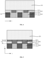
- the IBC cell may further include isolation layers 50 penetrating through the thickness of the doped conductive layer 30, and the isolation layers 50 are formed between the first doped regions 31 and the second doped regions 32 and configured to isolate the first doped regions 31 and the second doped regions 32 having different doping types from each other.
- the isolation layers 50 may be insulating dielectric layers formed by depositing an insulating dielectric, or may be a groove formed by patterned etching.
- FIG. 1 takes the isolation layers 50 only penetrating through the thickness of the doped conductive layer 30 as an example for description. In practice, the isolation layers 50 may further extend towards the interior of the tunneling dielectric layer 20 and even penetrate through the thickness of the tunneling dielectric layer 20, which is not specifically limited in the embodiments of the present disclosure.
- Some embodiments of the present disclosure provide a solar cell, a passivation contact structure formed by a tunneling layer and a doped conductive layer is disposed on a rear surface of a substrate of the solar cell, which can significantly reduce recombination of carriers occurred on the rear surface of the substrate, thereby reducing the recombination current on the rear surface of the substrate, and reducing the carrier recombination loss of the solar cell.
- the doped conductive layer is formed by first doped regions and second doped regions having different doping types, in this way, electrodes of the solar cell can be disposed on the rear surface of the solar cell, thereby significantly reducing the influence on the light absorption of the cell caused by disposing electrodes on the front surface of the solar cell, and improving the light absorption of the solar cell.
- the tunneling layer is formed by first regions and second regions, the first regions interleave with the second regions in a first direction, each first doped region of the first doped regions is formed on a respective first region of the first regions, each first region and each first doped region include first dopant atoms, and the atomic percentage of the first dopant atoms in the first regions is higher than the atomic percentage of the first dopant atoms in the first doped regions.
- the open-circuit voltage of the solar cell can be increased, and by doping the first dopant atoms in the tunneling layer, the tunneling ability of carriers in the tunneling layer can be improved, thereby significantly improving the photoelectric conversion efficiency of the solar cell.
- the first doped regions 131 have a doping type different from a doping type of the second doped regions 132.
- the first doped regions 131 include the first dopant atoms, and the atomic percentage of the first dopant atoms in the first doped regions 131 is lower than the atomic percentage of the first dopant atoms in the first regions 121.
- a passivation contact structure formed by the tunneling layer 102 and the doped conductive layer 103 is disposed on the rear surface of the substrate 101, the tunneling layer 102 passivates the defects on the surface of the substrate 101 by bonding, and the doped conductive layer 103 applies field passivation to the substrate 101 using a formed electric field, thereby significantly reducing the recombination of carriers occurred on the rear surface of the substrate 101, and reducing the carrier recombination loss of the solar cell.
- the plurality of isolation layers 50 may be grooves penetrating through the thickness of the stacked structure, or a plurality of dielectric layers formed by a non-conductive insulating dielectric material.
- the plurality of isolation layers 50 penetrating through the tunneling layer 102 and the doped conductive layer 103 are taken as an example for description.
- the plurality of isolation layers 50 may only penetrate through the thickness of the doped conductive layer 103, or penetrate through the thickness of the doped conductive layer 103 and extend towards the interior of the tunneling layer 102 by a certain distance, which are not specifically limited in the embodiments of the present disclosure.
- the material of the tunneling layer 102 may be at least one of silicon oxide, silicon nitride, silicon oxynitride, silicon carbide or magnesium fluoride.
- the material of the doped conductive layer 103 may be at least one of nanocrystalline silicon, polycrystalline silicon, microcrystalline silicon, amorphous silicon, silicon carbide or titanium nitride.
- a ratio of the atomic percentage of the first dopant atoms in the first regions 121 to the atomic percentage of the first dopant atoms in the first doped regions 131 ranges from 1 to 5.
- an N-type substrate 101, first regions 121 and first doped regions 131 of N doping type, and a doped element being phosphorus are taken as an example.
- the tunneling layer 102 and the doped conductive layer 103 have a main function of providing good passivation to the substrate 101, thereby reducing the carrier recombination occurred on the rear surface of the substrate 101, and increasing the open-circuit voltage and improving the photoelectric conversion efficiency of the solar cell.
- the enrichment of phosphorus in the first regions 121 of the tunneling layer 102 is achieved, and the passivation contact structure on the rear surface of the substrate 101 can provide a better passivation effect to the substrate 101, thereby further increasing the open-circuit voltage of the solar cell, and reducing the carrier recombination occurred on the rear surface of the substrate 101.
- the tunneling layer 102 has another function of achieving selective transfer of carriers.
- the doped conductive layer 103 is composed of the first doped regions 131 and the second doped regions 132 of different doping types
- the doped elements in the first regions 121 and the first doped region 131 are both phosphorus, and the first regions 121 needs to achieve selective transfer of holes to the first doped regions 131.
- the atomic percentage of the first dopant atoms in the second portions 324 is too high, during transfer of carriers to the first doped regions 331, the recombination of electrons and holes in the second portions 324 is too strong, which is prone to lead to a significant increase in overall carrier recombination loss in the first regions 321, and even lead to a significant increase in overall carrier recombination loss of the solar cell.
- the tunneling layer 302 includes a plurality of first regions 321, and the atomic percentages of the first dopant atoms in the second portions 324 of the plurality of first regions 321 may be the same or different from each other, which is not specifically limited in the embodiments of the present disclosure.
- a ratio of the thickness of a second portion 324 to the thickness of a corresponding first region 321 ranges from 0.25 to 0.5.
- the thickness of one respective second portion 324 refers to an average distance h3 between two surfaces of the respective second portion 324 opposite to each other in the direction perpendicular to the rear surface of the substrate 301
- the thickness of one respective first region 321 refers to an average distance h2 between two surfaces of the respective first region 321 opposite to each other in the direction perpendicular to the rear surface of the substrate 301.
- the second portions 324 are conducive to enhancing the passivation effect provided by the passivation contact structure to the substrate 301, and on the other hand, the recombination effect of electrons and holes in the second portions 324 is also significantly enhanced, which is prone to influence the overall carrier recombination loss of the first regions 321 and the solar cell.
- the carrier recombination loss occurred in the second portions 324 is determined, on the one hand, by the atomic percentage of the first dopant atoms in the second portions 324, and on the other hand, by the movement distances of carriers during transfer of carriers through the second portions 324.
- the atomic percentage of the first dopant atoms is fixed, the thicker the second portions 324 are, the larger the carrier recombination loss occurred in the second portions 324.
- the thickness of one respective second portion 324 ranges from 0.25 nm to 1 nm.
- the thickness of a tunneling oxide layer, namely the tunneling layer 302 is usually within a range of 1 nm to 2 nm.
- the thickness of one respective second portion 324 may be set within a range of 0.25 nm to 1 nm, such as 0.3 nm, 0.35 nm, 0.5 nm, 0.7 nm, 0.9 nm, or the like.
- the solar cell may further include a first passivation layer and a plurality of electrodes formed on the surface of the doped conductive layer 303 away from the substrate 301, and the plurality of electrodes penetrate through the first passivation layer and are in electrical contact with the doped conductive layer 303.
- the material of the first passivation layer includes at least one of silicon oxide, aluminum oxide, silicon nitride or silicon oxynitride.
- the first passivation layer is a single-layer structure or a stacked structure. In the stacked structure, each layer of structure is stacked in the first direction in sequence, the materials of different layers may be different from each other, or the materials of some layers may be the same and different from the materials of other layers.
- the stacked structure may be a double-layer structure composed of a silicon nitride layer and an aluminum oxide layer which are stacked.
- the solar cell may further include a second passivation layer formed on the front surface of the substrate 301.
- the material of the second passivation layer includes at least one of silicon oxide, aluminum oxide, silicon nitride or silicon oxynitride.
- the second passivation layer may also be a single-layer structure or a stacked structure, which is not specifically limited in the embodiments of the present disclosure.
- the surface of the first passivation layer away from the substrate 301 may be a smooth surface or a textured surface, that is, the surface of the first passivation layer away from the substrate 301 has a textured microstructure to lengthen an optical path of incident light in the solar cell.
- the surface of the second passivation layer away from the substrate 301 may also be a smooth surface or a textured surface.
- the second passivation layer can significantly reduce the light reflection of the incident light by the solar cell, thereby increasing the absorption amount of light by the solar cell, and further improving the photoelectric conversion efficiency of the solar cell.
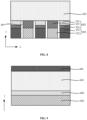
- FIG. 9 is a schematic diagram of an overall structure of a solar cell.
- the structures of solar cell in the above embodiments of the present disclosure are illustrated based on an IBC solar cell.
- the solar cell may also be a TOPCon solar cell.
- a tunneling layer 402 is formed on a rear surface of a substrate 401, and a doped conductive layer 403 is formed on the tunneling layer 402.
- One or more emitters 404 are formed on a front surface of the substrate 401.
- the doping type of the doped conductive layer 403 is the same as the doping type of the substrate 401, and a doping type of the one or more emitters 404 is different from that of the substrate 401. That is to say, the substrate 401 and the doped conductive layer 403 both have first dopant atoms, and the one or more emitters 404 have second dopant atoms.
- the atomic percentage of the first dopant atoms in the doped conductive layer 403 is higher than the atomic percentage of the first dopant atoms in the substrate 401, and is lower than the atomic percentage of the first dopant atoms in the tunneling layer 402. That is to say, enrichment of the first dopant atoms can be achieved in the tunneling layer 402 formed on the rear surface of the TOPCon solar cell, thereby improving the passivation effect and increasing the open-circuit voltage of the TOPCon solar cell.
- a ratio of the atomic percentage of the first dopant atoms in the tunneling layer 402 to the atomic percentage of the first dopant atoms in the doped conductive layer 403 ranges from 1 to 5, such as 1.1, 1.2, 1.35, 1.5, 1.75, 2, 2.4, 2.8, 3.25, 3.75, 4.5, 4.85, or the like.
- the atomic percentage of the first dopant atoms in the doped conductive layer 403 ranges from 0.2% to 5%, such as 0.25%, 0.5%, 0.8%, 1.2%, 1.5%, 1.8%, 2.25%, 2.75%, 3.5%, 4.5%, or the like.
- the atomic percentage of the first dopant atoms in the doped conductive layer 403 reduces in gradient in a direction perpendicular to the rear surface of the substrate 401 and away from the substrate 401.
- the atomic percentage of the first dopant atoms in the tunneling layer 402 ranges from 1% to 10%, such as 1.25%, 1.5%, 2%, 2.5%, 3.5%, 5%, 6.5%, 8%, 9.5%, or the like.
- the substrate 410 in the TOPCon solar cell is similar to the substrate 101 in the IBC solar cell, and thus will not be described here.
- the doped conductive layer 403 in the TOPCon solar cell may be analogous to the first doped regions 131 in the IBC solar cell
- the tunneling layer 402 in the TOPCon solar cell may be analogous to the first regions 121 in the IBC solar cell
- the one or more emitters 404 in the TOPCon solar cell may be analogous to the second doped regions 132 in the IBC solar cell.
- the material of the doped conductive layer 403 is similar to the material of the first doped regions 131
- the material of the tunneling layer 402 is similar to the material of the first regions 121, and details are not described here.
- the material of the one or more emitters 404 may be similar to the material of the substrate 401, and may also include at least one of aluminum oxide, silicon oxide and silicon nitride.
- FIG. 10 is a schematic diagram of an overall structure of one more solar cell, where a direction Y represents a direction perpendicular to the rear surface of the substrate 401.
- the tunneling layer 402 includes a first portion 421 contacting with the substrate 401, and the atomic percentage of the first dopant atoms in the first portion 421 is higher than the atomic percentage of the first dopant atoms in the tunneling layer 402,
- the atomic percentage of the first dopant atoms in the tunneling layer 402 refers to the average atomic percentage of the first dopant atoms in the tunneling layer 402 including the first portion 421.
- the tunneling layer 402 may be regarded as being formed by the first portion 421 and the other portion except for the first portion 421, and the doping concentration of the doped element in the first portion 421 is higher than the doping concentration of the doped element in the other portion except for the first portion 421 of the tunneling layer 402.
- a ratio of the thickness of the first portion 421 to the thickness of the tunneling layer 402 ranges from 0.25 to 0.5, such as 0.275, 0.3, 0.325, 0.375, 0.425, 0.45, or the like.
- the thickness of the first portion 421 in the direction perpendicular to the rear surface of the substrate 401 ranges from 0.25 nm to 1 nm, such as 0.3 nm, 0.35 nm, 0.5 nm, 0.7 nm, 0.9 nm, or the like.
- FIG. 11 is a schematic diagram of an overall structure of one more solar cell, where a direction Y represents the direction perpendicular to the rear surface of the substrate 401.
- the tunneling layer 402 includes a second portion 422 contacting with the doped conductive layer 403, and the atomic percentage of the first dopant atoms in the second portion 422 is higher than the atomic percentage of the first dopant atoms in the tunneling layer 402.
- the atomic percentage of the first dopant atoms in the tunneling layer 402 refers to the average atomic percentage of the first dopant atoms in the tunneling layer 402 including the second portion 422.
- the tunneling layer 402 may be regarded as being formed by the second portion 422 and the other portion except for the second portion 422, and the doping concentration of the doped element in the second portion 422 is higher than the doping concentration of the doped element in the other portion except for the second portion 422 of the tunneling layer 402.
- the features in the above embodiments may not only exist separately in the solar cell, but also can be implemented in combination with each other without technical conflicts and without departing from the inventive concept of the embodiments of the present disclosure.
- some embodiments take the IBC solar cell as examples, and some embodiments take the TOPCon solar cell as examples for description.
- the features applied to one type of solar cell in the embodiments may also be combined and applied to another type of solar cell, which will not be described in detail in the embodiments of the present disclosure.
- some embodiments of the present disclosure provide a solar cell, a passivation contact structure formed by a tunneling layer and a doped conductive layer is disposed on a rear surface of a substrate of the solar cell, which can significantly reduce recombination of carriers occurred on the rear surface of the substrate, thereby reducing the recombination current on the rear surface of the substrate, and reducing the carrier recombination loss of the solar cell.
- the tunneling layer is formed by first regions and second regions, the first regions interleave with the second regions in a first direction, each first doped region of the first doped regions is formed on a respective first region of the first regions, each first region and each first doped region include first dopant atoms, and the atomic percentage of the first dopant atoms in the first regions is higher than the atomic percentage of the first dopant atoms in the first doped regions. Because of the enrichment of the first dopant atoms in the tunneling layer, the open-circuit voltage of the solar cell can be further increased, thereby reducing the carrier recombination loss, and improving the photoelectric conversion efficiency of the solar cell.
- the plurality of cell strings 1101 may be electrically connected by conductive strips 1104.
- the encapsulation layers 1102 cover front surfaces and rear surfaces of the solar cells.
- the encapsulation layers 1102 may be an organic encapsulation adhesive film such as an ethylene-vinyl acetate copolymer (EVA) adhesive film, a polyethylene octene co-elastomer (POE) adhesive film, or a polyethylene terephthalate (PET) adhesive film.
- EVA ethylene-vinyl acetate copolymer
- POE polyethylene octene co-elastomer
- PET polyethylene terephthalate
- the at least one cover plate 1103 may be a glass cover plate, a plastic cover plate, or the like that has a light transmission function.
- a surface of the at least one cover plate 1103 facing to the encapsulation layers 1102 may be a textured surface, thereby increasing the utilization rate of incident light.
Landscapes
- Photovoltaic Devices (AREA)
Applications Claiming Priority (1)
| Application Number | Priority Date | Filing Date | Title |
|---|---|---|---|
| CN202311846847.7A CN117690982A (zh) | 2023-12-28 | 2023-12-28 | 太阳能电池及光伏组件 |
Publications (1)
| Publication Number | Publication Date |
|---|---|
| EP4579762A1 true EP4579762A1 (de) | 2025-07-02 |
Family
ID=90135360
Family Applications (1)
| Application Number | Title | Priority Date | Filing Date |
|---|---|---|---|
| EP24162248.9A Pending EP4579762A1 (de) | 2023-12-28 | 2024-03-08 | Solarzelle und fotovoltaisches modul |
Country Status (4)
| Country | Link |
|---|---|
| US (1) | US20250221085A1 (de) |
| EP (1) | EP4579762A1 (de) |
| JP (2) | JP2025105379A (de) |
| CN (1) | CN117690982A (de) |
Citations (4)
| Publication number | Priority date | Publication date | Assignee | Title |
|---|---|---|---|---|
| US20150380599A1 (en) * | 2014-06-30 | 2015-12-31 | David D. Smith | Solar cell emitter region fabrication using ion implantation |
| CN210200743U (zh) * | 2019-06-24 | 2020-03-27 | 泰州隆基乐叶光伏科技有限公司 | 太阳能电池 |
| CN115954414A (zh) * | 2023-02-21 | 2023-04-11 | 浙江晶科能源有限公司 | 一种光伏电池及其制备方法、光伏组件 |
| US20230253520A1 (en) * | 2020-07-13 | 2023-08-10 | Semco Smartech France | Solar cell manufacture |
Family Cites Families (4)
| Publication number | Priority date | Publication date | Assignee | Title |
|---|---|---|---|---|
| US20130048070A1 (en) * | 2011-08-26 | 2013-02-28 | Arash Hazeghi | Tunnel photovoltaic |
| US20130298973A1 (en) * | 2012-05-14 | 2013-11-14 | Silevo, Inc. | Tunneling-junction solar cell with shallow counter doping layer in the substrate |
| EP3163632A1 (de) * | 2015-11-02 | 2017-05-03 | CSEM Centre Suisse d'Electronique et de Microtechnique SA - Recherche et Développement | Fotovoltaisches modul und verfahren zur herstellung davon |
| CN115995500A (zh) * | 2022-10-28 | 2023-04-21 | 天合光能股份有限公司 | 太阳能电池及其制备方法 |
-
2023
- 2023-12-28 CN CN202311846847.7A patent/CN117690982A/zh active Pending
-
2024
- 2024-03-08 US US18/600,460 patent/US20250221085A1/en active Pending
- 2024-03-08 EP EP24162248.9A patent/EP4579762A1/de active Pending
- 2024-03-15 JP JP2024040777A patent/JP2025105379A/ja active Pending
-
2025
- 2025-10-30 JP JP2025183288A patent/JP2026003096A/ja active Pending
Patent Citations (4)
| Publication number | Priority date | Publication date | Assignee | Title |
|---|---|---|---|---|
| US20150380599A1 (en) * | 2014-06-30 | 2015-12-31 | David D. Smith | Solar cell emitter region fabrication using ion implantation |
| CN210200743U (zh) * | 2019-06-24 | 2020-03-27 | 泰州隆基乐叶光伏科技有限公司 | 太阳能电池 |
| US20230253520A1 (en) * | 2020-07-13 | 2023-08-10 | Semco Smartech France | Solar cell manufacture |
| CN115954414A (zh) * | 2023-02-21 | 2023-04-11 | 浙江晶科能源有限公司 | 一种光伏电池及其制备方法、光伏组件 |
Also Published As
| Publication number | Publication date |
|---|---|
| US20250221085A1 (en) | 2025-07-03 |
| CN117690982A (zh) | 2024-03-12 |
| JP2025105379A (ja) | 2025-07-10 |
| JP2026003096A (ja) | 2026-01-08 |
Similar Documents
| Publication | Publication Date | Title |
|---|---|---|
| JP7168800B1 (ja) | 太陽電池及び光起電力モジュール | |
| US12575219B2 (en) | Solar cell and photovoltaic module | |
| US20250374711A1 (en) | Solar cell, method for preparing the same, and photovoltaic module | |
| JP7583860B2 (ja) | 太陽電池および光起電力モジュール | |
| EP4571845A1 (de) | Solarzelle, verfahren zur herstellung davon und fotovoltaisches modul | |
| US20250311480A1 (en) | Solar cell, tandem solar cell and photovoltaic module | |
| US20250311521A1 (en) | Solar cell, tandem solar cell and photovoltaic module | |
| US20250255032A1 (en) | Solar cell and photovoltaic module | |
| AU2024201762B9 (en) | Solar cell and photovoltaic module | |
| US12446389B2 (en) | Tandem cell, method for preparing the same, and photovoltaic module | |
| US20250098334A1 (en) | Solar cell and photovoltaic module | |
| US20260059867A1 (en) | Solar cell, method for manufacturing solar cell, and photovoltaic module | |
| JP7248856B1 (ja) | 太陽電池および太陽電池の製造方法、光起電力モジュール | |
| CN116913989A (zh) | 太阳能电池及光伏组件 | |
| US12593528B2 (en) | Solar cell and photovoltaic module | |
| EP0248953A1 (de) | Kaskadensolarzellen | |
| EP4579762A1 (de) | Solarzelle und fotovoltaisches modul | |
| CN119008728A (zh) | 太阳能电池及光伏组件 | |
| CN117995924A (zh) | 叠层电池以及光伏组件 |
Legal Events
| Date | Code | Title | Description |
|---|---|---|---|
| PUAI | Public reference made under article 153(3) epc to a published international application that has entered the european phase |
Free format text: ORIGINAL CODE: 0009012 |
|
| STAA | Information on the status of an ep patent application or granted ep patent |
Free format text: STATUS: REQUEST FOR EXAMINATION WAS MADE |
|
| 17P | Request for examination filed |
Effective date: 20240308 |
|
| AK | Designated contracting states |
Kind code of ref document: A1 Designated state(s): AL AT BE BG CH CY CZ DE DK EE ES FI FR GB GR HR HU IE IS IT LI LT LU LV MC ME MK MT NL NO PL PT RO RS SE SI SK SM TR |
|
| STAA | Information on the status of an ep patent application or granted ep patent |
Free format text: STATUS: EXAMINATION IS IN PROGRESS |
|
| 17Q | First examination report despatched |
Effective date: 20260121 |