EP4579944A1 - Filtre pour dispositif de communication - Google Patents
Filtre pour dispositif de communication Download PDFInfo
- Publication number
- EP4579944A1 EP4579944A1 EP23857757.1A EP23857757A EP4579944A1 EP 4579944 A1 EP4579944 A1 EP 4579944A1 EP 23857757 A EP23857757 A EP 23857757A EP 4579944 A1 EP4579944 A1 EP 4579944A1
- Authority
- EP
- European Patent Office
- Prior art keywords
- cavity
- forming panel
- filter
- resonators
- panel
- Prior art date
- Legal status (The legal status is an assumption and is not a legal conclusion. Google has not performed a legal analysis and makes no representation as to the accuracy of the status listed.)
- Pending
Links
Images


Classifications
-
- H—ELECTRICITY
- H01—ELECTRIC ELEMENTS
- H01P—WAVEGUIDES; RESONATORS, LINES, OR OTHER DEVICES OF THE WAVEGUIDE TYPE
- H01P1/00—Auxiliary devices
- H01P1/20—Frequency-selective devices, e.g. filters
- H01P1/207—Hollow waveguide filters
-
- H—ELECTRICITY
- H01—ELECTRIC ELEMENTS
- H01P—WAVEGUIDES; RESONATORS, LINES, OR OTHER DEVICES OF THE WAVEGUIDE TYPE
- H01P1/00—Auxiliary devices
- H01P1/20—Frequency-selective devices, e.g. filters
- H01P1/207—Hollow waveguide filters
- H01P1/208—Cascaded cavities; Cascaded resonators inside a hollow waveguide structure
-
- H—ELECTRICITY
- H01—ELECTRIC ELEMENTS
- H01P—WAVEGUIDES; RESONATORS, LINES, OR OTHER DEVICES OF THE WAVEGUIDE TYPE
- H01P1/00—Auxiliary devices
- H01P1/20—Frequency-selective devices, e.g. filters
- H01P1/213—Frequency-selective devices, e.g. filters combining or separating two or more different frequencies
Definitions
- the present disclosure relates to a filter for communication devices and, more particularly, to a filter for communication devices that is easy to manufacture, facilitates securing of a usable area of a main board (or power amplifier (PA) board), and prevents an increase in the size of an entire antenna device in a thickness direction.
- a main board or power amplifier (PA) board
- Radio frequency devices are typically configured with a connected structure of a plurality of resonators.
- Such resonators are circuit elements that resonate at specific frequencies through a combination of an inductor (L) and a capacitor (C) in terms of equivalent electronic circuits.
- Each resonator has a structure in which a dielectric resonance element (DR) or a metallic resonance element is installed in a cavity, such as a metallic cylindrical or rectangular parallelopiped cavity enclosed by conductors. Accordingly, each resonator allows only an electromagnetic field of a unique frequency corresponding to a processing frequency band to exist within the associated cavity, thereby enabling high-frequency resonance.
- the resonator has a multi-stage structure in which a plurality of cavities are used to form a plurality of resonant stages, and the plurality of resonant stages are sequentially connected.
- An example of a radio frequency filter having a multicavity structure may include the invention disclosed in Korean Patent Application Laid-Open No. 10-2004-0100084 (Title: "Radio frequency filter,” Publication Date: December 2, 2004 ), which was previously filed by the present applicant.
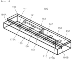
- a filter for communication devices may include a base plate made of a conductive material, and manufactured in an unfolded state, the base plate being configured foldable such that, upon folding, a cavity is formed inside while simultaneously positioning a plurality of resonators to protrude by a set length in a thickness direction or a width direction in the cavity.
- the plurality of resonators may each have a distal end portion having a wider width than a remaining portion, and include a resonance characteristic end formed by curling opposite widthwise ends of the distal end portion in a rounded shape in one thickness direction from a leading end of the remaining portion.
- the embodiment of the filter for communication devices according to the present disclosure is not necessarily limited to the aforementioned first embodiment 100, as long as the cavity C is formed through a process of folding the base plate 105.
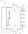
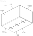
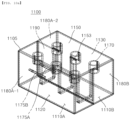
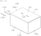
- a filter 1100 for communication devices according to a second embodiment of the present disclosure will be described in detail.
- the body bottom forming panel 110 that forms the bottom of the cavity C is formed as a single integrated panel.
- the body bottom forming panels that form the bottom of the cavity C are provided as two separate panels 1110A and 1110B in the width direction of the cavity C.
- the plurality of resonators 1170 may be integrally formed on one end of each of the separated body bottom forming panels 1110A and 1110B so as to be foldable in the thickness direction of the cavity C from the one end of each of the body bottom forming panels 1110A and 1110B, without requiring a separate resonator panel.
- the first-side thickness forming panel 120 and the second-side thickness forming panel 130 extend from the first widthwise end and the second widthwise end of the body bottom forming panel 110, respectively, and the first-side shielding panel 180A and the second-side shielding panel 180B extend from the first longitudinal end and the second longitudinal end of the body bottom forming panel 110, respectively.
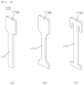
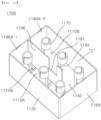
- a plurality of resonators 1170 which are integrally formed with the body bottom forming panels 1110A and 1110B, may each include a resonance characteristic end 1173 formed in such a way that a distal end portion of a resonance bar 1171 has a wider width than a remaining portion and opposite widthwise ends of the distal end portion are curled in a rounded shape in one thickness direction from a leading end of the remaining portion.
- the opposite widthwise ends in a rounded state may be spaced apart from each other by a predetermined distance.
- the resonance characteristic ends 1173A of the plurality of resonators 1170 may each be formed to have at least one circular horizontal cross-section (refer to (b) in FIG. 14 ) or semicircular horizontal cross-section (refer to (a) in FIG. 14 ).
- the input terminal pin 175A and the output terminal pin 175B are each integrally formed with one of the resonators 170 and then fixedly installed by penetrating the corresponding one of the input port installation portion 115A and the output port installation portion 115B formed in the body bottom forming panel 110 during the folding process.
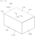
- an input terminal pin 1175A and an output terminal pin 1175B are provided as separate elements and fixedly installed by penetrating the input port installation portion 1115A formed in the first first-side shielding panel 1180A-1 and the output port installation portion 1115B formed in the second first-side shielding panel 1180A-2, respectively.
- the input terminal pin 1175A may be connected to an input port formed in an unillustrated main board and to one of the plurality of resonators 1170 so that a signal transmitted from the input port is received.
- the output terminal pin 1175B may be connected to an output port formed in the unillustrated main board and to one of the plurality of resonators 1170 so that a signal is transmitted to the output port and then output.
- the present disclosure provides a filter for communication devices that can eliminate conventional joining processes for forming a cavity and providing structures such as resonators within the cavity, thereby reducing insertion loss caused by coupling of two physical structures.
Landscapes
- Control Of Motors That Do Not Use Commutators (AREA)
Applications Claiming Priority (3)
| Application Number | Priority Date | Filing Date | Title |
|---|---|---|---|
| KR20220107873 | 2022-08-26 | ||
| KR1020230110841A KR20240029523A (ko) | 2022-08-26 | 2023-08-23 | 통신기기용 필터 |
| PCT/KR2023/012581 WO2024043725A1 (fr) | 2022-08-26 | 2023-08-24 | Filtre pour dispositif de communication |
Publications (1)
| Publication Number | Publication Date |
|---|---|
| EP4579944A1 true EP4579944A1 (fr) | 2025-07-02 |
Family
ID=90013788
Family Applications (1)
| Application Number | Title | Priority Date | Filing Date |
|---|---|---|---|
| EP23857757.1A Pending EP4579944A1 (fr) | 2022-08-26 | 2023-08-24 | Filtre pour dispositif de communication |
Country Status (5)
| Country | Link |
|---|---|
| US (1) | US20250192411A1 (fr) |
| EP (1) | EP4579944A1 (fr) |
| JP (1) | JP2025527622A (fr) |
| CN (1) | CN120092364A (fr) |
| WO (1) | WO2024043725A1 (fr) |
Family Cites Families (9)
| Publication number | Priority date | Publication date | Assignee | Title |
|---|---|---|---|---|
| JPS55100701A (en) * | 1979-01-26 | 1980-07-31 | Matsushita Electric Ind Co Ltd | Coaxial resonator |
| JPH0714123B2 (ja) * | 1987-01-30 | 1995-02-15 | 株式会社日立製作所 | 導波管フイルタ |
| KR100489698B1 (ko) | 2003-05-21 | 2005-05-17 | 주식회사 케이엠더블유 | 무선 주파수 필터 |
| KR100844163B1 (ko) * | 2007-03-15 | 2008-07-04 | 주식회사 케이엠더블유 | 다중노치필터 |
| JP2009218662A (ja) * | 2008-03-07 | 2009-09-24 | Panasonic Corp | フィルタ装置 |
| KR20100100117A (ko) * | 2009-03-05 | 2010-09-15 | 주식회사 이롬테크 | 초소형 무선 고주파 필터 |
| KR101615095B1 (ko) * | 2014-03-11 | 2016-04-26 | 주식회사 웨이브일렉트로닉스 | 수직 또는 수평 방향으로 교차하는 격벽 구조를 포함하는 공진기 및 이를 이용한 필터 |
| JP2016184831A (ja) * | 2015-03-25 | 2016-10-20 | 古河電気工業株式会社 | 誘導性アイリス結合導波管フィルタ |
| KR101939989B1 (ko) * | 2018-08-01 | 2019-01-18 | 주식회사 엘트로닉스 | 고주파 필터 |
-
2023
- 2023-08-24 EP EP23857757.1A patent/EP4579944A1/fr active Pending
- 2023-08-24 WO PCT/KR2023/012581 patent/WO2024043725A1/fr not_active Ceased
- 2023-08-24 CN CN202380061109.3A patent/CN120092364A/zh active Pending
- 2023-08-24 JP JP2025511311A patent/JP2025527622A/ja active Pending
-
2025
- 2025-02-22 US US19/060,638 patent/US20250192411A1/en active Pending
Also Published As
| Publication number | Publication date |
|---|---|
| US20250192411A1 (en) | 2025-06-12 |
| CN120092364A (zh) | 2025-06-03 |
| WO2024043725A1 (fr) | 2024-02-29 |
| JP2025527622A (ja) | 2025-08-22 |
Similar Documents
| Publication | Publication Date | Title |
|---|---|---|
| WO1994002971A1 (fr) | Filtre dielectrique et son blindage | |
| EP4579944A1 (fr) | Filtre pour dispositif de communication | |
| EP4579945A1 (fr) | Filtre pour dispositif de communication | |
| EP4579942A1 (fr) | Filtre pour dispositif de communication | |
| EP4579943A1 (fr) | Filtre pour dispositif de communication | |
| CN220963712U (zh) | 通信设备用滤波器 | |
| KR20240038615A (ko) | 통신기기용 필터 및 그 제조방법 | |
| KR20240029523A (ko) | 통신기기용 필터 | |
| CN220774703U (zh) | 通信设备用滤波器 | |
| US20250219276A1 (en) | Filter for communication device and manufacturing method therefor | |
| CN220963713U (zh) | 通信设备用滤波器 | |
| CN220774702U (zh) | 通信设备用滤波器 | |
| US20260039000A1 (en) | Filter for communication device | |
| EP4604316A1 (fr) | Filtre pour dispositif de communication | |
| CN221239781U (zh) | 通信设备用滤波器 | |
| KR20240029524A (ko) | 통신기기용 필터 | |
| JP7852150B2 (ja) | 通信機器用フィルタおよびその製造方法 | |
| CN220963704U (zh) | 通信设备用滤波器 | |
| EP4564590A1 (fr) | Filtre pour dispositif de communication | |
| KR20240029521A (ko) | 통신기기용 필터 | |
| KR20240029522A (ko) | 통신기기용 필터 | |
| EP4564589A1 (fr) | Filtre pour dispositif de communication | |
| CN220963711U (zh) | 通信设备用滤波器 | |
| JP2025529413A (ja) | 通信機器用フィルタ | |
| KR20240051862A (ko) | 통신기기용 필터 |
Legal Events
| Date | Code | Title | Description |
|---|---|---|---|
| STAA | Information on the status of an ep patent application or granted ep patent |
Free format text: STATUS: THE INTERNATIONAL PUBLICATION HAS BEEN MADE |
|
| PUAI | Public reference made under article 153(3) epc to a published international application that has entered the european phase |
Free format text: ORIGINAL CODE: 0009012 |
|
| STAA | Information on the status of an ep patent application or granted ep patent |
Free format text: STATUS: REQUEST FOR EXAMINATION WAS MADE |
|
| 17P | Request for examination filed |
Effective date: 20250325 |
|
| AK | Designated contracting states |
Kind code of ref document: A1 Designated state(s): AL AT BE BG CH CY CZ DE DK EE ES FI FR GB GR HR HU IE IS IT LI LT LU LV MC ME MK MT NL NO PL PT RO RS SE SI SK SM TR |
|
| DAV | Request for validation of the european patent (deleted) | ||
| DAX | Request for extension of the european patent (deleted) |