EP4579986A1 - Vorrichtung zur verarbeitung eines batteriepacks und elektronische vorrichtung - Google Patents
Vorrichtung zur verarbeitung eines batteriepacks und elektronische vorrichtung Download PDFInfo
- Publication number
- EP4579986A1 EP4579986A1 EP23866684.6A EP23866684A EP4579986A1 EP 4579986 A1 EP4579986 A1 EP 4579986A1 EP 23866684 A EP23866684 A EP 23866684A EP 4579986 A1 EP4579986 A1 EP 4579986A1
- Authority
- EP
- European Patent Office
- Prior art keywords
- chip
- pin
- battery pack
- electrically connected
- effect transistor
- Prior art date
- Legal status (The legal status is an assumption and is not a legal conclusion. Google has not performed a legal analysis and makes no representation as to the accuracy of the status listed.)
- Pending
Links
Images




Classifications
-
- H—ELECTRICITY
- H02—GENERATION; CONVERSION OR DISTRIBUTION OF ELECTRIC POWER
- H02J—ELECTRIC POWER NETWORKS; CIRCUIT ARRANGEMENTS OR SYSTEMS FOR SUPPLYING OR DISTRIBUTING ELECTRIC POWER; SYSTEMS FOR STORING ELECTRIC ENERGY
- H02J7/00—Circuit arrangements for charging or discharging batteries or for supplying loads from batteries
- H02J7/50—Circuit arrangements for charging or discharging batteries or for supplying loads from batteries acting upon multiple batteries simultaneously or sequentially
-
- H—ELECTRICITY
- H02—GENERATION; CONVERSION OR DISTRIBUTION OF ELECTRIC POWER
- H02J—ELECTRIC POWER NETWORKS; CIRCUIT ARRANGEMENTS OR SYSTEMS FOR SUPPLYING OR DISTRIBUTING ELECTRIC POWER; SYSTEMS FOR STORING ELECTRIC ENERGY
- H02J7/00—Circuit arrangements for charging or discharging batteries or for supplying loads from batteries
- H02J7/865—Battery or charger load switching, e.g. concurrent charging and load supply
-
- H—ELECTRICITY
- H02—GENERATION; CONVERSION OR DISTRIBUTION OF ELECTRIC POWER
- H02J—ELECTRIC POWER NETWORKS; CIRCUIT ARRANGEMENTS OR SYSTEMS FOR SUPPLYING OR DISTRIBUTING ELECTRIC POWER; SYSTEMS FOR STORING ELECTRIC ENERGY
- H02J7/00—Circuit arrangements for charging or discharging batteries or for supplying loads from batteries
- H02J7/40—Circuit arrangements for charging or discharging batteries or for supplying loads from batteries characterised by the exchange of charge or discharge related data
-
- H—ELECTRICITY
- H02—GENERATION; CONVERSION OR DISTRIBUTION OF ELECTRIC POWER
- H02J—ELECTRIC POWER NETWORKS; CIRCUIT ARRANGEMENTS OR SYSTEMS FOR SUPPLYING OR DISTRIBUTING ELECTRIC POWER; SYSTEMS FOR STORING ELECTRIC ENERGY
- H02J7/00—Circuit arrangements for charging or discharging batteries or for supplying loads from batteries
- H02J7/40—Circuit arrangements for charging or discharging batteries or for supplying loads from batteries characterised by the exchange of charge or discharge related data
- H02J7/44—Circuit arrangements for charging or discharging batteries or for supplying loads from batteries characterised by the exchange of charge or discharge related data between battery management systems and power sources
-
- H—ELECTRICITY
- H02—GENERATION; CONVERSION OR DISTRIBUTION OF ELECTRIC POWER
- H02J—ELECTRIC POWER NETWORKS; CIRCUIT ARRANGEMENTS OR SYSTEMS FOR SUPPLYING OR DISTRIBUTING ELECTRIC POWER; SYSTEMS FOR STORING ELECTRIC ENERGY
- H02J7/00—Circuit arrangements for charging or discharging batteries or for supplying loads from batteries
- H02J7/60—Circuit arrangements for charging or discharging batteries or for supplying loads from batteries including safety or protection arrangements
-
- H—ELECTRICITY
- H02—GENERATION; CONVERSION OR DISTRIBUTION OF ELECTRIC POWER
- H02J—ELECTRIC POWER NETWORKS; CIRCUIT ARRANGEMENTS OR SYSTEMS FOR SUPPLYING OR DISTRIBUTING ELECTRIC POWER; SYSTEMS FOR STORING ELECTRIC ENERGY
- H02J7/00—Circuit arrangements for charging or discharging batteries or for supplying loads from batteries
- H02J7/60—Circuit arrangements for charging or discharging batteries or for supplying loads from batteries including safety or protection arrangements
- H02J7/663—Circuit arrangements for charging or discharging batteries or for supplying loads from batteries including safety or protection arrangements using battery or load disconnect circuits
-
- H—ELECTRICITY
- H02—GENERATION; CONVERSION OR DISTRIBUTION OF ELECTRIC POWER
- H02J—ELECTRIC POWER NETWORKS; CIRCUIT ARRANGEMENTS OR SYSTEMS FOR SUPPLYING OR DISTRIBUTING ELECTRIC POWER; SYSTEMS FOR STORING ELECTRIC ENERGY
- H02J7/00—Circuit arrangements for charging or discharging batteries or for supplying loads from batteries
- H02J7/80—Circuit arrangements for charging or discharging batteries or for supplying loads from batteries including monitoring or indicating arrangements
-
- Y—GENERAL TAGGING OF NEW TECHNOLOGICAL DEVELOPMENTS; GENERAL TAGGING OF CROSS-SECTIONAL TECHNOLOGIES SPANNING OVER SEVERAL SECTIONS OF THE IPC; TECHNICAL SUBJECTS COVERED BY FORMER USPC CROSS-REFERENCE ART COLLECTIONS [XRACs] AND DIGESTS
- Y02—TECHNOLOGIES OR APPLICATIONS FOR MITIGATION OR ADAPTATION AGAINST CLIMATE CHANGE
- Y02E—REDUCTION OF GREENHOUSE GAS [GHG] EMISSIONS, RELATED TO ENERGY GENERATION, TRANSMISSION OR DISTRIBUTION
- Y02E60/00—Enabling technologies; Technologies with a potential or indirect contribution to GHG emissions mitigation
- Y02E60/10—Energy storage using batteries
Definitions
- This disclosure relates to the field of battery technology, particularly to a battery pack processing device and electronic device.
- I2C Inter-Integrated Circuit
- this disclosure provides a battery pack processing device and electronic device.
- this disclosure provides a battery pack processing device, including:
- the battery pack communication circuit includes a switch module, which includes a twelfth field-effect transistor and a thirteenth field-effect transistor.
- the source of the twelfth field-effect transistor and the source of the thirteenth field-effect transistor are electrically connected to the 15th pin of the second chip;
- the second chip is used to control the conduction or disconnection of the switch module after determining whether the battery pack is connected in parallel or in series.
- the battery pack communication circuit includes a sixth chip, the 8th pin of the sixth chip is electrically connected to the 16th pin of the second chip; the 1st pin of the sixth chip is electrically connected to the 15th pin of the second chip;
- the second chip after determining whether the battery pack is connected in parallel or in series, sends an enable signal to the 1st pin of the sixth chip to activate the sixth chip;
- the sixth chip is used to send the output current value read from the sixth chip to the 15th pin of the second chip.
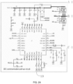
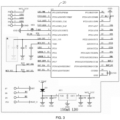
- the voltage control circuit 40 includes a third chip U3 and a fourth chip U4, the connection point of the 3rd and 5th pins of the fourth chip U4 is electrically connected to the 16th pin of the third chip U3; the 4th pin (LINKA1 signal) of the fourth chip U4 is electrically connected to the 10th pin (LINKA_1 signal) of the second chip U2; the 6th pin (LINKB signal) of the fourth chip U4 is electrically connected to the 11th pin (LINKB_1 signal) of the second chip U2.
- the 11th pin of the second chip U2 is the PT16 pin.
- the 16th pin of the third chip U3 is the FB pin.
- the 3rd and 5th pins of the fourth chip U4 are the CMPI/SDA and FB pins, respectively.
- the 4th pin of the fourth chip U4 is the SCL pin.
- the fourth chip U4 is used to determine whether a device is plugged into the charge-discharge interface 101, and if a device is plugged in, it sends the corresponding level to the second chip U2.
- the fourth chip U4 is also used to determine whether the charge-discharge is in a single-port state or a dual-port state.
- the Type C port or USB port When in a single-port state, the Type C port or USB port has a fast charging function; when in a dual-port state, the Type C port and USB port have a standard charging function.
- the Type C port charges the device end or the battery pack, with a rechargeable and dischargeable interface.
- the third chip U3 is a buck IC, responsible for outputting electrical energy to the Type C and USB ports, the Type C port outputs electrical energy to mobile phones or tablets, charging externally, and after reducing the battery voltage, outputs externally.
- the battery pack communication circuit 50 includes a switch module, which includes a twelfth field-effect transistor Q12 and a thirteenth field-effect transistor Q13, the source of the twelfth field-effect transistor Q12 and the source of the thirteenth field-effect transistor Q13 are electrically connected to the 15th pin of the second chip U2.
- the 15th pin of the second chip U2 is the PT34/AIN4/RX/DMD/CC2B pin.
- the second chip U2 is used to control the conduction or disconnection of the switch module after determining whether the battery pack is connected in parallel or in series.
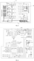
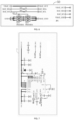
- FIG. 6 there are four signal ends VBAT_OUT, BAT-SDA, BAT-SCL, VBAT_GND, based on the information from the BAT-SDA and BAT-SCL signal ends to determine whether the battery pack is connected in parallel or in series, for example, the overall charge-discharge management circuit formed by Figures 2A and 2B , combined with Figures 3 to 6 as a whole circuit; the overall charge-discharge management circuit formed by Figures 2A and 2B , combined with Figures 3 to 5 , Figures 7 to 9 as a whole circuit; through the VBAT_OUT, BAT-SDA, BAT-SCL, VBAT_GND signal ends, the input signals from the BAT-SDA and BAT-SCL signal ends determine whether the battery pack is connected in parallel or in series. For example, if the battery is 30,000 mAh, if two are connected in parallel, there will be 60,000 mAh.
- the twelfth field-effect transistor Q12 and the thirteenth field-effect transistor Q13 are conducted, controlled by the 15th pin (PT34/AIN4/RX/DMD/CC2B pin) of the second chip U2.
- the SDA and SCL signals are default to 00, in the default state, the twelfth field-effect transistor Q12 and the thirteenth field-effect transistor Q13 are not conducting.
- the battery pack is connected in parallel, when the device is determined to be connected in reverse, the battery pack is connected in series.
- the second chip U2 normally outputs current and voltage, and the twelfth field-effect transistor Q12 and the thirteenth field-effect transistor Q13 of the switch module are conducting.
- the 8th pin of the sixth chip U6 is the IMON pin
- the 16th pin of the second chip U2 is the PT33/AIN3/TX/DPD/CC1B pin.
- the 1st pin of the sixth chip U6 is the EN pin (enable end)
- the 15th pin of the second chip U2 is the PT34/AIN4/RX/DMD/CC2B pin.
- the Bluetooth power supply module 60 includes an amplifier AU2 and a Bluetooth module BT1, the input end of the amplifier AU2 is used to receive the battery voltage VBAT_O, and the output end of the amplifier AU2 is electrically connected to the Bluetooth module BT1.
- the 1st pin of the amplifier AU2 is the GND pin
- the 2nd pin of the amplifier AU2 is the input end (VIN pin)
- the 3rd pin of the amplifier AU2 is the output end (OUT pin).
- the Bluetooth power supply module 60 is used for locating the position of the device.
- the device can be a mobile phone, tablet, or other devices waiting to be charged.
- the Bluetooth power supply module 60 can sense Bluetooth devices within a certain range and locate related devices.
- the lighting and sampling circuit 70 includes a seventh chip U7, where pin 6 of the seventh chip U7 is electrically connected to pin 27 of the second chip U2.
- pin 6 of the seventh chip U7 is the OUT pin
- pin 27 of the second chip U2 is the PT24/AIN12/DMB pin.
- the lighting and sampling circuit 70 is used to detect the presence of a load.
- the lighting and sampling circuit 70 can be used as a flashlight for illumination.
- the electrical connection between pin 6 (OUT pin) of the seventh chip U7 and pin 27 (PT24/AIN12/DMB pin) of the second chip U2 allows for the detection of current Qi-I at pin 6 of the seventh chip U7 to determine the presence of a load. Based on the presence of a load, it is determined whether the indicator light needs to be illuminated.
- the first chip U1, the second chip U2, the third chip U3, the fourth chip U4, the fifth chip U5, the sixth chip U6, and the seventh chip U7 are chips with corresponding pins that can perform corresponding functions.
- the battery pack processing device 1 includes a charge-discharge management circuit 10 comprising a first chip and a charge-discharge interface 101, where the first chip is electrically connected to the charge-discharge interface 101; a logic control circuit 20 includes a second chip; pin 11 of the first chip is electrically connected to pin 24 of the second chip; pin 12 of the first chip is electrically connected to pin 23 of the second chip; a battery pack protection circuit 30 includes a fifth chip, a lithium battery protection circuit 301, and a battery pack shutdown protection circuit 302, where the positive pole of the battery pack is electrically connected to pin 1 of the fifth chip, and the negative pole of the battery pack is electrically connected through the lithium battery protection circuit to pin 11, the CO pin, and pin 9 of the fifth chip; the first signal output end of the battery pack communication circuit 50 is electrically connected to pin 13 of the second chip; the second signal output end of the battery pack communication circuit 50 is electrically connected to pin 13 of the second chip; the battery pack communication circuit 50 is used to send control signals to the second chip through
- the present disclosure provides an electronic device that includes the battery pack processing device provided in Embodiment 1.
- the electronic device provided in this embodiment includes the battery pack processing device 1 provided in Embodiment 1, which can achieve the processing process of the battery pack processing device 1 of Embodiment 1 and can reach the corresponding effects of the battery pack processing device 1 of Embodiment 1. To avoid repetition, it is not elaborated here.
- the battery pack processing device and electronic device of the present disclosure are reproducible and can be used in various industrial applications.
- the battery pack processing device and electronic device of the present disclosure can be applied in the field of battery technology.
Landscapes
- Engineering & Computer Science (AREA)
- Power Engineering (AREA)
- Charge And Discharge Circuits For Batteries Or The Like (AREA)
- Secondary Cells (AREA)
Applications Claiming Priority (2)
| Application Number | Priority Date | Filing Date | Title |
|---|---|---|---|
| CN202311412338.3A CN117154897B (zh) | 2023-10-30 | 2023-10-30 | 电池组的处理装置和电子设备 |
| PCT/CN2023/133372 WO2025091587A1 (zh) | 2023-10-30 | 2023-11-22 | 电池组的处理装置和电子设备 |
Publications (2)
| Publication Number | Publication Date |
|---|---|
| EP4579986A1 true EP4579986A1 (de) | 2025-07-02 |
| EP4579986A4 EP4579986A4 (de) | 2025-07-16 |
Family
ID=95483085
Family Applications (1)
| Application Number | Title | Priority Date | Filing Date |
|---|---|---|---|
| EP23866684.6A Pending EP4579986A4 (de) | 2023-10-30 | 2023-11-22 | Vorrichtung zur verarbeitung eines batteriepacks und elektronische vorrichtung |
Country Status (3)
| Country | Link |
|---|---|
| US (1) | US20250141253A1 (de) |
| EP (1) | EP4579986A4 (de) |
| JP (1) | JP7788548B2 (de) |
Family Cites Families (4)
| Publication number | Priority date | Publication date | Assignee | Title |
|---|---|---|---|---|
| CN113783239B (zh) * | 2020-06-09 | 2026-04-28 | 中兴通讯股份有限公司 | 混联电池充放电方法及混联电池系统 |
| CN212726500U (zh) * | 2020-06-09 | 2021-03-16 | 中兴通讯股份有限公司 | 混联电池系统 |
| CN111682621B (zh) * | 2020-06-29 | 2024-12-31 | 宁波锂想电子有限公司 | 一种可变压锂电池组的保护电路 |
| CN114256896A (zh) * | 2020-09-23 | 2022-03-29 | 天佑电器(苏州)有限公司 | 电池包、直流工具及直流工具组件 |
-
2023
- 2023-11-22 EP EP23866684.6A patent/EP4579986A4/de active Pending
- 2023-11-22 JP JP2024524498A patent/JP7788548B2/ja active Active
-
2024
- 2024-08-23 US US18/814,413 patent/US20250141253A1/en active Pending
Also Published As
| Publication number | Publication date |
|---|---|
| EP4579986A4 (de) | 2025-07-16 |
| JP2025538058A (ja) | 2025-11-26 |
| JP7788548B2 (ja) | 2025-12-18 |
| US20250141253A1 (en) | 2025-05-01 |
Similar Documents
| Publication | Publication Date | Title |
|---|---|---|
| US8649827B2 (en) | Power supply unit for mobile terminal and power supply switching method for mobile terminal | |
| EP2480043B1 (de) | Verfahren und vorrichtung zur identifizierung eines rechnereinsatzes oder eines ladegeräteeinsatzes in einem mobilen endgerät | |
| CN204407954U (zh) | 多输入输出快充移动电源 | |
| CN203491742U (zh) | 一种移动电源电路及移动电源 | |
| CN111682621B (zh) | 一种可变压锂电池组的保护电路 | |
| CN115001069A (zh) | 一种针对同口应用的电池保护芯片的充电器检测电路 | |
| WO2022218220A1 (zh) | 充放电电路和电子设备 | |
| CN103427821B (zh) | 实现零待机电流的电源管理装置 | |
| TWI879591B (zh) | 電池組的處理裝置和電子設備 | |
| US10819130B2 (en) | Mobile charge/discharge device | |
| WO2019071388A1 (zh) | 电池控制电路及电子设备 | |
| EP4579986A1 (de) | Vorrichtung zur verarbeitung eines batteriepacks und elektronische vorrichtung | |
| CN106451693A (zh) | 充电宝及otg数据线 | |
| CN113422411A (zh) | Pd充电电路及pos机 | |
| US20240297521A1 (en) | Charging circuit and terminal device | |
| TWM624994U (zh) | 開關電源系統及其功率傳輸協定晶片 | |
| CN116667473B (zh) | 一种控制电路、电路控制方法和电子设备 | |
| WO2016182092A1 (ko) | 충방전기능을 갖는 휴대단말용 배터리팩 파우치 장치 | |
| CN208062815U (zh) | 一种锂电池电路和装置 | |
| CN209730840U (zh) | 一种快速充放电移动电源及其系统 | |
| CN202916420U (zh) | 一种移动电源的电量侦测电路 | |
| CN202019036U (zh) | 一种太阳能手机电池结构 | |
| CN224082010U (zh) | 基于Type-C的供电控制电路及Type-C切换器 | |
| CN217935139U (zh) | 一种蓝牙串口透传调试工具电路 | |
| CN218276451U (zh) | 一种电荷泵芯片以及移动终端 |
Legal Events
| Date | Code | Title | Description |
|---|---|---|---|
| STAA | Information on the status of an ep patent application or granted ep patent |
Free format text: STATUS: UNKNOWN |
|
| STAA | Information on the status of an ep patent application or granted ep patent |
Free format text: STATUS: THE INTERNATIONAL PUBLICATION HAS BEEN MADE |
|
| PUAI | Public reference made under article 153(3) epc to a published international application that has entered the european phase |
Free format text: ORIGINAL CODE: 0009012 |
|
| STAA | Information on the status of an ep patent application or granted ep patent |
Free format text: STATUS: REQUEST FOR EXAMINATION WAS MADE |
|
| STAA | Information on the status of an ep patent application or granted ep patent |
Free format text: STATUS: EXAMINATION IS IN PROGRESS |
|
| 17P | Request for examination filed |
Effective date: 20240328 |
|
| AK | Designated contracting states |
Kind code of ref document: A1 Designated state(s): AL AT BE BG CH CY CZ DE DK EE ES FI FR GB GR HR HU IE IS IT LI LT LU LV MC ME MK MT NL NO PL PT RO RS SE SI SK SM TR |
|
| A4 | Supplementary search report drawn up and despatched |
Effective date: 20250616 |
|
| RIC1 | Information provided on ipc code assigned before grant |
Ipc: H02J 7/00 20060101AFI20250610BHEP |
|
| 17Q | First examination report despatched |
Effective date: 20250630 |