EP4580030A1 - Onduleur photovoltaïque et son procédé de commande - Google Patents
Onduleur photovoltaïque et son procédé de commande Download PDFInfo
- Publication number
- EP4580030A1 EP4580030A1 EP23864443.9A EP23864443A EP4580030A1 EP 4580030 A1 EP4580030 A1 EP 4580030A1 EP 23864443 A EP23864443 A EP 23864443A EP 4580030 A1 EP4580030 A1 EP 4580030A1
- Authority
- EP
- European Patent Office
- Prior art keywords
- voltage
- conversion circuit
- photovoltaic inverter
- signal
- order harmonic
- Prior art date
- Legal status (The legal status is an assumption and is not a legal conclusion. Google has not performed a legal analysis and makes no representation as to the accuracy of the status listed.)
- Pending
Links
Images


Classifications
-
- H—ELECTRICITY
- H02—GENERATION; CONVERSION OR DISTRIBUTION OF ELECTRIC POWER
- H02M—APPARATUS FOR CONVERSION BETWEEN AC AND AC, BETWEEN AC AND DC, OR BETWEEN DC AND DC, AND FOR USE WITH MAINS OR SIMILAR POWER SUPPLY SYSTEMS; CONVERSION OF DC OR AC INPUT POWER INTO SURGE OUTPUT POWER; CONTROL OR REGULATION THEREOF
- H02M7/00—Conversion of AC power input into DC power output; Conversion of DC power input into AC power output
- H02M7/42—Conversion of DC power input into AC power output without possibility of reversal
- H02M7/44—Conversion of DC power input into AC power output without possibility of reversal by static converters
- H02M7/48—Conversion of DC power input into AC power output without possibility of reversal by static converters using discharge tubes with control electrode or semiconductor devices with control electrode
- H02M7/53—Conversion of DC power input into AC power output without possibility of reversal by static converters using discharge tubes with control electrode or semiconductor devices with control electrode using devices of a triode or transistor type requiring continuous application of a control signal
- H02M7/537—Conversion of DC power input into AC power output without possibility of reversal by static converters using discharge tubes with control electrode or semiconductor devices with control electrode using devices of a triode or transistor type requiring continuous application of a control signal using semiconductor devices only, e.g. single switched pulse inverters
- H02M7/5387—Conversion of DC power input into AC power output without possibility of reversal by static converters using discharge tubes with control electrode or semiconductor devices with control electrode using devices of a triode or transistor type requiring continuous application of a control signal using semiconductor devices only, e.g. single switched pulse inverters in a bridge configuration
- H02M7/53871—Conversion of DC power input into AC power output without possibility of reversal by static converters using discharge tubes with control electrode or semiconductor devices with control electrode using devices of a triode or transistor type requiring continuous application of a control signal using semiconductor devices only, e.g. single switched pulse inverters in a bridge configuration with automatic control of output voltage or current
-
- H—ELECTRICITY
- H02—GENERATION; CONVERSION OR DISTRIBUTION OF ELECTRIC POWER
- H02M—APPARATUS FOR CONVERSION BETWEEN AC AND AC, BETWEEN AC AND DC, OR BETWEEN DC AND DC, AND FOR USE WITH MAINS OR SIMILAR POWER SUPPLY SYSTEMS; CONVERSION OF DC OR AC INPUT POWER INTO SURGE OUTPUT POWER; CONTROL OR REGULATION THEREOF
- H02M1/00—Details of apparatus for conversion
- H02M1/0003—Details of control, feedback or regulation circuits
- H02M1/0025—Arrangements for modifying reference values, feedback values or error values in the control loop of a converter
-
- H—ELECTRICITY
- H02—GENERATION; CONVERSION OR DISTRIBUTION OF ELECTRIC POWER
- H02M—APPARATUS FOR CONVERSION BETWEEN AC AND AC, BETWEEN AC AND DC, OR BETWEEN DC AND DC, AND FOR USE WITH MAINS OR SIMILAR POWER SUPPLY SYSTEMS; CONVERSION OF DC OR AC INPUT POWER INTO SURGE OUTPUT POWER; CONTROL OR REGULATION THEREOF
- H02M1/00—Details of apparatus for conversion
- H02M1/08—Circuits specially adapted for the generation of control voltages for semiconductor devices incorporated in static converters
- H02M1/088—Circuits specially adapted for the generation of control voltages for semiconductor devices incorporated in static converters for the simultaneous control of series or parallel connected semiconductor devices
-
- H—ELECTRICITY
- H02—GENERATION; CONVERSION OR DISTRIBUTION OF ELECTRIC POWER
- H02M—APPARATUS FOR CONVERSION BETWEEN AC AND AC, BETWEEN AC AND DC, OR BETWEEN DC AND DC, AND FOR USE WITH MAINS OR SIMILAR POWER SUPPLY SYSTEMS; CONVERSION OF DC OR AC INPUT POWER INTO SURGE OUTPUT POWER; CONTROL OR REGULATION THEREOF
- H02M1/00—Details of apparatus for conversion
- H02M1/12—Arrangements for reducing harmonics from AC input or output
-
- H—ELECTRICITY
- H02—GENERATION; CONVERSION OR DISTRIBUTION OF ELECTRIC POWER
- H02M—APPARATUS FOR CONVERSION BETWEEN AC AND AC, BETWEEN AC AND DC, OR BETWEEN DC AND DC, AND FOR USE WITH MAINS OR SIMILAR POWER SUPPLY SYSTEMS; CONVERSION OF DC OR AC INPUT POWER INTO SURGE OUTPUT POWER; CONTROL OR REGULATION THEREOF
- H02M7/00—Conversion of AC power input into DC power output; Conversion of DC power input into AC power output
- H02M7/42—Conversion of DC power input into AC power output without possibility of reversal
- H02M7/44—Conversion of DC power input into AC power output without possibility of reversal by static converters
- H02M7/48—Conversion of DC power input into AC power output without possibility of reversal by static converters using discharge tubes with control electrode or semiconductor devices with control electrode
- H02M7/483—Converters with outputs that each can have more than two voltages levels
- H02M7/4833—Capacitor voltage balancing
-
- H—ELECTRICITY
- H02—GENERATION; CONVERSION OR DISTRIBUTION OF ELECTRIC POWER
- H02M—APPARATUS FOR CONVERSION BETWEEN AC AND AC, BETWEEN AC AND DC, OR BETWEEN DC AND DC, AND FOR USE WITH MAINS OR SIMILAR POWER SUPPLY SYSTEMS; CONVERSION OF DC OR AC INPUT POWER INTO SURGE OUTPUT POWER; CONTROL OR REGULATION THEREOF
- H02M7/00—Conversion of AC power input into DC power output; Conversion of DC power input into AC power output
- H02M7/42—Conversion of DC power input into AC power output without possibility of reversal
- H02M7/44—Conversion of DC power input into AC power output without possibility of reversal by static converters
- H02M7/48—Conversion of DC power input into AC power output without possibility of reversal by static converters using discharge tubes with control electrode or semiconductor devices with control electrode
- H02M7/483—Converters with outputs that each can have more than two voltages levels
- H02M7/487—Neutral point clamped inverters
-
- H—ELECTRICITY
- H02—GENERATION; CONVERSION OR DISTRIBUTION OF ELECTRIC POWER
- H02S—GENERATION OF ELECTRIC POWER BY CONVERSION OF INFRARED RADIATION, VISIBLE LIGHT OR ULTRAVIOLET LIGHT, e.g. USING PHOTOVOLTAIC [PV] MODULES
- H02S40/00—Components or accessories in combination with PV modules, not provided for in groups H02S10/00 - H02S30/00
- H02S40/30—Electrical components
- H02S40/32—Electrical components comprising DC/AC inverter means associated with the PV module itself, e.g. AC modules
-
- Y—GENERAL TAGGING OF NEW TECHNOLOGICAL DEVELOPMENTS; GENERAL TAGGING OF CROSS-SECTIONAL TECHNOLOGIES SPANNING OVER SEVERAL SECTIONS OF THE IPC; TECHNICAL SUBJECTS COVERED BY FORMER USPC CROSS-REFERENCE ART COLLECTIONS [XRACs] AND DIGESTS
- Y02—TECHNOLOGIES OR APPLICATIONS FOR MITIGATION OR ADAPTATION AGAINST CLIMATE CHANGE
- Y02E—REDUCTION OF GREENHOUSE GAS [GHG] EMISSIONS, RELATED TO ENERGY GENERATION, TRANSMISSION OR DISTRIBUTION
- Y02E10/00—Energy generation through renewable energy sources
- Y02E10/50—Photovoltaic [PV] energy
- Y02E10/56—Power conversion systems, e.g. maximum power point trackers
Definitions
- This application relates to the field of power electronics technologies, and in particular, to a photovoltaic inverter and a control method thereof.
- FIG. 1 is a schematic of structures of two NPC inverter circuits according to this application. As shown in a part (a) in FIG. 1 and a part (b) in FIG.
- an NPC inverter circuit (namely, a conversion circuit) includes two capacitors connected in series and three switching bridge arms, a series connection point of the two capacitors is a neutral point of the conversion circuit, and each switching bridge arm includes four switching transistors and two clamp diodes.
- a quantity of charges flowing into the neutral point of the conversion circuit and a quantity of charges flowing out of the neutral point of the conversion circuit are the same. In other words, voltages of the two capacitors connected in series in the conversion circuit are equal.
- the voltages of the two capacitors connected in series in the conversion circuit are not equal (that is, a positive direct current bus voltage and a negative direct current bus voltage of the conversion circuit are not equal, or a voltage at the neutral point of the conversion circuit is unbalanced).
- an output voltage (or an output current) of the conversion circuit is distorted, and even a power component in a system is damaged.
- a method for adjusting a voltage at a neutral point by calculating and adjusting a redundant small vector based on a direct current bus voltage difference is complicated, a calculation process is complex, costs are high, and control is complex; and a method for balancing a voltage at a neutral point by injecting a zero-sequence voltage into a modulated wave imposes many restrictions on an algorithm and a load type of the modulated wave of a conversion circuit. For example, when a discontinuous pulse width modulation (Discontinuous Pulse Width Modulation, DPWM) wave is used, space for injecting the zero sequence into the modulated wave is limited. Consequently, this method for modulating the voltage at the neutral point has poor adaptability, a poor adjustment capability, and poor control effect.
- DPWM discontinuous Pulse Width Modulation
- This application provides a photovoltaic inverter and a control method thereof, to improve stability of a voltage at a neutral point of a conversion circuit by adjusting turn-on time or turn-off time of a switching transistor in the conversion circuit. In this way, a structure is simple, a control method is easy, and applicability is high.
- this application provides a photovoltaic inverter.
- the photovoltaic inverter is applicable to a power supply system, and the photovoltaic inverter includes a conversion circuit, a collection circuit, and a controller.
- an input of the conversion circuit may be connected to a power supply through a positive direct current bus and a negative direct current bus, and an output of the conversion circuit may be configured to connect to a load.
- the collection circuit herein may obtain a positive direct current bus voltage of the conversion circuit and a negative direct current bus voltage of the conversion circuit.
- the controller herein may generate an even-order harmonic voltage regulation signal based on the positive direct current bus voltage of the conversion circuit, the negative direct current bus voltage of the conversion circuit, and a phase of an output voltage of the photovoltaic inverter, generate a drive control signal based on the even-order harmonic voltage regulation signal, and control a switching transistor in the conversion circuit to be turned on or off, to control the conversion circuit to output a target voltage and reduce a difference between the positive direct current bus voltage and the negative direct current bus voltage of the conversion circuit.
- the power supply may be connected to the conversion circuit through the positive direct current bus and the negative direct current bus, and the conversion circuit may convert direct current electric energy provided by the power supply into alternating current electric energy and provide the alternating current electric energy for the load.
- the conversion circuit may separately charge and discharge a capacitor in the conversion circuit by turning on and off different switching transistors, to convert the direct current electric energy provided by the power supply into the alternating current electric energy and transmit the alternating current electric energy to the load.
- output voltages (or output currents) of the photovoltaic inverter are asymmetric (for example, different switching transistor models, different losses, asymmetric loads, or affected by factors such as a switching deadband), in a power supply cycle, the positive direct current bus voltage and the negative direct current bus voltage of the conversion circuit are not equal, or in other words, there is a difference between the positive direct current bus voltage and the negative direct current bus voltage of the conversion circuit. Consequently, an output voltage (or an output current) of the conversion circuit is distorted and, even a power component in a system is damaged.
- the collection circuit may obtain the positive direct current bus voltage and the negative direct current bus voltage of the conversion circuit.
- the controller may generate the even-order harmonic voltage regulation signal based on the positive direct current bus voltage and the negative direct current bus voltage of the conversion circuit and the phase of the output voltage of the photovoltaic inverter, further generate the drive control signal (for example, a drive control signal such as a pulse width modulation (Pulse Width Modulation, PWM) wave) based on the even-order harmonic voltage regulation signal, and control the switching transistor in the conversion circuit to be turned on or off.
- PWM pulse width modulation
- the drive control signal generated based on the even-order harmonic voltage regulation signal may be used to control the conversion circuit to output an output voltage including an even-order harmonic, an output current including an even-order harmonic component is generated after the even-order harmonic in the output voltage passes through the load, the even-order harmonic component in the output current may interact with a fundamental component in the drive control signal, and/or an even-order harmonic component in the drive control signal may interact with the fundamental component in the output current, to reduce the difference between the positive direct current bus voltage and the negative direct current bus voltage.
- the photovoltaic inverter provided in this application may be applicable to a conversion circuit that uses a discontinuous pulse width modulation (Discontinuous Pulse Width Modulation, DPWM) wave as a drive control signal, and may also be applicable to a conversion circuit that uses, as a drive control signal, another PWM wave (for example, a sine pulse width modulation (Sinusoidal Pulse Width Modulation, SPWM) wave, a third harmonic injection pulse width modulation (Third Harmonic Injection Pulse Width Modulation, THIPWM) wave, or a carrier based space vector pulse width modulation (Carrier Based Space Vector Pulse Width Modulation, CBPWM) wave). Therefore, the photovoltaic inverter is applicable to a wide range of scenarios and has good control effect.
- DPWM discontinuous Pulse Width Modulation
- DPWM discontinuous Pulse Width Modulation
- another PWM wave for example, a sine pulse width modulation (Sinusoidal Puls
- the photovoltaic inverter can reduce the difference between the positive direct current bus voltage and the negative direct current bus voltage of the conversion circuit while controlling the conversion circuit to output the target voltage, to improve stability of a voltage at a neutral point of the conversion circuit.
- a structure is simple, a control method is easy, and applicability is high.
- the conversion circuit may include two groups of capacitors and at least one switching bridge arm, one of the switching bridge arm includes a plurality of switching transistors, the two groups of capacitors are connected in series and then connected in parallel with the at least one switching bridge arm between the positive direct current bus and the negative direct current bus of the conversion circuit, a series connection point of the two groups of capacitors is a neutral point of the conversion circuit, and an input of the collection circuit is connected to the positive direct current bus, the negative direct current bus, and the neutral point of the conversion circuit.
- the collection circuit herein may further obtain the positive direct current bus voltage and the negative direct current bus voltage of the conversion circuit based on a potential of the positive direct current bus, a potential of the negative direct current bus, and a potential of the neutral point of the conversion circuit. In this way, a connection manner is simple, a detection method is easy, and detection efficiency is high.
- the controller may be further configured to: generate an even-order harmonic amplitude signal based on the positive direct current bus voltage and the negative direct current bus voltage, generate an even-order harmonic phase signal based on the phase of the output voltage, and generate the even-order harmonic voltage regulation signal based on the even-order harmonic amplitude signal and the even-order harmonic phase signal.
- the controller may obtain a voltage difference at the neutral point of the conversion circuit based on the positive direct current bus voltage and the negative direct current bus voltage of the conversion circuit, and generate the even-order harmonic amplitude signal based on the voltage difference at the neutral point of the conversion circuit.
- the controller may further generate a corresponding even-order harmonic phase signal by performing frequency multiplication based on the phase of the output voltage of the photovoltaic inverter. It may be understood that the controller may generate the even-order harmonic voltage regulation signal based on the even-order harmonic amplitude signal and the even-order harmonic phase signal, further generate the drive control signal based on the even-order harmonic voltage regulation signal, and control, based on the drive control signal, the switching transistor in the conversion circuit to be turned on or off.
- even-order harmonic voltage regulation signal herein may be an even-order harmonic voltage regulation signal generated based on one type of even-order harmonic (for example, a second-order harmonic), or may be an even-order harmonic voltage regulation signal generated by superimposing a plurality of types of even-order harmonics (for example, a second-order harmonic and a fourth-order harmonic).
- the photovoltaic inverter may determine an amplitude of the even-order harmonic voltage regulation signal based on the positive direct current bus voltage and the negative direct current bus voltage of the conversion circuit, determine a phase of the even-order harmonic voltage regulation signal based on the phase of the output voltage of the photovoltaic inverter, and further generate the drive control signal based on the even-order harmonic voltage regulation signal.
- the photovoltaic inverter reduces the difference between the positive direct current bus voltage and the negative direct current bus voltage of the conversion circuit while controlling the conversion circuit to output the target voltage, to improve the stability of the voltage at the neutral point of the conversion circuit. In this way, a structure is simple, a control method is accurate and easy, and applicability is high.
- the collection circuit may be further configured to obtain the phase of the output voltage of the photovoltaic inverter and a phase of an output current of the photovoltaic inverter.
- the collection circuit may further determine a type of the load based on the phase of the output voltage of the photovoltaic inverter and the phase of the output current of the photovoltaic inverter, and generate the even-order harmonic phase signal based on the phase of the output voltage of the photovoltaic inverter and the type of the load.
- the type of the load is one or more of an inductive load, a capacitive load, and/or a resistive load.
- the photovoltaic inverter may obtain the phase of the output voltage of the photovoltaic inverter and the phase of the output current of the photovoltaic inverter through the collection circuit, and further determine the type of the load based on the phase of the output voltage of the photovoltaic inverter and the phase of the output current of the photovoltaic inverter.
- different phases have different adjustment effects.
- the photovoltaic inverter may correspondingly generate a first phase for the resistive load, correspondingly generate a second phase for the capacitive load, and correspondingly generate a third phase for the inductive load.
- the photovoltaic inverter may generate a fourth phase for a plurality of types of mixed loads.
- the photovoltaic inverter may superimpose a first phase, a second phase, or a third phase for a plurality of types of mixed loads based on weights, to generate a new phase (for example, a fifth phase), and superimpose the first phase, the second phase, the third phase, the fourth phase, or the fifth phase with the phase that is of the output voltage of the photovoltaic inverter and based on which frequency multiplication is performed, to generate the even-order harmonic phase signal.
- the photovoltaic inverter herein may alternatively determine output power (including active power and reactive power) of the photovoltaic inverter based on the output voltage and the output current of the photovoltaic inverter, and determine the type of the load based on symbols of the active power and the reactive power of the photovoltaic inverter.
- the photovoltaic inverter may determine a power factor of the conversion circuit based on the output voltage and the output current of the photovoltaic inverter, and determine the type of the load based on the power factor of the conversion circuit. This may be specifically determined based on an application scenario.
- the photovoltaic inverter may generate the even-order harmonic voltage regulation signal based on the even-order harmonic amplitude signal and the even-order harmonic phase signal.
- the even-order harmonic voltage regulation signal herein may be an even-order harmonic voltage regulation signal generated based on one type of even-order harmonic (for example, a second-order harmonic), or may be an even-order harmonic voltage regulation signal generated by superimposing a plurality of types of even-order harmonics (for example, a second-order harmonic and a fourth-order harmonic).
- the photovoltaic inverter herein may generate a plurality of even-order harmonic phase signals with different phases for a plurality of types of mixed loads, generate a plurality of even-order harmonic voltage regulation signals based on the plurality of even-order harmonic phase signals with different phases and the even-order harmonic amplitude signal, and superimpose the plurality of even-order harmonic voltage regulation signals based on weights to obtain an even-order harmonic voltage regulation signal.
- the photovoltaic inverter may determine the type of the load based on the phase of the output voltage and the phase of the output current of the photovoltaic inverter, determine the phase of the even-order harmonic voltage regulation signal based on the phase of the output voltage of the photovoltaic inverter and the type of the load, and then generate the drive control signal based on the even-order harmonic voltage regulation signal.
- the photovoltaic inverter may generate targeted drive control signals based on different types of loads, to reduce the difference between the positive direct current bus voltage and the negative direct current bus voltage of the conversion circuit while controlling the conversion circuit to output the target voltage, thereby improving the stability of the voltage at the neutral point of the conversion circuit. In this way, a structure is simple, a control method is easy, applicability is high, and control efficiency is high.
- the controller may include a signal generation unit, a voltage control unit, and a drive control unit, the signal generation unit may be connected to the collection circuit and the voltage control unit, and the voltage control unit is connected to the conversion circuit through the drive control unit.
- the signal generation unit herein may generate the even-order harmonic amplitude signal based on the positive direct current bus voltage and the negative direct current bus voltage, generate the even-order harmonic phase signal based on the phase of the output voltage of the photovoltaic inverter, and generate the even-order harmonic voltage regulation signal based on the even-order harmonic amplitude signal and the even-order harmonic phase signal.
- the voltage control unit herein may generate a voltage instruction signal of the conversion circuit based on the even-order harmonic voltage regulation signal.
- the drive control unit herein may generate the drive control signal based on the voltage instruction signal of the conversion circuit, and control, based on the drive control signal, the switching transistor in the conversion circuit to be turned on or off.
- the photovoltaic inverter herein may generate the voltage instruction signal of the conversion circuit based on the even-order harmonic voltage regulation signal, and then the photovoltaic inverter may generate the drive control signal based on the voltage instruction signal, and control, based on the drive control signal, the switching transistor in the conversion circuit to be turned on or off, so that not only the conversion circuit outputs the target voltage, but also the voltage at the neutral point of the conversion circuit remains stable. In this way, a structure is simple, and a control method is easy.
- the voltage control unit may be further configured to obtain a fundamental wave instruction of an external central control system.
- the voltage control unit herein may be further configured to superimpose the fundamental wave instruction and the even-order harmonic voltage regulation signal to obtain the voltage instruction signal of the conversion circuit.
- the photovoltaic inverter herein may obtain the fundamental wave instruction sent by the external central control system, directly obtain a fundamental wave signal based on the fundamental wave instruction or obtain a fundamental wave signal through calculation, and superpose and modulate the fundamental wave signal and the even-order harmonic voltage regulation signal, to obtain the voltage instruction signal of the conversion circuit; and further, the drive control unit may generate the drive control signal based on the voltage instruction signal, and control, based on the drive control signal, the switching transistor in the conversion circuit to be turned on or off. In this way, a structure is simple, a control method is easy, and control efficiency is high.
- the controller may further include a voltage feedback unit, and the voltage feedback unit may be connected to the collection circuit and the voltage control unit.
- the voltage feedback unit herein may be configured to: obtain the output voltage of the photovoltaic inverter through the collection circuit, and use the output voltage of the photovoltaic inverter as a voltage feedback signal.
- the voltage control unit herein may further generate a level-1 voltage instruction signal based on the voltage feedback signal and the voltage instruction signal of the conversion circuit.
- the drive control unit herein may further generate the drive control signal based on the level-1 voltage instruction signal.
- the voltage control unit herein may be a voltage control loop
- the voltage feedback unit herein may obtain the output voltage of the photovoltaic inverter, and input the output voltage of the photovoltaic inverter to the voltage control unit as the voltage feedback signal, so that the voltage control unit may further adjust the voltage instruction signal by comparing the voltage instruction signal with the voltage feedback signal, to generate the level-1 voltage instruction signal (that is, a voltage instruction signal adjusted based on the voltage feedback signal).
- the drive control unit may further generate the drive control signal based on the level-1 voltage instruction signal, and control, based on the drive control signal, the switching transistor in the conversion circuit to be turned on or off.
- the photovoltaic inverter may adjust the drive control signal in real time by using the output voltage of the photovoltaic inverter as the voltage feedback signal. Therefore, control efficiency is high.
- the controller may further include a current control unit and a current feedback unit, the current control unit may be connected to the voltage control unit and the drive control unit, and the current feedback unit may be connected to the collection circuit and the current control unit.
- the current feedback unit herein may be configured to: obtain the output current of the photovoltaic inverter through the collection circuit, and use the output current of the photovoltaic inverter as a current feedback signal.
- the current control unit herein may generate a level-2 voltage instruction signal based on the level-1 voltage instruction signal output by the voltage control unit and the current feedback signal.
- the drive control unit herein may further generate the drive control signal based on the level-2 voltage instruction signal.
- the current control unit herein may be a current control loop
- the current feedback unit herein may obtain the output current of the photovoltaic inverter, and input the output current of the photovoltaic inverter to the current control unit as the current feedback signal, so that the current control unit may further adjust the level-1 voltage instruction signal output by the voltage control unit by comparing the level-1 voltage instruction signal with the current feedback signal, to generate the level-2 voltage instruction signal (that is, a voltage instruction signal obtained by adjusting based on the voltage feedback signal and the current feedback signal).
- the drive control unit may further generate the drive control signal based on the level-2 voltage instruction signal, and control, based on the drive control signal, the switching transistor in the conversion circuit to be turned on or off.
- the photovoltaic inverter may adjust the drive control signal in real time by using the output current of the photovoltaic inverter as a feedback signal. Therefore, control efficiency is high.
- the drive control unit may be further connected to the signal generation unit.
- the drive control unit herein may be further configured to obtain the even-order harmonic voltage regulation signal of the signal generation unit, and generate the drive control signal based on the even-order harmonic voltage regulation signal and the level-2 voltage instruction signal.
- the drive control unit may alternatively obtain the even-order harmonic voltage regulation signal of the signal generation unit and the fundamental wave signal generated based on the fundamental wave instruction of the external central control system (or may directly obtain a signal obtained by superimposing the even-order harmonic voltage regulation signal and the fundamental wave signal), and generate the drive control signal based on the even-order harmonic voltage regulation signal, the fundamental wave signal, and the level-2 voltage instruction signal.
- the drive control unit herein may be a generation circuit of a PWM wave or a generation circuit of another type of modulation signal, or may be a generation circuit of a PWM wave or a combination circuit of a generation circuit of another type of modulation signal and a switching transistor drive circuit, the drive control unit herein may obtain the even-order harmonic voltage regulation signal output by the signal generation unit, and then, the drive control unit may generate the drive control signal based on the even-order harmonic voltage regulation signal and the level-2 voltage instruction signal.
- the drive control unit may alternatively generate the drive control signal based on the even-order harmonic voltage regulation signal and the level-1 voltage instruction signal.
- the drive control unit may further generate the drive control signal based on the even-order harmonic voltage regulation signal and the level-2 voltage instruction signal. This is equivalent to injecting an even-order harmonic component to the drive control signal, to further maintain a neutral point balance of the conversion circuit. Therefore, control efficiency is high.
- this application provides a power supply system.
- the power supply system may include a power supply and the photovoltaic inverter in any one of the first aspect or the possible implementations of the first aspect.
- the power supply system can reduce a difference between a positive direct current bus voltage and a negative direct current bus voltage of a conversion circuit in the photovoltaic inverter, to improve stability of a voltage at a neutral point of the conversion circuit.
- a structure is simple, a control method is easy, and applicability is high.
- this application provides a photovoltaic inverter control method.
- the control method is applicable to a photovoltaic inverter.
- the photovoltaic inverter includes a conversion circuit and positive and negative direct current buses. One end of the positive and negative direct current buses is connected to the conversion circuit, and the other end of the positive and negative direct current buses is configured to connect to a power supply.
- the method includes: detecting a positive direct current bus voltage of the conversion circuit and a negative direct current bus voltage of the conversion circuit; and generating an even-order harmonic voltage regulation signal based on the positive direct current bus voltage of the conversion circuit, the negative direct current bus voltage of the conversion circuit, and a phase of an output voltage of the photovoltaic inverter, generating a drive control signal based on the even-order harmonic voltage regulation signal, and controlling a switching transistor in the conversion circuit to be turned on or off, to control the conversion circuit to output a target voltage and reduce a difference between the positive direct current bus voltage and the negative direct current bus voltage of the conversion circuit.
- the photovoltaic inverter may generate the even-order harmonic voltage regulation signal based on the positive direct current bus voltage and the negative direct current bus voltage of the conversion circuit and the phase of the output voltage of the photovoltaic inverter. Further, the photovoltaic inverter may generate a drive control signal based on the even-order harmonic voltage regulation signal, and control, based on the drive control signal, the switching transistor in the conversion circuit to be turned on or off.
- the photovoltaic inverter herein may generate the voltage instruction signal of the conversion circuit based on the even-order harmonic voltage regulation signal, and then the photovoltaic inverter may generate the drive control signal based on the voltage instruction signal, and control, based on the drive control signal, the switching transistor in the conversion circuit to be turned on or off, so that not only the conversion circuit outputs the target voltage, but also the voltage at the neutral point of the conversion circuit remains stable. In this way, a structure is simple, and a control method is easy.
- the generating a voltage instruction signal of the conversion circuit based on the even-order harmonic voltage regulation signal may include: detecting a fundamental wave instruction of an external central control system; and superposing the fundamental wave instruction and the even-order harmonic voltage regulation signal to obtain the voltage instruction signal of the conversion circuit.
- the photovoltaic inverter herein may detect the fundamental wave instruction sent by the external central control system, directly obtain a fundamental wave signal based on the fundamental wave instruction or obtain a fundamental wave signal through calculation, and superpose and modulate the fundamental wave signal and the even-order harmonic voltage regulation signal, to obtain the voltage instruction signal of the conversion circuit; and further, the photovoltaic inverter may generate the drive control signal based on the voltage instruction signal, and control, based on the drive control signal, the switching transistor in the conversion circuit to be turned on or off. In this way, a structure is simple, a control method is easy, and control efficiency is high.
- the method may further include: detecting the output voltage of the photovoltaic inverter, and using the output voltage of the photovoltaic inverter as a voltage feedback signal; generating a level-1 voltage instruction signal based on the voltage feedback signal and the voltage instruction signal of the conversion circuit; and generating the drive control signal based on the level-1 voltage instruction signal.
- the photovoltaic inverter herein may detect the output voltage of the photovoltaic inverter, and use the output voltage of the photovoltaic inverter as the voltage feedback signal, so that the photovoltaic inverter may adjust the voltage instruction signal by comparing the voltage instruction signal with the voltage feedback signal, and generate the level-1 voltage instruction signal (that is, a voltage instruction signal adjusted based on the voltage feedback signal). Further, the photovoltaic inverter may further generate the drive control signal based on the level-1 voltage instruction signal, and control, based on the drive control signal, the switching transistor in the conversion circuit to be turned on or off.
- the photovoltaic inverter may adjust the drive control signal in real time by using the output current of the photovoltaic inverter as the current feedback signal. Therefore, control efficiency is high.
- the photovoltaic inverter may further generate the drive control signal based on the even-order harmonic voltage regulation signal and the level-2 voltage instruction signal. This is equivalent to injecting an even-order harmonic component to the drive control signal, to further maintain a neutral point balance of the conversion circuit. Therefore, control efficiency is high.
- a photovoltaic inverter provided in this application is applicable to a plurality of application fields such as the new energy power generation field, the conventional power generation peak and frequency regulation field, the important device power supply field, and the new energy vehicle field. This may be specifically determined based on an actual application scenario, and is not limited herein.
- the photovoltaic inverter provided in this application is applicable to different power supply systems such as an energy storage system, an uninterruptible power supply system, and a motor drive system. This may be specifically determined based on an actual application scenario, and is not limited herein.
- the photovoltaic inverter provided in this application may be adapted to different application scenarios, for example, an application scenario in which a conversion circuit in a solar energy power supply environment is controlled, an application scenario in which a conversion circuit in a wind energy power supply environment is controlled, an application scenario in which a conversion circuit in a pure energy storage power supply environment is controlled, or another application scenario.
- the following uses the application scenario in which the conversion circuit in the pure energy storage power supply environment is controlled as an example for description. Details are not described below again.
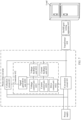
- FIG. 2 is a schematic of an application scenario of a photovoltaic inverter according to embodiments of this application.
- the power supply system includes a photovoltaic inverter 1, a power supply 2, and a load 3.
- the photovoltaic inverter 1 includes a conversion circuit 13, the power supply 2 may be connected to the load 3 through the conversion circuit 13, and an input of the photovoltaic inverter 1 may be separately connected to an input end and an output of the conversion circuit 13.
- the power supply 2 may supply power to the load 3 through the conversion circuit 13.
- the power supply 2 provided in this application is applicable to an application scenario in which the power supply 2 supplies power to a plurality of types of electrical devices, for example, supplies power to a base station device in a remote area with no mains electricity or poor mains electricity, or supplies power to a household device (such as a refrigerator or an air conditioner). This may be specifically determined based on an actual application scenario, and is not limited herein. It may be further understood that the load 3 in FIG. 2 may include a power grid, and the power grid herein may include an electrical device or a power transmission device such as a transmission line, a power transfer station, a communication base station, or a household device.
- the load 3 herein may further include a load (an electric apparatus or a power transmission apparatus) whose voltage and current are in a non-linear relationship in a running (power supply or power consumption) process, such as a motor or a rectifier device.
- the conversion circuit 13 may be an NPC inverter circuit. Refer to FIG. 1 . As shown in FIG. 1 , the conversion circuit 13 may include two groups of capacitors (for example, C11 and C12) and at least one switching bridge arm (for example, a switching bridge arm including switching transistors Ta1, Ta2, Ta3, and Ta4, a switching bridge arm including switching transistors Tb1, Tb2, Tb3, and Tb4, and a switching bridge arm including switching transistors Tc1, Tc2, Tc3, and Tc4).
- an output voltage (or an output current) of the photovoltaic inverter 1 is asymmetric (for example, different switching transistor models, different losses, asymmetric loads, or affected by factors such as a switching deadband), in a power supply cycle, a quantity of charges flowing into a neutral point of the conversion circuit 13 and a quantity of charges flowing out of the neutral point of the conversion circuit 13 are different. In other words, amounts of charged energy (or amounts of discharged energy) of the two groups of capacitors in the conversion circuit 13 are not equal.
- the photovoltaic inverter 1 may further include a collection circuit 11 and a controller 12.
- the collection circuit 11 may obtain the positive direct current bus voltage and the negative direct current bus voltage of the conversion circuit 13.
- the controller 12 may generate an even-order harmonic voltage regulation signal based on the positive direct current bus voltage and the negative direct current bus voltage of the conversion circuit 13 and a phase of the output voltage of the photovoltaic inverter 1, generate a drive control signal (for example, a drive control signal such as a PWM wave) based on the even-order harmonic voltage regulation signal, and control a switching transistor in the conversion circuit to be turned on or off.
- the photovoltaic inverter 1 may reduce a difference between the positive direct current bus voltage and the negative direct current bus voltage of the conversion circuit 13, to improve stability of the voltage at the neutral point of the conversion circuit 13. In this way, a structure is simple, a control method is easy, and applicability is high.
- the even-order harmonic component in the output current may interact with a fundamental component in the drive control signal, and/or an even-order harmonic component in the drive control signal may interact with a fundamental component in the output current, to adjust the potential of the neutral point of the conversion circuit 103, and balance the potential of the neutral point of the conversion circuit 103.
- even-order harmonic voltage regulation signal herein may be an even-order harmonic voltage regulation signal generated based on one type of even-order harmonic (for example, a second-order harmonic), or may be an even-order harmonic voltage regulation signal generated by superimposing a plurality of types of even-order harmonics (for example, a second-order harmonic and a fourth-order harmonic).
- the photovoltaic inverter may determine an amplitude of the even-order harmonic voltage regulation signal based on the positive direct current bus voltage and the negative direct current bus voltage of the conversion circuit, determine a phase of the even-order harmonic voltage regulation signal based on the phase of the output voltage of the photovoltaic inverter, and further generate the drive control signal based on the even-order harmonic voltage regulation signal.
- the photovoltaic inverter reduces the difference between the positive direct current bus voltage and the negative direct current bus voltage of the conversion circuit while controlling the conversion circuit to output the target voltage, to improve the stability of the voltage at the neutral point of the conversion circuit. In this way, a structure is simple, a control method is accurate and easy, and applicability is high.
- the collection circuit 101 may be further configured to obtain the phase of the output voltage of the photovoltaic inverter and a phase of an output current of the photovoltaic inverter.
- the controller 102 may further determine a type of the load based on the phase of the output voltage of the photovoltaic inverter and the phase of the output current of the photovoltaic inverter, and generate the even-order harmonic phase signal based on the phase of the output voltage of the photovoltaic inverter and the type of the load.
- the type of the load is one or more of an inductive load, a capacitive load, and/or a resistive load.
- the photovoltaic inverter may obtain the phase of the output voltage of the photovoltaic inverter and the phase of the output current of the photovoltaic inverter through the collection circuit 101, and further determine the type of the load based on the phase of the output voltage of the photovoltaic inverter and the phase of the output current of the photovoltaic inverter.
- different phases have different adjustment effects.
- the photovoltaic inverter may correspondingly generate a first phase for the resistive load, correspondingly generate a second phase for the capacitive load, and correspondingly generate a third phase for the inductive load.
- the photovoltaic inverter may generate a fourth phase for a plurality of types of mixed loads.
- the photovoltaic inverter may superimpose a first phase, a second phase, or a third phase for a plurality of types of mixed loads based on weights, to generate a new phase (for example, a fifth phase), and superimpose the first phase, the second phase, the third phase, the fourth phase, or the fifth phase with the phase that is of the output voltage of the photovoltaic inverter and based on which frequency multiplication is performed, to generate the even-order harmonic phase signal.
- the photovoltaic inverter herein may alternatively determine output power (including active power and reactive power) of the photovoltaic inverter based on the output voltage and the output current of the photovoltaic inverter, and determine the type of the load based on symbols of the active power and the reactive power of the photovoltaic inverter.
- the photovoltaic inverter may determine a power factor of the photovoltaic inverter based on the output voltage and the output current of the photovoltaic inverter, and determine the type of the load based on the power factor of the photovoltaic inverter. This may be specifically determined based on an application scenario.
- the photovoltaic inverter may generate the even-order harmonic voltage regulation signal based on the even-order harmonic amplitude signal and the even-order harmonic phase signal.
- the even-order harmonic voltage regulation signal herein may be an even-order harmonic voltage regulation signal generated based on one type of even-order harmonic (for example, a second-order harmonic), or may be an even-order harmonic voltage regulation signal generated by superimposing a plurality of types of even-order harmonics (for example, a second-order harmonic and a fourth-order harmonic).
- the photovoltaic inverter herein may generate a plurality of even-order harmonic phase signals with different phases for a plurality of types of mixed loads, generate a plurality of even-order harmonic voltage regulation signals based on the plurality of even-order harmonic phase signals with different phases and the even-order harmonic amplitude signal, and superimpose the plurality of even-order harmonic voltage regulation signals based on weights to obtain an even-order harmonic voltage regulation signal.
- the current control unit 5024 herein may be a current control loop, and the current feedback unit 5025 herein may obtain the output current of the photovoltaic inverter, and input the output current of the photovoltaic inverter to the current control unit 5024 as the current feedback signal; and further, the current control unit 5024 may adjust the level-1 voltage instruction signal output by the voltage control unit 5021 by comparing the level-1 voltage instruction signal with the current feedback signal, to generate the level-2 voltage instruction signal (that is, a voltage instruction signal adjusted based on the voltage feedback signal and the current feedback signal).
- the drive control unit 5022 may further generate the drive control signal based on the level-2 voltage instruction signal, and control, based on the drive control signal, a switching transistor in the conversion circuit 503 to be turned on or off.
- connection manners and working principles of a signal generation unit 6020, a voltage control unit 6021, a drive control unit 6022, a voltage feedback unit 6023, a current control unit 6024, and a current feedback unit 6025 that are in a controller 602 and a collection circuit 601 in FIG. 7 are the same as those of the signal generation unit 5020, the voltage control unit 5021, the drive control unit 5022, the voltage feedback unit 5023, the current control unit 5024, and the current feedback unit 5025 that are in the controller 502 and the collection circuit 501 in FIG. 6 . Details are not described herein again.
- the power supply system shown in FIG. 7 may further include a transformer 604, and the transformer 604 may be connected to a conversion circuit 603 and a load.
- the photovoltaic inverter, the power supply system, and functional modules in the power supply system have various and flexible composition manners, and can adapt to different power supply environments. Therefore, diversity of application scenarios of the power supply system is improved, and adaptability of the power supply system is enhanced.
- any power supply system or photovoltaic inverter shown in FIG. 1 to FIG. 7 may control turn-on or turn-off time of the switching transistor in the conversion circuit, to reduce the difference between the positive direct current bus voltage and the negative direct current bus voltage of the conversion circuit while controlling the conversion circuit to output the target voltage, thereby improving the stability of the voltage at the neutral point of the conversion circuit. In this way, a structure is simple, a control method is easy, and applicability is high.
- the following uses the structure of the power supply system shown in FIG. 2 as an example to describe on-grid control methods provided in embodiments of this application.
- FIG. 8 is a schematic flowchart of a control method according to this application.
- the control method provided in this application is applicable to a photovoltaic inverter.
- the photovoltaic inverter includes a conversion circuit and positive and negative direct current buses. One end of the positive and negative direct current buses is connected to the conversion circuit, and the other end of the positive and negative direct current buses is configured to connect to a power supply.
- the control method is also applicable to any one of the power supply systems shown in FIG. 1 to FIG. 7 or the photovoltaic inverters in the power supply systems. As shown in FIG. 8 , the control method provided in this application includes the following steps:
- the photovoltaic inverter may generate the even-order harmonic voltage regulation signal based on the positive direct current bus voltage and the negative direct current bus voltage of the conversion circuit and the phase of the output voltage of the photovoltaic inverter. Further, the photovoltaic inverter may generate a drive control signal based on the even-order harmonic voltage regulation signal, and control, based on the drive control signal, the switching transistor in the conversion circuit to be turned on or off.
- the photovoltaic inverter can reduce the difference between the positive direct current bus voltage and the negative direct current bus voltage of the conversion circuit while controlling the conversion circuit to output the target voltage, to improve stability of a voltage at a neutral point of the conversion circuit.
- a structure is simple, a control method is easy, and applicability is high.
- FIG. 9 is another schematic flowchart of a control method according to this application.
- step S701 in which the even-order harmonic voltage regulation signal is generated based on the positive direct current bus voltage of the conversion circuit, the negative direct current bus voltage of the conversion circuit, and the phase of the output voltage of the photovoltaic inverter may include the following steps:
- the photovoltaic inverter may generate the even-order harmonic voltage regulation signal based on the even-order harmonic amplitude signal and the even-order harmonic phase signal, further generate the drive control signal (for example, a drive control signal such as a PWM wave) based on the even-order harmonic voltage regulation signal, and control, based on the drive control signal, the switching transistor in the conversion circuit to be turned on or off.
- the drive control signal for example, a drive control signal such as a PWM wave
- the photovoltaic inverter may determine an amplitude of the even-order harmonic voltage regulation signal based on the positive direct current bus voltage and the negative direct current bus voltage of the conversion circuit, determine a phase of the even-order harmonic voltage regulation signal based on the phase of the output voltage of the photovoltaic inverter, and further generate the drive control signal based on the even-order harmonic voltage regulation signal.
- the photovoltaic inverter reduces the difference between the positive direct current bus voltage and the negative direct current bus voltage of the conversion circuit while controlling the conversion circuit to output the target voltage, to improve the stability of the voltage at the neutral point of the conversion circuit. In this way, a structure is simple, a control method is accurate and easy, and applicability is high.
- step S802 in which the even-order harmonic phase signal is generated based on the phase of the output voltage of the photovoltaic inverter may include: detecting the phase of the output voltage of the photovoltaic inverter and a phase of an output current of the photovoltaic inverter; and determining a type of a load based on the phase of the output voltage of the photovoltaic inverter and the phase of the output current of the photovoltaic inverter, and generating the even-order harmonic phase signal based on the phase of the output voltage of the photovoltaic inverter and the type of the load, where the type of the load is one or more of an inductive load, a capacitive load, and/or a resistive load.
- the photovoltaic inverter may detect the phase of the output voltage of the photovoltaic inverter and the phase of the output current of the photovoltaic inverter through the collection circuit, and further determine the type of the load based on the phase of the output voltage of the photovoltaic inverter and the phase of the output current of the photovoltaic inverter.
- different phases have different adjustment effects.
- the photovoltaic inverter may correspondingly generate a first phase for the resistive load, correspondingly generate a second phase for the capacitive load, and correspondingly generate a third phase for the inductive load.
- the photovoltaic inverter may generate a fourth phase for a plurality of types of mixed loads.
- the photovoltaic inverter may superimpose a first phase, a second phase, or a third phase for a plurality of types of mixed loads based on weights, to generate a new phase (for example, a fifth phase), and superimpose the first phase, the second phase, the third phase, the fourth phase, or the fifth phase with the phase that is of the output voltage of the photovoltaic inverter and based on which frequency multiplication is performed, to generate the even-order harmonic phase signal.
- the photovoltaic inverter herein may alternatively determine output power (including active power and reactive power) of the photovoltaic inverter based on the output voltage and the output current of the photovoltaic inverter, and determine the type of the load based on symbols of the active power and the reactive power of the conversion circuit.
- the photovoltaic inverter may determine a power factor of the conversion circuit based on the output voltage and the output current of the photovoltaic inverter, and determine the type of the load based on the power factor of the conversion circuit. This may be specifically determined based on an application scenario.
- the photovoltaic inverter may generate the even-order harmonic voltage regulation signal based on the even-order harmonic amplitude signal and the even-order harmonic phase signal.
- the even-order harmonic voltage regulation signal herein may be an even-order harmonic voltage regulation signal generated based on one type of even-order harmonic (for example, a second-order harmonic), or may be an even-order harmonic voltage regulation signal generated by superimposing a plurality of types of even-order harmonics (for example, a second-order harmonic and a fourth-order harmonic).
- the photovoltaic inverter may determine the type of the load based on the phase of the output voltage and the phase of the output current of the photovoltaic inverter, determine the phase of the even-order harmonic voltage regulation signal based on the phase of the output voltage of the photovoltaic inverter and the type of the load, and then generate the drive control signal based on the even-order harmonic voltage regulation signal.
- the photovoltaic inverter may generate targeted drive control signals based on different types of loads, to reduce the difference between the positive direct current bus voltage and the negative direct current bus voltage of the conversion circuit while controlling the conversion circuit to output the target voltage, thereby improving the stability of the voltage at the neutral point of the conversion circuit. In this way, a structure is simple, a control method is easy, applicability is high, and control efficiency is high.
- step S702 in which the voltage instruction signal of the conversion circuit is generated based on the even-order harmonic voltage regulation signal may include: detecting a fundamental wave instruction of an external central control system; and superposing the fundamental wave instruction and the even-order harmonic voltage regulation signal to obtain the voltage instruction signal of the conversion circuit.
- the photovoltaic inverter herein may detect the fundamental wave instruction sent by the external central control system, directly obtain a fundamental wave signal based on the fundamental wave instruction or obtain a fundamental wave signal through calculation, and superpose and modulate the fundamental wave signal and the even-order harmonic voltage regulation signal, to obtain the voltage instruction signal of the conversion circuit; and further, the photovoltaic inverter may generate the drive control signal based on the voltage instruction signal, and control, based on the drive control signal, the switching transistor in the conversion circuit to be turned on or off. In this way, a structure is simple, a control method is easy, and control efficiency is high.
- the method may further include: detecting the output voltage of the photovoltaic inverter, and using the output voltage of the photovoltaic inverter as a voltage feedback signal; generating a level-1 voltage instruction signal based on the voltage feedback signal and the voltage instruction signal of the conversion circuit; and generating the drive control signal based on the level-1 voltage instruction signal.
- the photovoltaic inverter herein may detect the output voltage of the photovoltaic inverter, and use the output voltage of the photovoltaic inverter as the voltage feedback signal, so that the photovoltaic inverter may adjust the voltage instruction signal by comparing the voltage instruction signal with the voltage feedback signal, and generate the level-1 voltage instruction signal (that is, a voltage instruction signal adjusted based on the voltage feedback signal). Further, the photovoltaic inverter may further generate the drive control signal based on the level-1 voltage instruction signal, and control, based on the drive control signal, the switching transistor in the conversion circuit to be turned on or off.
- the photovoltaic inverter may adjust the drive control signal in real time by using the output voltage of the photovoltaic inverter as the voltage feedback signal. Therefore, control efficiency is high.
- the method may further include: detecting the output current of the photovoltaic inverter, and using the output current of the photovoltaic inverter as a current feedback signal; generating a level-2 voltage instruction signal based on the level-1 voltage instruction signal and the current feedback signal; and generating the drive control signal based on the level-2 voltage instruction signal.
- the photovoltaic inverter herein may detect the output current of the photovoltaic inverter, and use the output current of the photovoltaic inverter as the current feedback signal, so that the photovoltaic inverter may adjust the level-1 voltage instruction signal by comparing the level-1 voltage instruction signal with the current feedback signal, and generate the level-2 voltage instruction signal (that is, a voltage instruction signal adjusted based on the voltage feedback signal and the current feedback signal).
- the photovoltaic inverter may further generate the drive control signal based on the level-2 voltage instruction signal, and control, based on the drive control signal, the switching transistor in the conversion circuit to be turned on or off.
- the photovoltaic inverter may adjust the drive control signal in real time by using the output current of the photovoltaic inverter as the current feedback signal. Therefore, control efficiency is high.
Landscapes
- Engineering & Computer Science (AREA)
- Power Engineering (AREA)
- Inverter Devices (AREA)
- Control Of Electrical Variables (AREA)
Applications Claiming Priority (2)
| Application Number | Priority Date | Filing Date | Title |
|---|---|---|---|
| CN202211131328.8A CN115498906A (zh) | 2022-09-16 | 2022-09-16 | 光伏逆变器及其控制方法 |
| PCT/CN2023/104301 WO2024055705A1 (fr) | 2022-09-16 | 2023-06-29 | Onduleur photovoltaïque et son procédé de commande |
Publications (2)
| Publication Number | Publication Date |
|---|---|
| EP4580030A1 true EP4580030A1 (fr) | 2025-07-02 |
| EP4580030A4 EP4580030A4 (fr) | 2025-11-26 |
Family
ID=84468250
Family Applications (1)
| Application Number | Title | Priority Date | Filing Date |
|---|---|---|---|
| EP23864443.9A Pending EP4580030A4 (fr) | 2022-09-16 | 2023-06-29 | Onduleur photovoltaïque et son procédé de commande |
Country Status (4)
| Country | Link |
|---|---|
| US (1) | US20250211132A1 (fr) |
| EP (1) | EP4580030A4 (fr) |
| CN (1) | CN115498906A (fr) |
| WO (1) | WO2024055705A1 (fr) |
Families Citing this family (2)
| Publication number | Priority date | Publication date | Assignee | Title |
|---|---|---|---|---|
| CN115498906A (zh) * | 2022-09-16 | 2022-12-20 | 华为数字能源技术有限公司 | 光伏逆变器及其控制方法 |
| CN116388591A (zh) * | 2023-03-06 | 2023-07-04 | 华为数字能源技术有限公司 | 一种逆变器和逆变器控制方法 |
Family Cites Families (9)
| Publication number | Priority date | Publication date | Assignee | Title |
|---|---|---|---|---|
| JPH09182455A (ja) * | 1995-12-21 | 1997-07-11 | Fuji Electric Co Ltd | 3レベルインバータの制御回路 |
| JP5952087B2 (ja) * | 2012-05-24 | 2016-07-13 | 株式会社日立製作所 | 電力変換装置 |
| JP2013255317A (ja) * | 2012-06-06 | 2013-12-19 | Meidensha Corp | 3レベルインバータの制御装置 |
| CN105226982B (zh) * | 2015-11-02 | 2018-01-12 | 南京航空航天大学 | 一种基于中点电流的三电平npc逆变器中点电位均衡控制方法 |
| CN106099971B (zh) * | 2016-05-18 | 2018-08-07 | 艾思玛新能源技术(江苏)有限公司 | 提高单相光伏逆变器对弱电网的适应性的控制方法及系统 |
| CN108631326A (zh) * | 2018-04-26 | 2018-10-09 | 南京理工大学 | 基于Buck型三电平交交变换器的无功和谐波补偿装置 |
| CN114982121B (zh) * | 2020-09-08 | 2023-10-13 | 华为数字能源技术有限公司 | 一种三电平逆变器、控制方法及系统 |
| JP7316259B2 (ja) * | 2020-10-05 | 2023-07-27 | 東芝三菱電機産業システム株式会社 | 3レベル電力変換器の制御装置 |
| CN115498906A (zh) * | 2022-09-16 | 2022-12-20 | 华为数字能源技术有限公司 | 光伏逆变器及其控制方法 |
-
2022
- 2022-09-16 CN CN202211131328.8A patent/CN115498906A/zh active Pending
-
2023
- 2023-06-29 EP EP23864443.9A patent/EP4580030A4/fr active Pending
- 2023-06-29 WO PCT/CN2023/104301 patent/WO2024055705A1/fr not_active Ceased
-
2025
- 2025-03-14 US US19/080,485 patent/US20250211132A1/en active Pending
Also Published As
| Publication number | Publication date |
|---|---|
| WO2024055705A1 (fr) | 2024-03-21 |
| US20250211132A1 (en) | 2025-06-26 |
| CN115498906A (zh) | 2022-12-20 |
| EP4580030A4 (fr) | 2025-11-26 |
Similar Documents
| Publication | Publication Date | Title |
|---|---|---|
| US9923484B2 (en) | Method and system for operating a multilevel electric power inverter | |
| EP4432545A1 (fr) | Onduleur et son procédé de commande | |
| EP2357721B1 (fr) | Dispositif de conversion de courant | |
| CN102856916B (zh) | 一种单相光伏逆变器无功控制方法及电路 | |
| US20250211132A1 (en) | Photovoltaic Inverter and Control Method Thereof | |
| AU2012297567C1 (en) | Power conversion system | |
| US10193434B2 (en) | Power conversion device and three-phase AC power supply device | |
| CN104539182B (zh) | 一种带有自平衡辅助桥臂的五电平中点钳位逆变器拓扑 | |
| US11228258B2 (en) | Uninterruptible power supply apparatus | |
| KR20150003796A (ko) | 다수의 dc 소스를 갖는 양방향 에너지 컨버터 | |
| CN103023070A (zh) | 基于3d-spwm的混合箝位式三电平三相四线制光伏系统 | |
| Yibre et al. | Supercapacitors for wind power application | |
| Kumar et al. | Asymmetrical three-phase multilevel inverter for grid-integrated PLL-less system | |
| CN115241926A (zh) | 母线电压控制方法、母线平衡控制方法及其系统 | |
| Kankanala et al. | Modeling and control of cascaded bridgeless multilevel rectifier under unbalanced load conditions | |
| Zhu et al. | Grid synchronization control without AC voltage sensors | |
| CN104124884A (zh) | 光伏逆变器和光伏空调系统 | |
| Liu et al. | Pulse width amplitude modulation based single-phase quasi-Z-source photovoltaic inverter with energy storage battery | |
| Li et al. | Dual buck based power decoupling circuit for single phase inverter/rectifier | |
| Hui et al. | A novel active power filter using multilevel converter with self voltage balancing | |
| CN104979822A (zh) | 智能微电网电力质量管理的操作系统 | |
| Zhang et al. | Modal Analysis of Photovoltaic Power Supply Circuit for Boost-Type Three-Port Converter | |
| Wang | Research on dual-terminal flexible HVDC transmission system based on renewable energy access | |
| Bhat et al. | A generalized space vector modulation with simple control technique for balancing DC-bus capacitor voltages of a three-phase, neutral-point clamped converter | |
| Zhang et al. | The Modulation and Control Strategy of DC-link Current Minimization for Single-Phase Current Source Inverter |
Legal Events
| Date | Code | Title | Description |
|---|---|---|---|
| STAA | Information on the status of an ep patent application or granted ep patent |
Free format text: STATUS: THE INTERNATIONAL PUBLICATION HAS BEEN MADE |
|
| PUAI | Public reference made under article 153(3) epc to a published international application that has entered the european phase |
Free format text: ORIGINAL CODE: 0009012 |
|
| STAA | Information on the status of an ep patent application or granted ep patent |
Free format text: STATUS: REQUEST FOR EXAMINATION WAS MADE |
|
| 17P | Request for examination filed |
Effective date: 20250325 |
|
| AK | Designated contracting states |
Kind code of ref document: A1 Designated state(s): AL AT BE BG CH CY CZ DE DK EE ES FI FR GB GR HR HU IE IS IT LI LT LU LV MC ME MK MT NL NO PL PT RO RS SE SI SK SM TR |
|
| REG | Reference to a national code |
Ref country code: DE Ref legal event code: R079 Free format text: PREVIOUS MAIN CLASS: H02M0007480000 Ipc: H02M0007487000 |
|
| A4 | Supplementary search report drawn up and despatched |
Effective date: 20251027 |
|
| RIC1 | Information provided on ipc code assigned before grant |
Ipc: H02M 7/487 20070101AFI20251021BHEP Ipc: H02M 7/5387 20070101ALI20251021BHEP Ipc: H02M 1/00 20060101ALI20251021BHEP Ipc: H02M 1/12 20060101ALI20251021BHEP Ipc: H02M 7/483 20070101ALI20251021BHEP |
|
| DAV | Request for validation of the european patent (deleted) | ||
| DAX | Request for extension of the european patent (deleted) |