EP4580039A1 - Appareil de commande d'entraînement et procédé de commande d'entraînement pour machine électrique tournante - Google Patents
Appareil de commande d'entraînement et procédé de commande d'entraînement pour machine électrique tournante Download PDFInfo
- Publication number
- EP4580039A1 EP4580039A1 EP23857058.4A EP23857058A EP4580039A1 EP 4580039 A1 EP4580039 A1 EP 4580039A1 EP 23857058 A EP23857058 A EP 23857058A EP 4580039 A1 EP4580039 A1 EP 4580039A1
- Authority
- EP
- European Patent Office
- Prior art keywords
- modulation wave
- phase
- modulation
- value
- wave
- Prior art date
- Legal status (The legal status is an assumption and is not a legal conclusion. Google has not performed a legal analysis and makes no representation as to the accuracy of the status listed.)
- Pending
Links
Images







Classifications
-
- H—ELECTRICITY
- H02—GENERATION; CONVERSION OR DISTRIBUTION OF ELECTRIC POWER
- H02M—APPARATUS FOR CONVERSION BETWEEN AC AND AC, BETWEEN AC AND DC, OR BETWEEN DC AND DC, AND FOR USE WITH MAINS OR SIMILAR POWER SUPPLY SYSTEMS; CONVERSION OF DC OR AC INPUT POWER INTO SURGE OUTPUT POWER; CONTROL OR REGULATION THEREOF
- H02M7/00—Conversion of AC power input into DC power output; Conversion of DC power input into AC power output
- H02M7/42—Conversion of DC power input into AC power output without possibility of reversal
- H02M7/44—Conversion of DC power input into AC power output without possibility of reversal by static converters
- H02M7/48—Conversion of DC power input into AC power output without possibility of reversal by static converters using discharge tubes with control electrode or semiconductor devices with control electrode
- H02M7/53—Conversion of DC power input into AC power output without possibility of reversal by static converters using discharge tubes with control electrode or semiconductor devices with control electrode using devices of a triode or transistor type requiring continuous application of a control signal
- H02M7/537—Conversion of DC power input into AC power output without possibility of reversal by static converters using discharge tubes with control electrode or semiconductor devices with control electrode using devices of a triode or transistor type requiring continuous application of a control signal using semiconductor devices only, e.g. single switched pulse inverters
- H02M7/5387—Conversion of DC power input into AC power output without possibility of reversal by static converters using discharge tubes with control electrode or semiconductor devices with control electrode using devices of a triode or transistor type requiring continuous application of a control signal using semiconductor devices only, e.g. single switched pulse inverters in a bridge configuration
-
- H—ELECTRICITY
- H02—GENERATION; CONVERSION OR DISTRIBUTION OF ELECTRIC POWER
- H02M—APPARATUS FOR CONVERSION BETWEEN AC AND AC, BETWEEN AC AND DC, OR BETWEEN DC AND DC, AND FOR USE WITH MAINS OR SIMILAR POWER SUPPLY SYSTEMS; CONVERSION OF DC OR AC INPUT POWER INTO SURGE OUTPUT POWER; CONTROL OR REGULATION THEREOF
- H02M1/00—Details of apparatus for conversion
- H02M1/12—Arrangements for reducing harmonics from AC input or output
-
- H—ELECTRICITY
- H02—GENERATION; CONVERSION OR DISTRIBUTION OF ELECTRIC POWER
- H02P—CONTROL OR REGULATION OF ELECTRIC MOTORS, ELECTRIC GENERATORS OR DYNAMO-ELECTRIC CONVERTERS; CONTROLLING TRANSFORMERS, REACTORS OR CHOKE COILS
- H02P27/00—Arrangements or methods for the control of AC motors characterised by the kind of supply voltage
- H02P27/04—Arrangements or methods for the control of AC motors characterised by the kind of supply voltage using variable-frequency supply voltage, e.g. inverter or converter supply voltage
- H02P27/06—Arrangements or methods for the control of AC motors characterised by the kind of supply voltage using variable-frequency supply voltage, e.g. inverter or converter supply voltage using DC to AC converters or inverters
- H02P27/08—Arrangements or methods for the control of AC motors characterised by the kind of supply voltage using variable-frequency supply voltage, e.g. inverter or converter supply voltage using DC to AC converters or inverters with pulse width modulation
- H02P27/085—Arrangements or methods for the control of AC motors characterised by the kind of supply voltage using variable-frequency supply voltage, e.g. inverter or converter supply voltage using DC to AC converters or inverters with pulse width modulation wherein the PWM mode is adapted on the running conditions of the motor, e.g. the switching frequency
Definitions
- an inverter that converts DC power into AC power is used as a power converter for variable-speed driving of a rotating electrical machine.
- a semiconductor element performs a switching operation by pulse width modulation (PWM) control to convert a DC voltage into an AC voltage having any frequency and any amplitude.
- PWM pulse width modulation
- a PWM pulse mode having a higher modulation rate and a higher switching frequency is more likely to have a narrower pulse width, and this problem is more likely to appear.
- a voltage error has occurred, there is a problem that a torque error of the rotating electrical machine, an increase in current ripple, and the like are caused.
- PTL 1 discloses a technology of performing control in accordance with a voltage command value obtained by adding 1/2 of an intermediate value of instantaneous voltage command values of phases to the instantaneous voltage command values of the phases for the purpose of reducing the harmonic current and improving a voltage utilization rate.
- PTL 2 discloses a technology as follows.
- a pulse width error caused by pulse width limitation of a phase voltage signal is calculated by an error in a line-to-line voltage pulse width, and the error in the line-to-line voltage pulse width is corrected by a pulse width of a phase voltage signal of a phase other than a phase in which the pulse width is limited.
- an error in the line-to-line voltage pulse width due to the pulse width correction of the phase voltage signal is corrected by the pulse width of the phase voltage signal of a phase other than the two phases of the phase in which the minimum pulse width limitation has been performed, and the phase in which the pulse width correction has been performed.
- the inventors of the present application have extensively conducted studies for the purpose of outputting an accurate fundamental wave voltage while reducing a harmonic current by PWM control, and as a result, have obtained the following findings.
- the technology disclosed in PTL 1 discloses a technology for reducing a harmonic current by adding an operation amount of a modulation wave including a third harmonic component (a voltage waveform of a frequency component of three times a fundamental wave voltage) to a modulation wave of a three-phase sine wave to distort the modulation wave.
- a third harmonic component a voltage waveform of a frequency component of three times a fundamental wave voltage
- the present invention has been made in view of the above points, and on the basis of the technology disclosed in PTL 1, even in an overmodulation region in which a modulation wave is made higher than a carrier wave and some of PWM pulses are eliminated, a voltage error due to limitation of a minimum pulse width is suppressed while reducing a harmonic current, and an accurate voltage is output.
- An object of the present invention is to provide a PWM control technology for outputting an accurate fundamental wave voltage while reducing a harmonic current by adding an operation amount to modulation waves of three phases in accordance with saturation states of the modulation waves of the three phases.
- one of typical drive control apparatuses for a rotating electrical machine is a drive control apparatus that drives the rotating electrical machine by controlling an electric power conversion device by a PWM signal generated by a PWM control unit from three-phase modulation wave command values generated on the basis of a voltage command value and a carrier wave.
- the drive control apparatus includes a modulation wave operation unit provided at a preceding stage of the PWM control unit.
- the modulation wave operation unit adds an operation amount to the modulation wave command value of one phase to be saturated up to a maximum value of an absolute value of the carrier wave and to stop switching of the one phase in the electric power conversion device, and adds the operation amount to modulation wave command values of the remaining two phases, when an absolute value of a modulation wave command value of the one phase among the three-phase modulation wave command values is greater than a prescribed value, and adds the operation amount to the modulation wave command values of the two phases to be saturated up to the maximum value of the absolute value of the carrier wave and to stop switching of the two phases in the electric power conversion device, when absolute values of the modulation wave command values of any two phase among the three-phase modulation wave command values are greater than the prescribed value.
- the present invention for example, in an overmodulation region, it is possible to output an accurate voltage while reducing a harmonic current, and it is possible to realize efficiency improvement and stable control of a drive system.
- constituent elements having the same reference signs are indicated as constituent elements having the same or similar functions.
- description of the same or similar constituent elements as those in the embodiments described above may be omitted.
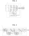
- FIG. 2 is a view illustrating an example of a drive apparatus for a rotating electrical machine to which a PWM control method according to Embodiment 1 is applied.
- the drive apparatus includes a rotating electrical machine 4 to be controlled, a drive device 1 that drives the rotating electrical machine 4, a main circuit unit 3 that applies a three-phase AC voltage to the rotating electrical machine 4, a gate drive 6 that outputs a gate signal for driving the main circuit unit 3, a control apparatus 2 that outputs a PWM signal to the gate drive 6, and a current detector 5 that detects a current flowing through the rotating electrical machine 4 by the control apparatus 2.
- the gate drive 6 outputs a gate signal on the basis of the PWM signal.
- the current detector 5 includes a hole current transformer (CT) or the like, and detects waveforms of three-phase currents i u , i v , and i w of a U-phase, a V-phase, and a W-phase flowing through the rotating electrical machine 4.
- CT hole current transformer
- the current detector 5 does not necessarily need to detect all the currents of the three phases, and the current detector 5 may be configured to detect any two phases of the three phases and obtain the remaining one phase by calculation assuming that the three-phase currents are in an equilibrium state.
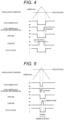
- FIG. 3 illustrates an example of functional blocks of the control apparatus according to Embodiment 1. Here, only the minimum necessary functional blocks for Embodiment 1 are illustrated.
- a modulation wave command calculation unit 10 calculates a voltage command value by vector control (not illustrated) or the like on the basis of the three-phase currents i u , i v , and i w detected by the current detector 5, and outputs three-phase modulation wave command values a uo *, a v0 *, and a w0 * on the basis of the voltage command value.
- a current control unit, a frequency calculation unit, a phase calculation unit, a voltage vector calculation unit, and the like used for general vector control are collectively referred to as a modulation wave command calculation unit 10 for simplification of description.
- a PWM control unit 13 receives inputs of the three-phase modulation wave command values a u *, a v *, and a w * corrected by a zero-phase modulation wave calculation unit 11 and a modulation wave error correction unit 12, compares the magnitude with a carrier wave of a triangular wave, and performs pulse width modulation.
- a PWM signal subjected to the pulse width modulation is output to the gate drive 6 ( FIG. 2 ).
- the PWM control unit 13 includes means for limiting a pulse width such as a dead time period or a minimum ON-time in order to prevent a failure of a switching element constituting the main circuit unit 3.
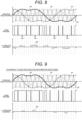
- FIG. 4 illustrates a relationship between a pulse command value and an output voltage when a pulse width of the pulse command value is sufficiently wide.
- the pulse command value is calculated in consideration of a dead time period T off , and the final output voltage coincides with the pulse command value.
- T off a dead time period
- the potential is determined by the polarity of the current. Therefore, in FIG. 4 , the current polarity during the dead time period is assumed to be positive, and the potential during the dead time period is set to zero (mark on "output voltage" at the bottom of FIG. 4 ).
- FIG. 5 illustrates a relationship between a pulse command value and an output voltage when a pulse command value in which a pulse width of the pulse command value is equal to or less than a set minimum pulse width is output.
- the output pulse width is limited to the set minimum pulse width, and the actual output voltage has an error with respect to the pulse command value.
- the voltage error is likely to occur under a condition that three-phase modulation waves cross near the peak points of the peak and valley of the carrier wave, that is, in a PWM pulse mode in which the frequency of the carrier wave is high and the modulation rate is high.
- the zero-phase modulation wave calculation unit 11 and the modulation wave error correction unit 12 illustrated in FIG. 3 reduce the harmonic current and suppress the voltage error by limiting the minimum pulse width for reducing distortion.
- the zero-phase modulation wave calculation unit 11 illustrated in FIG. 3 calculates and outputs a zero-phase modulation wave correction amount a mod_0 * from the three-phase modulation wave command values a u0 *, a v0 *, and a w0 * in order to improve the voltage utilization rate and reduce the harmonic current.
- FIG. 6 is a view illustrating an example of a calculation method of the zero-phase modulation wave calculation unit 11.
- FIG. 7 illustrates a description of a waveform when the zero-phase voltage is added.
- FIG. 6 illustrates a method of adding an average value of the maximum value and the minimum value of the three-phase voltage command values to all the modulation waves of the three phases as a zero-phase modulation wave correction amount a mod_0 *, as disclosed in PTL 1, as one of preferable forms of the zero-phase modulation wave calculation.
- the corrected three-phase modulation waves become waveforms 300 to 302 in which the peak of the peak value of the modulation wave is suppressed with respect to the time of sine wave modulation, and can be output at a higher voltage utilization rate.
- the range of the modulation rate that can be used without overmodulation can be used up to about 79% in the three-phase modulation waves (before correction) 200 to 202 as in (Math. 1).
- the zero-phase modulation wave correction amount a mod_0 * when added, it is ideally possible to use the range up to about 91%, but the pulse width is narrowed at a portion indicated as 500 of a U-phase PWM signal illustrated in FIG. 7 .
- the modulation rate by increasing the modulation rate, a value that is equal to or less than the minimum pulse width described with reference to FIG. 5 is obtained, and thus, it is not possible to actually use the range up to 91%.
- Embodiment 1 in the case of outputting a pulse narrower than the minimum pulse width with respect to the restriction of the minimum pulse width, the operation amount is added to the modulation wave in advance to eliminate the pulse, thereby preventing the occurrence of the voltage error.
- FIG. 8 illustrates a waveform when the pulse is eliminated in advance by adding the operation amount to the modulation wave with respect to the waveform illustrated in FIG. 7 .
- an operation amount is added to the three-phase modulation waves in order to eliminate the pulse, and the absolute value of the modulation wave is made greater than that of the carrier wave only at this portion.
- the amplitude of the modulation wave is increased by adding the operation amount at the portion where the pulse becomes narrower than the minimum pulse width, so that an error occurs in a direction in which the finally output voltage becomes larger than the original command value (a u0 **, a v0 ** , and a w0 ** illustrated in FIG. 3 ).
- FIG. 9 is a view illustrating a waveform in a case where the operation amount is added to the modulation wave of another phase when the pulse is eliminated in advance by adding the operation amount to the modulation wave. That is, regarding the modulation wave ( FIG. 8 ) in which the pulse is eliminated by adding the operation amount to the modulation wave obtained by adding the zero-phase modulation wave correction amount ( FIG. 7 ), the operation amount is added to the modulation waves of other phases. That is, in a period in which the pulse is eliminated by adding the operation amount to the modulation wave of only one phase, the same amount as the operation amount is also added to the modulation waves of the remaining two phases.
- the common operation amount a mod_u * is also added to the remaining V-phase and W-phase modulation waves.
- the phase voltage of the rotating electrical machine 4 changes as shown in (Math. 3), but as shown in (Math. 4) and (Math. 5), the phase voltage does not influence the line-to-line voltage (here, between U and V) applied to the rotating electrical machine 4 before and after the operation amount a mod_u * is applied.
- the voltage applied to the rotating electrical machine 4 does not change as long as the line-to-line voltage applied to the rotating electrical machine 4 does not change.
- FIG. 10 is a flowchart illustrating an example of compensation amount calculation by the modulation wave error correction unit 12.
- saturation of a modulation wave of one phase or saturation of modulation waves of two or more phases is determined from comparison between the command value of the pulse width of each phase and the set minimum pulse width, and a mod_w * is calculated from the operation amount a mod_u * of each of the U-phase to the W-phase.
- FIG. 10 illustrates only a flowchart for calculating a compensation amount a mod_u * of the U-phase, and does not illustrate the V-phase and the W-phase, but the compensation amount is calculated in a similar flow also in the V-phase and the W-phase.
- the phase relationship between the modulation wave and the carrier wave is synchronized.
- the phase in which the pulse width is first narrower than the minimum pulse width is always the same (when viewed in FIG. 7 , a portion indicated as 500 of the U-phase PWM signal), and the number of phases saturated in each phase (only one phase, two or more phases, or the like) is also naturally determined.
- the modulation wave error correction unit 12 in the synchronous PWM may be configured to determine the compensation amount of each phase from the relationship between the voltage phase and the modulation rate without sequentially comparing the saturation states of the phases.
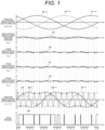
- FIG. 1 is a view illustrating an example of the relationship between the modulation wave and the carrier wave, and the PWM voltage waveform according to the present invention.
- the zero-phase modulation wave correction amount a mod_0 * 210 (the second stage in FIG. 1 ) calculated by the zero-phase modulation wave calculation unit 11 is added to the three-phase modulation waves 200 to 202 (the uppermost stage in FIG. 1 ) of the sine wave before correction.
- the pulse is eliminated by adding the operation amounts 220 to 222 (the third to fifth stages in FIG. 1 ) to the modulation wave (the period indicated as A and B in the lowermost stage in FIG. 1 ).
- the same amount as the operation amount is also added to the modulation waves of the remaining two phases (the period indicated as A in the lowermost stage of FIG. 1 ).
- the period B in the lowermost stage of FIG. 1 indicates a period in which the absolute value of the modulation wave of two or more phases is greater than the prescribed value.
- the corrected three-phase modulation waves 300 to 302 can be obtained.
- FIG. 12 illustrates a waveform in which the pulse base (peak-valley cycle) of the carrier wave is 15 cycles (15PB) in one cycle of the voltage waveform and the PWM voltage waveform has a waveform of synchronous 7 pulses.
- FIG. 13 illustrates a waveform before elimination of the pulse of the synchronous 21 pulses in the PWM voltage waveform, in which the pulse base (peak/valley cycle) of the carrier wave is 21 cycles (21PB) in one cycle of the voltage waveform.
- FIG. 14 illustrates a waveform in which the pulse base (peak/valley cycle) of the carrier wave is 21 cycles (21PB) in one cycle of the voltage waveform, and the pulse is eliminated to change the PWM voltage waveform from a state of the synchronous 21 pulses to the synchronous 17 pulses.
- FIG. 15 illustrates a waveform in which the pulse base (peak/valley cycle) of the carrier wave is 21 cycles (21PB) in one cycle of the voltage waveform, the pulse is further eliminated from FIG. 14 to change the PWM voltage waveform from a state of synchronous 17 pulses to synchronous 13 pulses (synchronous 13 pulses A).
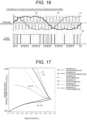
- FIG. 16 illustrates a waveform in a case of a modification example (synchronous 13 pulses B) of the synchronous 13 pulses illustrated in FIG. 15 .
- a period C in a period in which the absolute values of modulation waves of two phases become greater than a prescribed value, an operation amount is added to the remaining one phase. That is, the period C is a period in which the absolute values of the modulation waves of two or more phases become greater than the prescribed value and the operation amount is applied to the remaining one phase.
- a period B of FIG. 14 is a period in which the absolute values of the modulation waves of two or more phases become greater than the prescribed value, but the operation amount is not applied to the remaining one phase.
- the absolute values of the modulation waves of two or more phases are greater than the prescribed value in any period, and thus only the process of adding the operation amount to the modulation wave and stopping the switching is performed. This makes it possible to prevent the occurrence of a voltage error due to the minimum pulse width.
- the absolute values of the modulation waves of two or more phases are greater than the prescribed value in any period, and thus only the process of adding the operation amount to the modulation wave and stopping the switching is performed.
- Embodiment 2 The configuration in Embodiment 2 is different from Embodiment 1 in that a modulation wave amplitude correction unit 20 is added to the control apparatus 2.
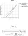
- FIG. 24 illustrates a relationship between a modulation rate (command value) and an actual modulation rate in synchronous 11 pulses in which the pulse base of the carrier wave is 15 cycles in one cycle of the voltage waveform.
- (j) and (i) of FIG. 24 are obtained by comparison of the modulation rate (fundamental wave voltage) in the presence or absence of modulation wave compensation to another phase described above in Embodiment 1, and it can be seen that the voltage output accuracy is improved in the case of "with compensation" of (j) (effect described in Embodiment 1).
- an actual modulation rate Am has an error with respect to a modulation rate (command value) Am* due to an influence of the U-V modulation wave error 600 illustrated in FIG. 9 .
- An amplitude correction coefficient calculation unit 21 receives inputs of the PWM mode and the modulation rate (command value) Am*, and outputs an amplitude correction coefficient. As illustrated in FIG. 24 , the relationship between the modulation rate (command value) Am* and the actual modulation rate Am can be defined in advance for each PWM mode. A correction coefficient for equalizing the relationship between the modulation rate (command value) and the actual modulation rate is derived. For the calculation of the correction coefficient, a configuration in which a function obtained by functionalizing the characteristics illustrated in FIGS. 24 and 26 is used, or table data illustrated in FIGS. 24 and 26 is directly used may be adopted.
- Embodiment 2 the synchronous PWM in which the carrier wave and the modulation wave are synchronized is used as the premise, and thus, the timing of eliminating the pulse and the influence of an elimination operation on the voltage error are uniquely determined.
- the influence of the U-V modulation wave error 600 illustrated in FIG. 9 cannot be corrected at that moment, but can be corrected such that the modulation rate (command value) Am* coincides with the actual modulation rate Am when viewed in the entire one cycle of the voltage waveform.
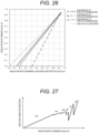
- FIG. 26 illustrates a relationship between the modulation rate (command value) and the actual modulation rate in another PWM mode.
- the relationship between the modulation rate (command value) Am* and the modulation rate Am varies depending on the PWM mode, and thus the correction coefficient is switched for each PWM mode.
- FIG. 27 illustrates a conceptual view of an output from the amplitude correction coefficient calculation unit 21 when the modulation rate increases.
- the amplitude correction coefficient having a different slope is output for each PWM mode in accordance with the PWM mode and the modulation rate (command value) Am*.
- the drive apparatus for a rotating electrical machine to which the PWM control method according to Embodiment 2 is applied corrects the modulation wave amplitude for each PWM mode by the modulation wave amplitude correction unit 20, whereby it is possible to correct a voltage error in a period in which a pulse is eliminated by adding an operation amount to modulation waves of two phases, and to output an accurate fundamental wave voltage.
- Embodiment 2 it is possible to reduce the occurrence of torque errors and current ripples as compared with Embodiment 1.
- Embodiment 3 is different from Embodiment 2 described above in that a PWM mode switching unit 22 is further added to the control apparatus 2.
- a contact line voltage greatly varies depending on a delivery voltage of a substation, a distance between the vehicle and the substation, and an operation state of another vehicle. Therefore, the modulation rate at the time of acceleration/deceleration also greatly changes. In addition, not only starting from the stop but also restarting from the coasting (free run) is required. Therefore, it is necessary to accurately output the voltage even at any frequency and modulation rate including the time when the contact line voltage varies.
- the limited range is also expanded as the switching frequency is increased at a high modulation rate (for example, in a case of driving in a high-speed range by multi-pulse synchronous PWM). Therefore, the range in which the voltage output with the minimum pulse width is possible also changes depending on the frequency in each PWM mode.
- FIG. 28 is a view illustrating an example of functional blocks of a control apparatus used in Embodiment 3.
- the PWM mode switching unit 22 receives inputs of the inverter frequency, the modulation rate, and the minimum pulse width, and outputs a PWM mode switching signal to the modulation wave amplitude correction unit 20 and the modulation wave error correction unit 12.
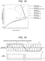
- FIG. 29 illustrates an example of an outline of functions by the PWM mode switching unit 22 added in Embodiment 3.
- the PWM mode range to be used is defined in accordance with the inverter frequency and the modulation rate.
- synchronous PWM-A to synchronous PWM-D are defined in accordance with the inverter frequency and the modulation rate.
- the regions of the PWM modes are divided by the "modulation rate output limit in synchronous PWM-X (X: any one of A to C)" illustrated in FIG. 29 , but the regions of the PWM modes are set so as not to exceed the restriction of the minimum pulse width in each PWM mode. As a result, it is possible to accurately output the voltage at any frequency and modulation rate without being restricted by the minimum pulse width in each PWM mode.
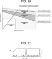
- FIG. 30 illustrates a modification example of the functions by the PWM mode switching unit 22.
- the regions of the PWM modes are divided by the "modulation rate output limit in synchronous PWM-X (X: any one of A to C)", but the regions of the PWM modes are set so as not to exceed the restriction of the minimum pulse width in each PWM mode.
- X any one of A to C
- the regions of the PWM modes are set so as not to exceed the restriction of the minimum pulse width in each PWM mode.
- four patterns A to C are described as an example, but the number of patterns is not limited.
- a configuration in which the PWM mode is driven by multi-pulse synchronous PWM may be made.
- the modulation rate is controlled by weak field control or the like.
- the drive apparatus for the rotating electrical machine to which the PWM control method according to Embodiment 3 is applied switches the PWM mode in accordance with the region defined in consideration of the restriction of the minimum pulse width with respect to the inverter frequency and the modulation rate, so that it is possible to accurately output the fundamental wave voltage at any frequency and modulation rate. As a result, it is possible to accurately output the voltage even at the time of the contact line voltage varying or at the time of restarting from coasting (free run).
Landscapes
- Engineering & Computer Science (AREA)
- Power Engineering (AREA)
- Inverter Devices (AREA)
- Control Of Ac Motors In General (AREA)
Applications Claiming Priority (2)
| Application Number | Priority Date | Filing Date | Title |
|---|---|---|---|
| JP2022132743 | 2022-08-23 | ||
| PCT/JP2023/026761 WO2024042942A1 (fr) | 2022-08-23 | 2023-07-21 | Appareil de commande d'entraînement et procédé de commande d'entraînement pour machine électrique tournante |
Publications (1)
| Publication Number | Publication Date |
|---|---|
| EP4580039A1 true EP4580039A1 (fr) | 2025-07-02 |
Family
ID=90013223
Family Applications (1)
| Application Number | Title | Priority Date | Filing Date |
|---|---|---|---|
| EP23857058.4A Pending EP4580039A1 (fr) | 2022-08-23 | 2023-07-21 | Appareil de commande d'entraînement et procédé de commande d'entraînement pour machine électrique tournante |
Country Status (3)
| Country | Link |
|---|---|
| EP (1) | EP4580039A1 (fr) |
| JP (1) | JP7736936B2 (fr) |
| WO (1) | WO2024042942A1 (fr) |
Family Cites Families (4)
| Publication number | Priority date | Publication date | Assignee | Title |
|---|---|---|---|---|
| JP4422567B2 (ja) * | 2004-06-30 | 2010-02-24 | 株式会社日立製作所 | モータ駆動装置,電動アクチュエータおよび電動パワーステアリング装置 |
| EP2040373B1 (fr) * | 2006-04-24 | 2013-06-19 | Panasonic Corporation | Dispositif d'inverseur et climatiseur |
| JP2011211818A (ja) * | 2010-03-30 | 2011-10-20 | Hitachi Ltd | 電力変換装置,電力変換方法及び電動機駆動システム |
| JP2012065481A (ja) * | 2010-09-17 | 2012-03-29 | Hitachi Ltd | Pwmインバータの制御装置およびpwmインバータの制御装置を備えた鉄道車両 |
-
2023
- 2023-07-21 WO PCT/JP2023/026761 patent/WO2024042942A1/fr not_active Ceased
- 2023-07-21 JP JP2024542662A patent/JP7736936B2/ja active Active
- 2023-07-21 EP EP23857058.4A patent/EP4580039A1/fr active Pending
Also Published As
| Publication number | Publication date |
|---|---|
| JP7736936B2 (ja) | 2025-09-09 |
| JPWO2024042942A1 (fr) | 2024-02-29 |
| WO2024042942A1 (fr) | 2024-02-29 |
Similar Documents
| Publication | Publication Date | Title |
|---|---|---|
| US8232753B2 (en) | Control device for electric motor drive apparatus | |
| US10291174B2 (en) | Control apparatus for power conversion apparatus | |
| US8278865B2 (en) | Control device | |
| US10199979B2 (en) | Power conversion device | |
| CN101529714B (zh) | 永磁同步电动机的矢量控制装置 | |
| US8030874B2 (en) | Power converting apparatus | |
| JP5683760B2 (ja) | 電力変換装置 | |
| US20110181231A1 (en) | Control device and control method for ac motor | |
| US11218107B2 (en) | Control device for power converter | |
| US11515809B2 (en) | Power conversion device and power conversion method | |
| WO2010103733A1 (fr) | Dispositif de conversion de puissance et son procédé de commande | |
| JP2015053824A (ja) | モータ駆動システムおよび該システムを搭載する電気鉄道車両 | |
| US20180219506A1 (en) | Ac rotary machine control device and electric power steering device | |
| US20160233800A1 (en) | Integrated circuit | |
| US11296630B2 (en) | Controller for rotary electric machine apparatus | |
| CN110168924A (zh) | 电动机控制装置 | |
| JP6399239B2 (ja) | 電力変換装置 | |
| JP2011239564A (ja) | 中性点クランプ式電力変換装置 | |
| EP4187774B1 (fr) | Dispositif de conversion de puissance et dispositif de direction assistée électrique | |
| EP3382889B1 (fr) | Dispositif de commande pour machine électrique et véhicule électrique l'utilisant | |
| US12132423B2 (en) | Controller for ac rotary electric machine and electric power steering apparatus | |
| EP4580039A1 (fr) | Appareil de commande d'entraînement et procédé de commande d'entraînement pour machine électrique tournante | |
| JP3788346B2 (ja) | 電圧形pwmインバータの制御装置 | |
| US12362697B2 (en) | Rotating electrical machine control device | |
| JP3609804B2 (ja) | インバータ制御装置 |
Legal Events
| Date | Code | Title | Description |
|---|---|---|---|
| STAA | Information on the status of an ep patent application or granted ep patent |
Free format text: STATUS: THE INTERNATIONAL PUBLICATION HAS BEEN MADE |
|
| PUAI | Public reference made under article 153(3) epc to a published international application that has entered the european phase |
Free format text: ORIGINAL CODE: 0009012 |
|
| STAA | Information on the status of an ep patent application or granted ep patent |
Free format text: STATUS: REQUEST FOR EXAMINATION WAS MADE |
|
| 17P | Request for examination filed |
Effective date: 20241119 |
|
| AK | Designated contracting states |
Kind code of ref document: A1 Designated state(s): AL AT BE BG CH CY CZ DE DK EE ES FI FR GB GR HR HU IE IS IT LI LT LU LV MC ME MK MT NL NO PL PT RO RS SE SI SK SM TR |
|
| DAV | Request for validation of the european patent (deleted) | ||
| DAX | Request for extension of the european patent (deleted) |