EP4580052A1 - Hochfrequenzbegrenzer - Google Patents
Hochfrequenzbegrenzer Download PDFInfo
- Publication number
- EP4580052A1 EP4580052A1 EP24223433.4A EP24223433A EP4580052A1 EP 4580052 A1 EP4580052 A1 EP 4580052A1 EP 24223433 A EP24223433 A EP 24223433A EP 4580052 A1 EP4580052 A1 EP 4580052A1
- Authority
- EP
- European Patent Office
- Prior art keywords
- limiter
- transistors
- lim1
- limn
- radiofrequency
- Prior art date
- Legal status (The legal status is an assumption and is not a legal conclusion. Google has not performed a legal analysis and makes no representation as to the accuracy of the status listed.)
- Pending
Links
Images






Classifications
-
- H—ELECTRICITY
- H03—ELECTRONIC CIRCUITRY
- H03F—AMPLIFIERS
- H03F3/00—Amplifiers with only discharge tubes or only semiconductor devices as amplifying elements
- H03F3/189—High-frequency amplifiers, e.g. radio frequency amplifiers
- H03F3/19—High-frequency amplifiers, e.g. radio frequency amplifiers with semiconductor devices only
- H03F3/195—High-frequency amplifiers, e.g. radio frequency amplifiers with semiconductor devices only in integrated circuits
-
- H—ELECTRICITY
- H03—ELECTRONIC CIRCUITRY
- H03F—AMPLIFIERS
- H03F1/00—Details of amplifiers with only discharge tubes, only semiconductor devices or only unspecified devices as amplifying elements
- H03F1/52—Circuit arrangements for protecting such amplifiers
- H03F1/523—Circuit arrangements for protecting such amplifiers for amplifiers using field-effect devices
-
- H—ELECTRICITY
- H03—ELECTRONIC CIRCUITRY
- H03G—CONTROL OF AMPLIFICATION
- H03G11/00—Limiting amplitude; Limiting rate of change of amplitude
- H03G11/006—Limiting amplitude; Limiting rate of change of amplitude in circuits having distributed constants
-
- H—ELECTRICITY
- H03—ELECTRONIC CIRCUITRY
- H03G—CONTROL OF AMPLIFICATION
- H03G11/00—Limiting amplitude; Limiting rate of change of amplitude
- H03G11/02—Limiting amplitude; Limiting rate of change of amplitude by means of diodes
-
- H—ELECTRICITY
- H03—ELECTRONIC CIRCUITRY
- H03F—AMPLIFIERS
- H03F2200/00—Indexing scheme relating to amplifiers
- H03F2200/211—Indexing scheme relating to amplifiers the input of an amplifier can be attenuated by a continuously controlled transistor attenuator
-
- H—ELECTRICITY
- H03—ELECTRONIC CIRCUITRY
- H03F—AMPLIFIERS
- H03F2200/00—Indexing scheme relating to amplifiers
- H03F2200/294—Indexing scheme relating to amplifiers the amplifier being a low noise amplifier [LNA]
-
- H—ELECTRICITY
- H03—ELECTRONIC CIRCUITRY
- H03F—AMPLIFIERS
- H03F2200/00—Indexing scheme relating to amplifiers
- H03F2200/444—Diode used as protection means in an amplifier, e.g. as a limiter or as a switch
-
- H—ELECTRICITY
- H03—ELECTRONIC CIRCUITRY
- H03F—AMPLIFIERS
- H03F2200/00—Indexing scheme relating to amplifiers
- H03F2200/451—Indexing scheme relating to amplifiers the amplifier being a radio frequency amplifier
Definitions
- the invention relates to the field of radiofrequency power limiters, used in particular in radiofrequency transmission/reception (T/R) modules of airborne systems.
- T/R radiofrequency transmission/reception
- the power limiter is a device whose objective is to clip its output power in the presence of high input power levels.
- LNA low noise amplifiers
- LNA - Low Noise Amplifier its use has become essential to protect against possible attacks (intentional or not) from increasingly powerful electromagnetic sources ( Figure 1 ).
- LNAs are generally made using AsGa, Si or, more recently, GaN technologies. AsGa and Si technologies allow for reduced noise levels but do not allow for excessively high power levels (around 0.5 W).
- Limiters are generally made from PIN and/or Shottky diodes. These diodes have the advantage of being low cost while offering good power handling.
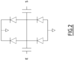
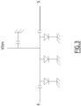
- the most commonly used limiter structures using PIN and/or Shottky diodes are generally based on "head-to-tail" diode architectures ( Figure 2 ) in order to clip the positive half-wave and the negative half-wave of the signal, or on parallel diode architectures ( Figure 3 ). In both cases, these architectures use the non-linearity of the diodes to reflect and therefore clip the RF signal from a certain power level.
- [1] presents a solution to meet the needs mentioned above. It describes an MMIC limiter made in GaN technology from field effect transistors not polarized between their drain and their source, called cold FETs (FET for “Field Effect Transistor”). These transistors are placed in parallel between the RF input and the RF output of the limiter and alternately with self-inductors (placed in series between the RF input and the RF output).
- FET Field Effect Transistor
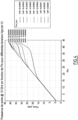
- the structure described in [1] has the disadvantage of not sufficiently clipping its output power in RX mode (reception mode in which the limiter must both protect the LNA and present the lowest possible insertion losses to guarantee the performance of the RX chain). Indeed, as illustrated in Figure 4 , in RX mode, when the Pin input power increases (in the presence of an attack, for example), the Pout output power does not reach a plateau, and continues to increase. The limitation level is not sufficient. Indeed, it is advisable not to exceed 20 dBm at the output, so as not to damage the low noise amplifiers in the reception chain which would be made of AsGa.
- An object of the invention is therefore a radiofrequency limiter, comprising an input port, an output port, a plurality of transistors connected in parallel between the input port and the output port, the transistors being configured to be biased only between their gate and their source during operation of the limiter, and a plurality of self-inductances, connected in series between the input port and the output port, alternately with each of the transistors, each transistor gate being connected to a voltage source via an adjustment resistor, a diode being connected between each drain and each adjustment resistor.
- the anode of the diode is connected between two self-inductances, and the cathode of the diode is connected to the adjustment resistor.
- the voltage source is configured to apply a voltage close to the transistor pinch-off voltage at the gate of each transistor.
- a protective resistor is connected directly, on the one hand, to the gate of the transistor and, on the other hand, to the diode and the adjustment resistor.
- the limiter is integrated in high-power MMIC technology based on Gallium Nitride (GaN).
- GaN Gallium Nitride
- the adjustment resistors do not all have the same value.
- the value of the adjustment resistor closest to the input port is greater than the values of the other adjustment resistors.
- the invention also relates to a transmission/reception module, comprising a aforementioned radiofrequency limiter.
- the invention also relates to the use of the aforementioned radiofrequency limiter or the aforementioned transmission/reception module, as a variable attenuation pad controllable by varying the voltage generated by the voltage source.
- the voltage range varies between the transistors' pinch-off voltage and 0 V.
- the IN input port is a connection point that allows the signal to be received at the output of the circulator.
- the OUT output port is another connection point that allows the limited signal to be made available to the low noise amplifiers LNA of the receiving channel.
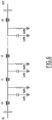
- the limiter comprises a plurality of cells (Cell1...CellN) connected in parallel, as well as a plurality of self-inductances (L1...LN) connected in series, alternating with the cells.
- Cell1...CellN a plurality of cells connected in parallel
- L1...LN a plurality of self-inductances
- each transistor is connected to the control potential VLim, the value of which will modulate the attenuation level.
- Protective resistors R G1 ...R GN
- T1...TN the gate of the transistor
- each detection diode (Det1...DetN) is connected to the voltage source (VLim) via an adjustment resistor (R Lim1 ...R LimN ) which allows the function limitation level to be adjusted, as shown below.
- each detection diode (Det1... DetN) is connected between the drain of the transistor and an adjustment resistor (R Lim1 ... R LimN ).
- the anode of the diode (Det1...
- DetN is connected between two self-inductances (L1...LN), and the cathode of the diode (Det1...DetN) is connected to the gate of the transistor (T1...TN) (possibly via the protection resistor (R G1 ...R GN )), and to the adjustment resistor (R Lim1 ... R LimN ).
- the limiter end inductors and capacitors, immediately adjacent to the input port and output port, are shown to account for input and output wiring leads, which can introduce parasitic inductances and capacitances.
- the limiter is equivalent to a transmission line.
- Each cell is then equivalent to a resistance Roff (resistance causing insertion losses) and a capacitance Coff in parallel (parasitic capacitance limiting the operating frequency), as illustrated in Figure 6
- Roff resistance causing insertion losses
- Coff capacitance limiting the operating frequency
- the detection diodes will start to conduct and will change the gate bias of the transistors.
- the voltage seen by each of the gates will be equal to VLim - RLim.I Diode with VLim the control voltage and I Diode the current flowing through each diode.
- the transistors will then gradually move from a blocked state (high impedance) to a passing state (low impedance) thus increasing the insertion losses, and giving a compression appearance to the limiter, similar to what is obtained on an amplifier.
- the equivalent model of the limiter at the end of the variation range of the input pin is then equivalent to that described in the diagram of the Figure 7 .
- the adjustment resistors (R Lim1 ... R LimN ) do not all have the same value, which makes it possible to trigger the change of state of the cells at different times.
- the value of the adjustment resistor R Lim1 closest to the input port IN is higher than the values of the other adjustment resistors (R Lim2 ...R LimN ). Indeed, the first cell Cell1 is driven by the highest power. It is therefore advantageous to have a higher resistance value for this cell.
- FIG. 9 illustrates the transmission response and input/output reflection coefficients at low RF power levels of the limiter when the limiter is in RX mode.
- the limiter architecture provides a response substantially identical to that of a transmission line below the structure cutoff frequency, with transmission losses below 1.4 dB over 6 GHz of band, as well as excellent adaptation to RF accesses in this operating band.
- the limiter in RX mode (reception mode), the limiter must have the lowest possible insertion losses to guarantee the performance of the reception chain, while protecting the low noise amplifiers LNA in the event of an attack.
- FIG. 10 shows the transmission response and the RF input/output reflection coefficients at low level (in the linear operating zone) of the limiter when it is in TX mode (maximum attenuation).
- the attenuation level is approximately 48 dB, which allows the low noise amplifiers LNA of the RX chain to be well isolated from the HPA amplifiers of the TX chain when the latter are transmitting.
- FIG. 11 illustrates the evolution of the insertion losses as well as the output power of the limiter according to the invention as a function of the input power Pin in TX mode and for frequencies between 6 and 12 GHz. These results are obtained for a voltage VLim applied between the gate and the source of the transistors T1...TN equal to 0 V.
- the gain curve illustrates the fact that the attenuation is constant, independently of the frequency or the input power.
- the invention also makes it possible to use the radiofrequency limiter as a variable attenuation pad by applying a voltage VLim between 0 and Vp.
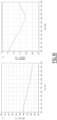
- FIG. 12 shows the evolution of the output power as a function of the input power (left figure) as well as the transmission response (gain, right figure) of the limiter according to the invention for different voltage levels VLim corresponding to different attenuation levels.
- the limiter can integrate this functionality brings several advantages. First, it saves the need for a variable attenuator that would potentially need to be added, which increases the level of integration. Second, it improves the performance of the RX chain because this additional functionality saves the insertion losses of an additional component.
- the radiofrequency limiter according to the invention can be integrated into high-power MMIC technology based on Gallium Nitride (GaN), which makes it possible to offer good power handling and a high level of integration.
- GaN Gallium Nitride
- the invention also relates to the use of the aforementioned radiofrequency limiter, as a variable attenuation pad controllable by varying the voltage VLim generated by the voltage source.
Landscapes
- Engineering & Computer Science (AREA)
- Power Engineering (AREA)
- Microelectronics & Electronic Packaging (AREA)
- Tone Control, Compression And Expansion, Limiting Amplitude (AREA)
Applications Claiming Priority (1)
| Application Number | Priority Date | Filing Date | Title |
|---|---|---|---|
| FR2315421A FR3157968A1 (fr) | 2023-12-28 | 2023-12-28 | Limiteur radiofréquence |
Publications (1)
| Publication Number | Publication Date |
|---|---|
| EP4580052A1 true EP4580052A1 (de) | 2025-07-02 |
Family
ID=91334876
Family Applications (1)
| Application Number | Title | Priority Date | Filing Date |
|---|---|---|---|
| EP24223433.4A Pending EP4580052A1 (de) | 2023-12-28 | 2024-12-27 | Hochfrequenzbegrenzer |
Country Status (2)
| Country | Link |
|---|---|
| EP (1) | EP4580052A1 (de) |
| FR (1) | FR3157968A1 (de) |
Citations (2)
| Publication number | Priority date | Publication date | Assignee | Title |
|---|---|---|---|---|
| FR3013536A1 (fr) * | 2013-11-18 | 2015-05-22 | Thales Sa | Limiteur de puissance radiofrequence ameliore; chaine d'emission et/ou de reception radiofrequence et etage d'amplification faible bruit associes |
| CN115549620A (zh) * | 2022-09-23 | 2022-12-30 | 上海华虹宏力半导体制造有限公司 | 限幅器电路 |
-
2023
- 2023-12-28 FR FR2315421A patent/FR3157968A1/fr active Pending
-
2024
- 2024-12-27 EP EP24223433.4A patent/EP4580052A1/de active Pending
Patent Citations (3)
| Publication number | Priority date | Publication date | Assignee | Title |
|---|---|---|---|---|
| FR3013536A1 (fr) * | 2013-11-18 | 2015-05-22 | Thales Sa | Limiteur de puissance radiofrequence ameliore; chaine d'emission et/ou de reception radiofrequence et etage d'amplification faible bruit associes |
| FR3013536B1 (fr) | 2013-11-18 | 2016-01-01 | Thales Sa | Limiteur de puissance radiofrequence ameliore; chaine d'emission et/ou de reception radiofrequence et etage d'amplification faible bruit associes |
| CN115549620A (zh) * | 2022-09-23 | 2022-12-30 | 上海华虹宏力半导体制造有限公司 | 限幅器电路 |
Non-Patent Citations (1)
| Title |
|---|
| MATHIEU R ET AL: "A 450W GaN-Based Limiter for S-Band Applications", 2023 IEEE/MTT-S INTERNATIONAL MICROWAVE SYMPOSIUM - IMS 2023, IEEE, 11 June 2023 (2023-06-11), pages 174 - 177, XP034385584, DOI: 10.1109/IMS37964.2023.10188180 * |
Also Published As
| Publication number | Publication date |
|---|---|
| FR3157968A1 (fr) | 2025-07-04 |
Similar Documents
| Publication | Publication Date | Title |
|---|---|---|
| US10749490B1 (en) | PIN diode bias scheme to improve leakage characteristics and P1dB threshold level of reflective limiter device | |
| FR2921213A1 (fr) | Systemes, procedes, et appareils pour commutateurs d'antenne haute puissance a semi-conducteur a oxyde de metal complementaire(cmos) utilisant la commutation de corps et un composant externe dans une structure a empilages multiples | |
| FR2873247A1 (fr) | Emetteur radio avec adaptation d'impedance variable | |
| FR2959077A1 (fr) | Amplificateur a faible facteur de bruit, a gain variable et de puissance | |
| FR2829316A1 (fr) | Attenuateur commande | |
| US20230275549A1 (en) | Voltage controlled attenuator | |
| EP2120280A1 (de) | Hyperfrequenzumschalter und mit einem solchen Umschalter ausgestattetes Sende- und Empfangsmodul | |
| FR3157968A1 (fr) | Limiteur radiofréquence | |
| US8836430B1 (en) | Wideband distributed amplifier with integral bypass | |
| EP0978949B1 (de) | Schalter für Funkfrequenzsignale | |
| EP2182631A2 (de) | Mikrowellen-Breitband-Verstärkerzelle mit regelbarer Verstärkung und eine solche Zelle umfassender Verstärker | |
| EP3072234A1 (de) | Verbesserter hochfrequenzleistungsbegrenzer und zugehörige hochfrequenzsender- und/oder -empfängerkette sowie rauscharme verstärkerstufe | |
| FR2902250A1 (fr) | Commutateur et dispositif de commutation a isolation selective pour terminaux multimedias | |
| EP0420106B1 (de) | Attenuatorschaltung mit einem Dual-Gate-Feldeffekttransistor | |
| EP0372643B1 (de) | Integrierte Halbleiterschaltung mit einer Leistungsverstärkerstufe für Ultrahochfrequenz | |
| FR3066058B1 (fr) | Appareil de communication avec une isolation renforcee de la chaine de reception | |
| US20060293020A1 (en) | Radio frequency receiver including a limiter and related methods | |
| FR3048831A1 (fr) | Chaine de reception amelioree; module d'emission-reception comportant une telle chaine de reception | |
| EP2420858A1 (de) | In LNA integrierter PIN-Dioden-Limiter | |
| EP2993798B1 (de) | Sendemodul und entsprechendes verfahren zur umsetzung multipler betriebsmodi | |
| EP2168242A1 (de) | Aktives schaltbauelement und integrierte hyperfrequenzschaltung mit einem solchen bauelement | |
| EP0446828A1 (de) | Limiter mit einem Feldeffekttransistor | |
| EP4643455A1 (de) | Verstärkungsvorrichtung mit doppelfunktion für eine aktive antenne | |
| FR3091081A1 (fr) | Amplificateur à forte puissance et à large bande de fréquences | |
| EP4020821A1 (de) | System zur anpassung der spannung eines drains einer leistungsstufe |
Legal Events
| Date | Code | Title | Description |
|---|---|---|---|
| PUAI | Public reference made under article 153(3) epc to a published international application that has entered the european phase |
Free format text: ORIGINAL CODE: 0009012 |
|
| STAA | Information on the status of an ep patent application or granted ep patent |
Free format text: STATUS: THE APPLICATION HAS BEEN PUBLISHED |
|
| AK | Designated contracting states |
Kind code of ref document: A1 Designated state(s): AL AT BE BG CH CY CZ DE DK EE ES FI FR GB GR HR HU IE IS IT LI LT LU LV MC ME MK MT NL NO PL PT RO RS SE SI SK SM TR |
|
| STAA | Information on the status of an ep patent application or granted ep patent |
Free format text: STATUS: REQUEST FOR EXAMINATION WAS MADE |
|
| 17P | Request for examination filed |
Effective date: 20251215 |