EP4580357A1 - Dispositif électroluminescent et dispositif électronique comprenant le dispositif électroluminescent - Google Patents
Dispositif électroluminescent et dispositif électronique comprenant le dispositif électroluminescent Download PDFInfo
- Publication number
- EP4580357A1 EP4580357A1 EP24222954.0A EP24222954A EP4580357A1 EP 4580357 A1 EP4580357 A1 EP 4580357A1 EP 24222954 A EP24222954 A EP 24222954A EP 4580357 A1 EP4580357 A1 EP 4580357A1
- Authority
- EP
- European Patent Office
- Prior art keywords
- group
- compound
- light
- emitting device
- substituted
- Prior art date
- Legal status (The legal status is an assumption and is not a legal conclusion. Google has not performed a legal analysis and makes no representation as to the accuracy of the status listed.)
- Pending
Links
Images
Classifications
-
- H—ELECTRICITY
- H10—SEMICONDUCTOR DEVICES; ELECTRIC SOLID-STATE DEVICES NOT OTHERWISE PROVIDED FOR
- H10K—ORGANIC ELECTRIC SOLID-STATE DEVICES
- H10K50/00—Organic light-emitting devices
- H10K50/10—OLEDs or polymer light-emitting diodes [PLED]
- H10K50/11—OLEDs or polymer light-emitting diodes [PLED] characterised by the electroluminescent [EL] layers
- H10K50/12—OLEDs or polymer light-emitting diodes [PLED] characterised by the electroluminescent [EL] layers comprising dopants
- H10K50/121—OLEDs or polymer light-emitting diodes [PLED] characterised by the electroluminescent [EL] layers comprising dopants for assisting energy transfer, e.g. sensitization
-
- H—ELECTRICITY
- H10—SEMICONDUCTOR DEVICES; ELECTRIC SOLID-STATE DEVICES NOT OTHERWISE PROVIDED FOR
- H10K—ORGANIC ELECTRIC SOLID-STATE DEVICES
- H10K50/00—Organic light-emitting devices
- H10K50/10—OLEDs or polymer light-emitting diodes [PLED]
- H10K50/14—Carrier transporting layers
- H10K50/15—Hole transporting layers
-
- H—ELECTRICITY
- H10—SEMICONDUCTOR DEVICES; ELECTRIC SOLID-STATE DEVICES NOT OTHERWISE PROVIDED FOR
- H10K—ORGANIC ELECTRIC SOLID-STATE DEVICES
- H10K85/00—Organic materials used in the body or electrodes of devices covered by this subclass
- H10K85/60—Organic compounds having low molecular weight
- H10K85/631—Amine compounds having at least two aryl rest on at least one amine-nitrogen atom, e.g. triphenylamine
- H10K85/636—Amine compounds having at least two aryl rest on at least one amine-nitrogen atom, e.g. triphenylamine comprising heteroaromatic hydrocarbons as substituents on the nitrogen atom
-
- H—ELECTRICITY
- H10—SEMICONDUCTOR DEVICES; ELECTRIC SOLID-STATE DEVICES NOT OTHERWISE PROVIDED FOR
- H10K—ORGANIC ELECTRIC SOLID-STATE DEVICES
- H10K2101/00—Properties of the organic materials covered by group H10K85/00
- H10K2101/20—Delayed fluorescence emission
-
- H—ELECTRICITY
- H10—SEMICONDUCTOR DEVICES; ELECTRIC SOLID-STATE DEVICES NOT OTHERWISE PROVIDED FOR
- H10K—ORGANIC ELECTRIC SOLID-STATE DEVICES
- H10K2101/00—Properties of the organic materials covered by group H10K85/00
- H10K2101/30—Highest occupied molecular orbital [HOMO], lowest unoccupied molecular orbital [LUMO] or Fermi energy values
-
- H—ELECTRICITY
- H10—SEMICONDUCTOR DEVICES; ELECTRIC SOLID-STATE DEVICES NOT OTHERWISE PROVIDED FOR
- H10K—ORGANIC ELECTRIC SOLID-STATE DEVICES
- H10K2101/00—Properties of the organic materials covered by group H10K85/00
- H10K2101/40—Interrelation of parameters between multiple constituent active layers or sublayers, e.g. HOMO values in adjacent layers
-
- H—ELECTRICITY
- H10—SEMICONDUCTOR DEVICES; ELECTRIC SOLID-STATE DEVICES NOT OTHERWISE PROVIDED FOR
- H10K—ORGANIC ELECTRIC SOLID-STATE DEVICES
- H10K85/00—Organic materials used in the body or electrodes of devices covered by this subclass
- H10K85/30—Coordination compounds
- H10K85/341—Transition metal complexes, e.g. Ru(II)polypyridine complexes
- H10K85/346—Transition metal complexes, e.g. Ru(II)polypyridine complexes comprising platinum
-
- H—ELECTRICITY
- H10—SEMICONDUCTOR DEVICES; ELECTRIC SOLID-STATE DEVICES NOT OTHERWISE PROVIDED FOR
- H10K—ORGANIC ELECTRIC SOLID-STATE DEVICES
- H10K85/00—Organic materials used in the body or electrodes of devices covered by this subclass
- H10K85/60—Organic compounds having low molecular weight
- H10K85/649—Aromatic compounds comprising a hetero atom
- H10K85/657—Polycyclic condensed heteroaromatic hydrocarbons
- H10K85/6572—Polycyclic condensed heteroaromatic hydrocarbons comprising only nitrogen in the heteroaromatic polycondensed ring system, e.g. phenanthroline or carbazole
-
- H—ELECTRICITY
- H10—SEMICONDUCTOR DEVICES; ELECTRIC SOLID-STATE DEVICES NOT OTHERWISE PROVIDED FOR
- H10K—ORGANIC ELECTRIC SOLID-STATE DEVICES
- H10K85/00—Organic materials used in the body or electrodes of devices covered by this subclass
- H10K85/60—Organic compounds having low molecular weight
- H10K85/649—Aromatic compounds comprising a hetero atom
- H10K85/657—Polycyclic condensed heteroaromatic hydrocarbons
- H10K85/6574—Polycyclic condensed heteroaromatic hydrocarbons comprising only oxygen in the heteroaromatic polycondensed ring system, e.g. cumarine dyes
-
- H—ELECTRICITY
- H10—SEMICONDUCTOR DEVICES; ELECTRIC SOLID-STATE DEVICES NOT OTHERWISE PROVIDED FOR
- H10K—ORGANIC ELECTRIC SOLID-STATE DEVICES
- H10K85/00—Organic materials used in the body or electrodes of devices covered by this subclass
- H10K85/60—Organic compounds having low molecular weight
- H10K85/658—Organoboranes
Definitions
- Organic light-emitting devices are self-emissive devices that have wide viewing angles, high contrast ratios, short response times, and excellent characteristics in terms of luminance, driving voltage, and response speed, to provide full-color images.
- An organic light-emitting device includes an anode, a cathode, and an emission layer arranged between the anode and the cathode.
- a hole transport region may be provided between the anode and the emission layer, and an electron transport region may be provided between the emission layer and the cathode.
- Holes provided from the anode move toward the emission layer through the hole transport region, and electrons provided from the cathode move toward the emission layer through the electron transport region.
- the holes and the electrons recombine in the emission layer to produce excitons.
- the excitons may transition from an excited state to a ground state and in the process emit light of a given wavelength range.
- a light-emitting device includes:
- the HOMO energy level of the additional compound(s) is also a negative number calculated based on DFT.
- the HOMO energy level of the additional compound(s) is evaluated using the DFT method (T1 adiabatic) of the Gaussian program which is structurally optimized at the B3LYP/6-31G(d,p) level, as described in Evaluation Example 1, and may be a negative value.
- each of the HOMO energy level and lowest unoccupied molecular orbital (LUMO) energy level may be calculated based on DFT and may be a negative value.
- Holes injected from the first electrode migrate to the emission layer through the hole transport region.
- accumulation of holes inside the emission layer and/or at the interface between the emission layer and the hole transport region causes a decrease in the luminescence efficiency and/or lifespan of the light-emitting device.
- the improvement in the capacitance of the light-emitting device may minimize such accumulation of holes within the emission layer and/or at the interface.
- the ⁇ HOMO of the light-emitting device is less than 0 eV as in Condition 1, that is, the HOMO energy level of the first material included in the first layer is less than the HOMO energy level of the first compound included in the emission layer (or when the HOMO energy level of the first material included in the first layer is deeper than the HOMO energy level of the first compound included in the emission layer), injection of holes from the first electrode into the emission layer may not proceed smoothly.
- the dipole moment of the first material included in the first layer is a relatively small value, i.e., less than 3.0 debye as in Condition 1 the energetic disorder of the first layer may be reduced and hole mobility in the first layer may be increased.
- injection and transport of holes may be performed at suitable speed, and thereby accumulation of holes within the emission layer and/or at the interface between the emission layer and the hole transport region can be relatively minimized or substantially prevented during operation (driving) of the light-emitting device.
- the ⁇ HOMO of the light-emitting device is greater than 0 eV as in Condition 2, that is, the HOMO energy level of the first material included in the first layer is greater than the HOMO energy level of the first compound included in the emission layer (or when the HOMO energy level of the first material included in the first layer is shallower than the HOMO energy level of the first compound included in the emission layer), injection of holes from the first electrode into the emission layer may proceed relatively smoothly.
- the dipole moment of the first material included in the first layer is a relatively large value of 3.0 debye or more as in Condition 2, the energetic disorder of the first layer may increase and hole mobility in the first layer may be reduced.
- injection and transport of holes may be performed at suitable speed, and thereby accumulation of holes within the emission layer and/or at the interface between the emission layer and the hole transport region can be relatively minimized or substantially prevented during operation (driving) of the light-emitting device.
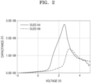
- the light-emitting device satisfies Condition 1 or Condition 2 as described above, hole accumulation inside (within) the emission layer and/or at the interface between the emission layer and the hole transport region is substantially minimized or prevented during the operation of the light-emitting device and the capacitance characteristics of the light-emitting device can be improved.
- high-quality electronic devices can be manufactured by using the light-emitting devices described herein.
- values, without a unit, obtained by multiplying the value obtained by subtracting 3 debye from the dipole moment of the first material by ⁇ HOMO may be 0.0 or a positive number (for example, 0.0 or more (greater) and 0.7 or less).
- the light-emitting device may satisfy Condition 1, and ⁇ HOMO may be about -0.5 eV or more and less than about 0 eV, about -0.5 eV or more and less than about -0.001 eV, about -0.5 eV or more and less than about -0.005 eV, about -0.5 eV or more and less than about -0.01 eV, about -0.5 eV or more and less than about -0.052 eV, about -0.4 eV or more and less than about 0 eV, about -0.4 eV or more and less than about -0.001 eV, about -0.4 eV or more and less than about -0.005 eV, about -0.4 eV or more and less than about -0.01 eV, about -0.4 eV or more and less than about -0.052 eV, about -0.310 eV or more and less than about 0 eV, about -
- the light-emitting device may satisfy Condition 1, and the dipole moment of the first material may be about 0.5 debye or more and less than about 3.0 debye, about 0.8 debye or more and less than about 3.0 debye, about 1.0 debye or more and less than about 3.0 debye, about 1.2 debye or more and less than about 3.0 debye, about 1.341 debye or more and less than about 3.0 debye, about 0.5 debye or more and less than about 2.9 debye, about 0.8 debye or more and less than about 2.9 debye, about 1.0 debye or more and less than about 2.9 debye, about 1.2 debye or more and less than about 2.9 debye, about 1.341 debye or more and less than about 2.9 debye, about 0.5 debye or more and less than about 2.805 debye, about 0.8 debye or more and less than about 2.805 debye, about 1.0 debybye or more and less than
- the light-emitting device may satisfy Condition 2, and ⁇ HOMO may be more than 0 eV and about 0.1 eV or less, more than 0 eV and about 0.06 eV or less, more than 0 eV and about 0.043 eV or less, about 0.0001 eV or more and about 0.1 eV or less, about 0.0001 eV or more and about 0.06 eV or less, about 0.0001 eV or more and about 0.043 eV or less, about 0.001 eV or more and about 0.1 eV or less, about 0.001 eV or more and about 0.06 eV or less, or about 0.001 eV or more and about 0.043 eV or less.
- the HOMO energy level of the first compound included in the emission layer may be about -5.6 eV to about -4.8 eV, about -5.6 eV to about -4.9 eV, about -5.6 eV to about -5.0 eV, about -5.5 eV to about -4.8 eV, about -5.5 eV to about -4.9 eV, about -5.5 eV to about -5.0 eV, about -5.4 eV to about -4.8 eV, about -5.4 eV to about -4.9 eV, about -5.4 eV to about -5.07 eV, or about -5.419 eV to about -5.066 eV.
- the HOMO energy level of the first material included in the first layer may be about -5.6 eV to about -4.8 eV, about -5.6 eV to about -4.9 eV, about -5.6 eV to about -5.0 eV, about -5.5 eV to about -4.8 eV, about -5.5 eV to about -4.9 eV, about -5.5 eV to about -5.0 eV, about -5.4 eV to about -4.8 eV, about -5.4 eV to about -4.9 eV, about -5.4 eV to about -5.07 eV, or about -5.419 eV to about -5.066 eV.
- the dipole moment of the first material included in the first layer may be about 0.8 debye to about 7.0 debye, about 0.8 debye to about 6.0 debye, about 0.8 debye to about 5.1 debye, about 1.0 debye to about 6.0 debye, about 1.0 debye to about 5.1 debye, about 1.2 debye to about 6.0 debye, about 1.2 debye to about 5.1 debye, about 1.3 debye to about 6.0 debye, about 1.3 debye to about 5.1 debye, or about 1.341 debye to about 5.008 debye.
- each of the first compound included in the emission layer and the first material included in the first layer may not include an amine moiety.
- the organometallic compound included in the emission layer may further include n ligands bonded to the transition metal, the transition metal in the organometallic compound may be platinum (Pt) or palladium (Pd), n may be 1, and the ligand may be a tetradentate ligand.
- the tetradentate ligand may include a carbene moiety coordinated to the transition metal.
- the tetradentate ligand may include a carbene moiety of an imidazole group, or of a benzimidazole group, coordinated to the transition metal.
- the organometallic compound included in the emission layer may further include n ligands bonded to the transition metal, the transition metal in the organometallic compound may be iridium (Ir) or osmium (Os), n may be 3, and at least one of the n ligands may be a bidentate ligand including -F substituent, a cyano substituent, or a combination thereof, or a bidentate ligand including a carbene moiety bonded to the transition metal.
- the bidentate ligand may further include an imidazole group, benzimidazole group, or a triazole group.
- the second compound may be a compound including at least one electron-transporting moiety.
- the electron-transporting moiety may be a cyano group, a fluoro group, a ⁇ electron-deficient nitrogen-containing C 1 -C 60 cyclic group (for example, a triazine group, a pyrimidine group, etc.), a phosphine oxide group, a sulfoxide group, or a combination thereof.
- R 1 to R 7 may each independently be:
- R 1 to R 7 in Formulae 1-1, 1-2 and 1-3 may each independently be:
- R 1 to R 7 in Formulae 1-1, 1-2 and 1-3 may each independently be:
- each of i) R 1 , ii) R 3 , iii) R 4 , or iv) R 3 and R 4 , in Formula 1-1 may be a group represented by Formula S-1.
- R 6 in Formula 1-2 may be a group represented by Formula S-1.
- rings A 1 to rings A 7 and rings B 1 to rings B 4 in Formulae 1-1, 1-2, 1-3, and S-1 may each independently be a benzene group, a naphthalene group, a furan group, a thiophene group, a pyrrole group, a cyclopentadiene group, a silole group, a benzofuran group, a benzothiophene group, an indole group, an indene group, a benzosilole group, a dibenzofuran group, a dibenzothiophene group, a carbazole group, a fluorene group, a dibenzosilole group, a benzofurocarbazole group, a benzothienocarbazole group, an indolocarbazole group, an indenocarbazole group, or a benzosilolocarbazole group.
- rings A 1 , A 2 , A 4 and A 5 may each independently be a benzene group, a benzofuran group, a benzothiophene group, or an indole group.
- rings A 3 , A 6 and A 7 , and rings B 1 to ring B 4 may each independently be a benzene group, a dibenzofuran group, a dibenzothiophene group, a carbazole group, a benzofurocarbazole group, a benzothienocarbazole group, or an indolocarbazole group.
- the organometallic compound included in the emission layer in the present specification may be an organometallic compound represented by Formula 3: wherein, in Formula 3,
- M 31 in Formula 3 may be Pt, Pd, or Au.
- M 31 in Formula 3 may be Pt or Pd.
- the bond between X 11 and M 31 in Formula 3 may be a coordinate bond.
- ring CY 31 to ring CY 34 in Formula 3 may each independently be i) a first ring, ii) a second ring, iii) a condensed ring in which two or more first rings are condensed with each other, iv) a condensed ring in which two or more second rings are condensed with each other, or v) a condensed ring in which at least one first ring is condensed with at least one second ring,
- ring CY 33 in Formula 3 may be a benzene group, a naphthalene group, a pyridine group, a pyrimidine group, a pyridazine group, a pyrazine group, a benzene group to which an adamantane group is condensed, a benzene group to which a norbornane group is condensed, a carbazole group, a dibenzofuran group, a dibenzothiophene group, a benzocarbazole group, a naphthocarbazole group, an azacarbazole group, an azadibenzofuran group, an azadibenzothiophene group, an azabenzocarbazole group, or an azanaphthocarbazole group.
- T 31 in Formula 3 may be *-S-*' or *-O-*'.
- each of T 32 and T 33 in Formula 3 may be a single bond.
- X 11 , X 12 , and X 13 may be C, and X 14 may be N.
- R 31 to R 34 , R 35a , R 35b , R 36a , R 36b , R 37a , R 37b , R 38a , and R 38b may each independently be:
- the organometallic compound represented by Formula 3 may be an organometallic compound represented by Formula 3-1 or an organometallic compound represented by Formula 3-2:
- the bond between the carbon of the imidazole group and M 31 may be a coordinate bond. That is, the imidazole group in Formula 3-1 may include a carbene moiety bonded to M 31 .
- the bond between the carbon of the benzimidazole group and M 31 may be a coordinate bond. That is, the benzimidazole group in Formula 3-2 may include a carbene moiety bonded to M 31 .
- Formula 3-1' in which the carbon bonded to M 31 in the imidazole group is carbene, is the same as Formula 3-1
- Formula 3-2' in which the carbon bonded to M 31 in the benzimidazole group is carbene is the same as Formula 3-2: wherein, in Formulae 3-1 and 3-2,
- the organometallic compound represented by Formula 3 may be an organometallic compound represented by Formula 3-1(1) or an organometallic compound represented by Formula 3-2(1): In Formulae 3-1(1) and 3-2(1),
- the organometallic compound included in the emission layer in the present specification may be an organometallic compound represented by Formula 5: Formula 5 M 51 (L 51 ) n51 (L 52 ) n52 .
- M 51 in Formula 5 may be a transition metal.
- M 51 may be a first-row transition metal, a second-row transition metal, or a third-row transition metal of the Periodic Table of Elements.
- Y 51 to Y 54 in Formulae 5A to 5B may each independently be C or N.
- Y 51 and Y 53 may each be N
- Y 52 and Y 54 may each be C.
- the thermally activated delayed fluorescent material (for example, the polycyclic compound represented by Formula 4) may be selected from Compounds D1 to D30:
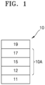
- FIG. 1 schematically shows a cross-sectional view of an organic light-emitting device 10, which is one of light-emitting devices according to embodiments of the present disclosure.
- an organic light-emitting device 10 which is one of light-emitting devices according to embodiments of the present disclosure.
- FIG. 1 schematically shows a cross-sectional view of an organic light-emitting device 10, which is one of light-emitting devices according to embodiments of the present disclosure.
- the structure and manufacturing method of an organic light-emitting device according to an embodiment of the present disclosure will be described in accordance with the FIG. 1 .
- the organic light-emitting device 10 of FIG. 1 includes a first electrode 11, a second electrode 19 facing the first electrode 11, and an interlayer 10A disposed between the first electrode 11 and the second electrode 19.
- the interlayer 10A may include an emission layer 15, a hole transport region 12 disposed between the first electrode 11 and the emission layer 15, and an electron transport region 17 disposed between the emission layer 15 and the second electrode 19.
- the hole transport region 12 may further include a first layer (not shown in FIG. 1 ). The first layer may directly contact the emission layer 15.
- a substrate may be additionally disposed under the first electrode 11 or above the second electrode 19.
- the substrate may be a conventional substrate used in organic light-emitting devices, for example, a glass substrate or a transparent plastic substrate, each having excellent mechanical strength, thermal stability, transparency, surface smoothness, ease of handling, and water repellency.
- the first electrode 11 may be formed by, for example, depositing or sputtering, onto the substrate, a material for forming the first electrode 11.
- the first electrode 11 may be an anode.
- the material for forming the first electrode 11 may include materials with a high work function to facilitate hole injection.
- the material for forming the first electrode 11 may include magnesium (Mg), silver (Ag), aluminum (Al), aluminum-lithium (Al-Li), calcium (Ca), magnesium-indium (Mg-In), magnesium-silver (Mg-Ag), or a combination thereof.
- the first electrode 11 may have a single-layer structure or a multi-layer structure including a plurality of layers.
- a thickness of the emission layer 15 may be in a range of about 100 ⁇ to about 1,000 ⁇ , for example, about 200 ⁇ to about 600 ⁇ . When the thickness of the emission layer 15 is within these ranges, excellent light-emission characteristics may be obtained without a substantial increase in driving voltage.
- the emission layer 15 may include a first compound and an organometallic compound as described herein. Additionally, the emission layer 15 may further include at least one of a second compound and a thermally activated delayed fluorescent material in addition to the first compound and the organometallic compound.
- the hole transport region 12 may be arranged between the first electrode 11 and the emission layer 15 of the organic light-emitting device 10.
- the hole transport region 12 may include a first layer as described herein.
- the hole transport region 12 may include any compound having hole-transporting properties.
- the hole transport region 12 may include an amine-based compound.
- the hole transport region 12 may include, for example, m-MTDATA, TDATA, 2-TNATA, NPB, ⁇ -NPB, TPD, spiro-TPD, spiro-NPB, methylated NPB, TAPC, HMTPD, 4,4',4"-tris(N-carbazolyl)triphenylamine (TCTA), polyaniline/dodecylbenzenesulfonic acid (PANI/DBSA), poly(3,4-ethylenedioxythiophene)/poly(4-styrenesulfonate) (PEDOT/PSS), polyaniline/camphor sulfonic acid (PANI/CSA), polyaniline/poly(4-styrenesulfonate) (PANI/PSS), one of a compound represented by Formula 201 to a compound represented by Formula 205, or a combination thereof: wherein, in Formulae 201 to 205,
- Q 11 , Q 12 , Q 13 , Q 31 , Q 32 , and Q 33 may each independently be a C 1 -C 10 alkyl group, a C 1 -C 10 alkoxy group, a phenyl group, a biphenyl group, a terphenyl group, or a naphthyl group.
- the hole transport region 12 may include a carbazole-containing amine-based compound.
- the hole transport region 12 may include a carbazole-containing amine-based compound and a carbazole-free amine-based compound.
- the carbazole-containing amine-based compound may include, for example, compounds represented by Formula 201 including a carbazole group and further including at least one of a dibenzofuran group, a dibenzothiophene group, a fluorene group, a spiro-bifluorene group, an indenocarbazole group, an indolocarbazole group, a benzofurocarbazole group, or a benzothienocarbazole group.
- Formula 201 including a carbazole group and further including at least one of a dibenzofuran group, a dibenzothiophene group, a fluorene group, a spiro-bifluorene group, an indenocarbazole group, an indolocarbazole group, a benzofurocarbazole group, or a benzothienocarbazole group.
- the hole transport region 12 may include one of Compounds HT1 to HT39 or any combination thereof:
- the LUMO energy level of the p-dopant may be less than or equal to -3.5 eV.
- the p-dopant may include a quinone derivative, a metal oxide, a cyano group-containing compound, or a combination thereof.
- the p-dopant may include:
- the compound represented by Formula 221 may include, for example, Compound HT-D2:
- the hole transport region 12 may have a thickness in a range about 100 ⁇ to about 10,000 ⁇ , for example, about 400 ⁇ to about 2,000 ⁇ , and the emission layer 15 may have a thickness in a range of about 100 ⁇ to about 3,000 ⁇ , for example, about 300 ⁇ to about 1,000 ⁇ .
- the thickness of each of the hole transport region 12 and the emission layer 15 is within these ranges, satisfactory hole transportation characteristics and/or luminescence characteristics may be obtained without a substantial increase in driving voltage.
- the hole transport region 12 may further include a buffer layer.
- the buffer layer may compensate for an optical resonance distance according to a wavelength of light emitted from the emission layer 15, and thus, efficiency of a formed organic light-emitting device may be improved.
- the hole transport region 12 may further include an electron-blocking layer.
- the electron-blocking layer may include a known material, for example, mCP or DBFPO:
- the electron transport region 17 may be arranged between the emission layer 15 and the second electrode 19 of the organic light-emitting device 10.
- the electron transport region 17 may have a single-layer structure or a multi-layer structure.
- the electron transport region 17 may have an electron transport layer, an electron transport layer/electron injection layer structure, a buffer layer/electron transport layer structure, hole-blocking layer/electron transport layer structure, a buffer layer/electron transport layer/electron injection layer structure, or a hole-blocking layer/electron transport layer/electron injection layer structure.
- the electron transport region 17 may further include an electron control layer.
- the electron transport region 17 may include known electron-transporting materials.
- the electron transport region 17 may include a metal-free compound containing at least one ⁇ electron-deficient nitrogen-containing C 1 -C 60 cyclic group.
- the ⁇ electron-deficient nitrogen-containing C 1 -C 60 cyclic group is the same as described herein.
- the electron transport region 17 may include a compound represented by Formula 601: Formula 601 [Ar 601 ] xe11 -[(L 601 ) xe1 -R 601 ] xe21 wherein, in Formula 601,
- At least one of Ar 601 (s) of xe11 and R 601 (s) of xe21 may include the ⁇ electron-deficient nitrogen-containing C 1 -C 60 cyclic group.
- Ar 601 and L 601 in Formula 601 may each independently be a benzene group, a naphthalene group, a fluorene group, a spiro-bifluorene group, a benzofluorene group, a dibenzofluorene group, a phenalene group, a phenanthrene group, an anthracene group, a fluoranthene group, a triphenylene group, a pyrene group, a chrysene group, a naphthacene group, a picene group, a perylene group, a pentaphene group, an indenoanthracene group, a dibenzofuran group, a dibenzothiophene group, a carbazole group, an imidazole group, a pyrazole group, a thiazole group, an isothiazole group, an oxazole group, an isox
- xe11 in Formula 601 is 2 or more, two or more of Ar 601 may be linked to each other via a single bond.
- Ar 601 in Formula 601 may be an anthracene group.
- the compound represented by Formula 601 may be represented by Formula 601-1: wherein, in Formula 601-1,
- R 601 and R 611 , R 612 , and R 613 in Formulae 601 and 601-1 may each independently be a phenyl group, a biphenyl group, a terphenyl group, a naphthyl group, a fluorenyl group, a spiro-bifluorenyl group, a benzofluorenyl group, a dibenzofluorenyl group, a phenanthrenyl group, an anthracenyl group, a fluoranthenyl group, a triphenylenyl group, a pyrenyl group, a chrysenyl group, a perylenyl group, a pentaphenyl group, a hexacenyl group, a pentacenyl group, a thiophenyl group, a furanyl group, a carbazolyl group, an indolyl group, an is
- the electron transport region 17 may include one of Compounds ET1 to ET36 or a combination thereof:
- the electron transport region 17 may include 2,9-dimethyl-4,7-diphenyl-1,10-phenanthroline (BCP), 4,7-diphenyl-1,10-phenanthroline (Bphen), Alq 3 , BAlq, 3-(biphenyl-4-yl)-5-(4-tert-butylphenyl)-4-phenyl-4H-1,2,4-triazole (TAZ), NTAZ, DBFPO, or a combination thereof.
- BCP 2,9-dimethyl-4,7-diphenyl-1,10-phenanthroline
- Bphen 4,7-diphenyl-1,10-phenanthroline
- Alq 3 BAlq
- TEZ 3-(biphenyl-4-yl)-5-(
- Thicknesses of the buffer layer, the hole-blocking layer, and the electron control layer may each independently be in a range of about 20 ⁇ to about 1,000 ⁇ , for example, about 30 ⁇ to about 300 ⁇ . When the thicknesses of the buffer layer, the hole-blocking layer, and the electron control layer are within these ranges, excellent hole blocking characteristics or excellent electron control characteristics may be obtained without a substantial increase in driving voltage.
- a thickness of the electron transport layer may be in a range of about 100 ⁇ to about 1,000 ⁇ , for example, about 150 ⁇ to about 500 ⁇ . When the thickness of the electron transport layer is within these ranges, satisfactory electron transporting characteristics may be obtained without a substantial increase in driving voltage.
- the electron transport region 17 (for example, the electron transport layer in the electron transport region 17) may further include, in addition to the materials described above, a metal-containing material.
- the metal-containing material may include an alkali metal complex, an alkaline earth metal complex, or a combination thereof.
- a metal ion of the alkali metal complex may include a Li ion, a Na ion, a K ion, a Rb ion, a Cs ion, or a combination thereof, and a metal ion of the alkaline earth metal complex may include a Be ion, a Mg ion, a Ca ion, a Sr ion, a Ba ion, or a combination thereof.
- the metal-containing material may include a Li complex.
- the Li complex may include, for example, Compound ET-D1 (LiQ) or ET-D2:
- the electron transport region 17 may include an electron injection layer that facilitates the injection of electrons from the second electrode 19.
- the electron injection layer may directly contact the second electrode 19.
- the electron injection layer may have i) a single-layer structure consisting of a single layer including a single material, ii) a single-layer structure consisting of a single layer including multiple materials that are different from each other, or iii) a multi-layer structure consisting of multiple layers including multiple materials that are different from each other.
- the electron injection layer may include an alkali metal, an alkaline earth metal, a rare earth metal, an alkali metal compound, an alkaline earth-metal compound, a rare earth metal compound, an alkali metal complex, an alkaline earth-metal complex, a rare earth metal complex, or any combinations thereof.
- the alkali metal may include Li, Na, K, Rb, Cs, or a combination thereof.
- the alkali metal may be Li, Na, or Cs.
- the alkali metal may be Li or Cs.
- the alkaline earth metal may include Mg, Ca, Sr, Ba, or a combination thereof.
- the rare earth metal may include Sc, Y, Ce, Tb, Yb, Gd, or a combination thereof.
- the alkali metal compound, the alkaline earth metal compound, and the rare earth metal compound may include oxides and halides (for example, fluorides, chlorides, bromides, or iodides) of the alkali metal, the alkaline earth metal, and the rare earth metal, or a combination thereof.
- oxides and halides for example, fluorides, chlorides, bromides, or iodides
- the alkaline earth-metal compound may include one of alkaline earth-metal compounds, such as BaO, SrO, CaO, Ba x Sr 1-x O (wherein 0 ⁇ x ⁇ 1), or Ba x Ca 1-x O (wherein 0 ⁇ x ⁇ 1), or a combination thereof.
- the alkaline earth metal compound may include BaO, SrO, CaO, or a combination thereof.
- the alkali metal complex, the alkaline earth metal complex, and the rare earth metal complex may include an ion of alkali metal, alkaline earth metal, and rare earth metal as described above, and a ligand coordinated with a metal ion of the alkali metal complex, the alkaline earth metal complex, or the rare earth metal complex may include hydroxy quinoline, hydroxy isoquinoline, hydroxy benzoquinoline, hydroxy acridine, hydroxy phenanthridine, hydroxy phenyloxazole, hydroxy phenylthiazole, hydroxy diphenyloxadiazole, hydroxy diphenylthiadiazole, hydroxy phenylpyridine, hydroxy phenylbenzimidazole, hydroxy phenylbenzothiazole, bipyridine, phenanthroline, cyclopentadiene, or a combination thereof.
- the electron injection layer may consist of an alkali metal, an alkaline earth metal, a rare earth metal, an alkali metal compound, an alkaline earth-metal compound, a rare earth metal compound, an alkali metal complex, an alkaline earth-metal complex, a rare earth metal complex, or any combinations thereof, as described above.
- the electron injection layer may further include an organic material.
- an alkali metal, an alkaline earth metal, a rare earth metal, an alkali metal compound, an alkaline earth-metal compound, a rare earth metal compound, an alkali metal complex, an alkaline earth-metal complex, a rare earth metal complex, or a combination thereof may be homogeneously or non-homogeneously dispersed in a matrix including the organic material.
- the second electrode 19 may be disposed on the interlayer 10A as described above.
- the second electrode 19 may be a cathode which is an electron injection electrode, and in this regard, a material for forming the second electrode 19 may be selected from a metal, an alloy, an electrically conductive compound, and a combination thereof, which have a relatively low work function.
- the second electrode 19 may have a single-layer structure having a single layer or a multi-layer structure including two or more layers.
- C 1 -C 60 alkyl group refers to a linear or branched saturated aliphatic hydrocarbons monovalent group having 1 to 60 carbon atoms
- C 1 -C 60 alkylene group refers to a divalent group having the same structure as the C 1 -C 60 alkyl group.
- Examples of the C 1 -C 60 alkyl group, the C 1 -C 20 alkyl group, and/or the C 1 -C 10 alkyl group are a methyl group, an ethyl group, an n-propyl group, an isopropyl group, an n-butyl group, a sec-butyl group, an isobutyl group, a tert-butyl group, an n-pentyl group, a tert-pentyl group, a neopentyl group, an isopentyl group, a sec-pentyl group, a 3-pentyl group, a sec-isopentyl group, an n-hexyl group, an isohexyl group, a sec-hexyl group, a tert-hexyl group, an n-heptyl group, an isoheptyl group, a sec-heptyl group, a ter
- C 2 -C 60 alkenyl group refers to a hydrocarbon group formed by substituting at least one carbon-carbon double bond in the middle or at the terminus of the C 2 -C 60 alkyl group, and examples thereof are an ethenyl group, a propenyl group, and a butenyl group.
- C 2 -C 60 alkenylene group refers to a divalent group having the same structure as the C 2 -C 60 alkenyl group.
- C 2 -C 60 alkynyl group refers to a hydrocarbon group formed by substituting at least one carbon-carbon triple bond in the middle or at the terminus of the C 2 -C 60 alkyl group, and examples thereof are an ethynyl group, and a propynyl group.
- C 2 -C 60 alkynylene group refers to a divalent group having the same structure as the C 2 -C 60 alkynyl group.
- C 3 -C 10 cycloalkyl group refers to a monovalent saturated hydrocarbon cyclic group having 3 to 10 carbon atoms
- C 3 -C 10 cycloalkylene group refers to a divalent group having the same structure as the C 3 -C 10 cycloalkyl group.
- Examples of the C 3 -C 10 cycloalkyl group are a cyclopropyl group, a cyclobutyl group, a cyclopentyl group, a cyclohexyl group, a cycloheptyl group, a cyclooctyl group, an adamantanyl group, a norbornanyl group (a bicyclo[2.2.1]heptyl group), a bicyclo[1.1.1]pentyl group, a bicyclo[2.1.1]hexyl group, and a bicyclo[2.2.2]octyl group.
- C 1 -C 10 heterocycloalkyl group refers to a monovalent monocyclic group that includes at least one heteroatom selected from N, O, P, Si, S, Se, Ge, and B as a ring-forming atom and 1 to 10 carbon atoms
- the C 1 -C 10 heterocycloalkylene group refers to a divalent group having the same structure as the C 1 -C 10 heterocycloalkyl group.
- C 3 -C 10 cycloalkenyl group refers to a monovalent cyclic group that includes 3 to 10 carbon atoms and at least one carbon-carbon double bond in the ring thereof and has no aromaticity, and examples thereof are a cyclopentenyl group, a cyclohexenyl group, and a cycloheptenyl group.
- C 3 -C 10 cycloalkenylene group refers to a divalent group having the same structure as the C 3 -C 10 cycloalkenyl group.
- C 1 -C 10 heterocycloalkenyl group refers to a monovalent monocyclic group that has at least one hetero atom selected from N, O, P, Si, S, Se, Ge, and B as a ring-forming atom, 1 to 10 carbon atoms, and at least one carbon-carbon double bond in the ring thereof.
- Examples of the C 1 -C 10 heterocycloalkenyl group are a 2,3-dihydrofuranyl group and a 2,3-dihydrothiophenyl group.
- C 1 -C 10 heterocycloalkenylene group refers to a divalent group having the same structure as the C 1 -C 10 heterocycloalkenyl group.
- C 6 -C 60 aryl group refers to a monovalent group having a carbocyclic aromatic system having 6 to 60 carbon atoms
- C 6 -C 60 arylene group refers to a divalent group having a carbocyclic aromatic system having 6 to 60 carbon atoms.
- Examples of the C 6 -C 60 aryl group are a phenyl group, a naphthyl group, an anthracenyl group, a phenanthrenyl group, a pyrenyl group, and a chrysenyl group.
- the C 6 -C 60 aryl group and the C 6 -C 60 arylene group each include two or more rings, the rings may be fused to each other.
- C 1 -C 60 heteroaryl group refers to a monovalent group that includes at least one heteroatom selected from N, O, P, Si, S, Se, Ge, and B as a ring-forming atom and a heterocyclic aromatic system having 1 to 60 carbon atoms
- C 1 -C 60 heteroarylene group refers to a divalent group that includes at least one heteroatom selected from N, O, P, Si, S, Se, Ge, and B as a ring-forming atom and a heterocyclic aromatic system having 1 to 60 carbon atoms.
- Examples of the C 1 -C 60 heteroaryl group are a pyridinyl group, a pyrimidinyl group, a pyrazinyl group, a pyridazinyl group, a triazinyl group, a quinolinyl group, and an isoquinolinyl group.
- the C 6 -C 60 heteroaryl group and the C 6 -C 60 heteroarylene group each include two or more rings, the rings may be fused to each other.
Landscapes
- Chemical & Material Sciences (AREA)
- Physics & Mathematics (AREA)
- Engineering & Computer Science (AREA)
- Materials Engineering (AREA)
- Spectroscopy & Molecular Physics (AREA)
- Optics & Photonics (AREA)
- Electroluminescent Light Sources (AREA)
- Crystallography & Structural Chemistry (AREA)
- Inorganic Chemistry (AREA)
- Organic Chemistry (AREA)
Applications Claiming Priority (1)
| Application Number | Priority Date | Filing Date | Title |
|---|---|---|---|
| KR20230195611 | 2023-12-28 |
Publications (1)
| Publication Number | Publication Date |
|---|---|
| EP4580357A1 true EP4580357A1 (fr) | 2025-07-02 |
Family
ID=94083658
Family Applications (1)
| Application Number | Title | Priority Date | Filing Date |
|---|---|---|---|
| EP24222954.0A Pending EP4580357A1 (fr) | 2023-12-28 | 2024-12-23 | Dispositif électroluminescent et dispositif électronique comprenant le dispositif électroluminescent |
Country Status (2)
| Country | Link |
|---|---|
| EP (1) | EP4580357A1 (fr) |
| KR (1) | KR20250103474A (fr) |
Citations (1)
| Publication number | Priority date | Publication date | Assignee | Title |
|---|---|---|---|---|
| US20230403877A1 (en) * | 2022-06-09 | 2023-12-14 | Samsung Display Co., Ltd. | Light emitting diode and display device including the same |
-
2024
- 2024-12-23 KR KR1020240194194A patent/KR20250103474A/ko active Pending
- 2024-12-23 EP EP24222954.0A patent/EP4580357A1/fr active Pending
Patent Citations (1)
| Publication number | Priority date | Publication date | Assignee | Title |
|---|---|---|---|---|
| US20230403877A1 (en) * | 2022-06-09 | 2023-12-14 | Samsung Display Co., Ltd. | Light emitting diode and display device including the same |
Also Published As
| Publication number | Publication date |
|---|---|
| KR20250103474A (ko) | 2025-07-07 |
Similar Documents
| Publication | Publication Date | Title |
|---|---|---|
| EP4120381A1 (fr) | Dispositif électroluminescent organique | |
| US20240276875A1 (en) | Composition, light-emitting device including the composition, and electronic apparatus including the light-emitting device | |
| US20230363256A1 (en) | Composition, light-emitting device including the composition, and electronic apparatus including the light-emitting device | |
| US20230165136A1 (en) | Organic light-emitting device | |
| EP4464758A1 (fr) | Composé polycyclique condensé, dispositif électroluminescent le comprenant et appareil électronique comprenant le dispositif électroluminescent | |
| EP4273127A1 (fr) | Composé hétérocyclique, dispositif électroluminescent organique le comprenant et appareil électronique comprenant le dispositif électroluminescent organique | |
| EP4580357A1 (fr) | Dispositif électroluminescent et dispositif électronique comprenant le dispositif électroluminescent | |
| US20250221155A1 (en) | Light-emitting device and electronic device including the light-emitting device | |
| EP4273126A1 (fr) | Composé hétérocyclique, dispositif électroluminescent organique le comprenant et appareil électronique comprenant le dispositif électroluminescent organique | |
| EP4273125A1 (fr) | Composé hétérocyclique, dispositif électroluminescent organique le comprenant et appareil électronique comprenant le dispositif électroluminescent organique | |
| EP4501934B1 (fr) | Composé cyclique condensé, dispositif électroluminescent le comprenant et appareil électronique comprenant le dispositif électroluminescent | |
| US20250115625A1 (en) | Condensed cyclic compound, light-emitting device including the same, and electronic apparatus including the light-emitting device | |
| US20250089564A1 (en) | Light-emitting device, electronic apparatus including the light-emitting device, and condensed cyclic compound | |
| US20240397820A1 (en) | Condensed polycyclic compound, light-emitting device including the same, and electronic apparatus including the light-emitting | |
| US20250234773A1 (en) | Condensed cyclic compound, light-emitting device including the same, and electronic apparatus including the light-emitting device | |
| KR102733563B1 (ko) | 헤테로고리 화합물, 이를 포함한 유기 발광 소자 및 상기 유기 발광 소자를 포함한 전자 장치 | |
| US12575317B2 (en) | Heterocyclic compound, organic light-emitting device including heterocyclic compound, and electronic apparatus including organic light-emitting device | |
| US20250311624A1 (en) | Condensed cyclic compound, light-emitting device including the same, and electronic apparatus including the light-emitting device | |
| EP4398698A1 (fr) | Dispositif électroluminescent organique et appareil électronique le comprenant | |
| KR20230155976A (ko) | 조성물, 상기 조성물을 포함한 발광 소자 및 상기 발광 소자를 포함한 전자 장치 | |
| KR20230155958A (ko) | 조성물, 상기 조성물을 포함한 발광 소자 및 상기 발광 소자를 포함한 전자 장치 | |
| KR20250033963A (ko) | 발광 소자, 상기 발광 소자를 포함한 전자 장치, 축합환 화합물 및 보호 계수 평가 방법 | |
| KR20250112648A (ko) | 축합환 화합물, 이를 포함한 발광 소자 및 상기 발광 소자를 포함한 전자 장치 | |
| KR20230012972A (ko) | 유기 발광 소자 | |
| KR20250112696A (ko) | 축합환 화합물, 이를 포함한 발광 소자 및 상기 발광 소자를 포함한 전자 장치 |
Legal Events
| Date | Code | Title | Description |
|---|---|---|---|
| PUAI | Public reference made under article 153(3) epc to a published international application that has entered the european phase |
Free format text: ORIGINAL CODE: 0009012 |
|
| STAA | Information on the status of an ep patent application or granted ep patent |
Free format text: STATUS: THE APPLICATION HAS BEEN PUBLISHED |
|
| AK | Designated contracting states |
Kind code of ref document: A1 Designated state(s): AL AT BE BG CH CY CZ DE DK EE ES FI FR GB GR HR HU IE IS IT LI LT LU LV MC ME MK MT NL NO PL PT RO RS SE SI SK SM TR |
|
| RAP1 | Party data changed (applicant data changed or rights of an application transferred) |
Owner name: SAMSUNG DISPLAY CO., LTD. |
|
| STAA | Information on the status of an ep patent application or granted ep patent |
Free format text: STATUS: REQUEST FOR EXAMINATION WAS MADE |
|
| 17P | Request for examination filed |
Effective date: 20251126 |