EP4582863A2 - Dispositif d'entraînement de lentille, module de caméra et dispositif optique - Google Patents
Dispositif d'entraînement de lentille, module de caméra et dispositif optique Download PDFInfo
- Publication number
- EP4582863A2 EP4582863A2 EP25170721.2A EP25170721A EP4582863A2 EP 4582863 A2 EP4582863 A2 EP 4582863A2 EP 25170721 A EP25170721 A EP 25170721A EP 4582863 A2 EP4582863 A2 EP 4582863A2
- Authority
- EP
- European Patent Office
- Prior art keywords
- disposed
- housing
- circuit substrate
- base
- bobbin
- Prior art date
- Legal status (The legal status is an assumption and is not a legal conclusion. Google has not performed a legal analysis and makes no representation as to the accuracy of the status listed.)
- Pending
Links
Images


Classifications
-
- H—ELECTRICITY
- H01—ELECTRIC ELEMENTS
- H01F—MAGNETS; INDUCTANCES; TRANSFORMERS; SELECTION OF MATERIALS FOR THEIR MAGNETIC PROPERTIES
- H01F7/00—Magnets
- H01F7/06—Electromagnets; Actuators including electromagnets
- H01F7/08—Electromagnets; Actuators including electromagnets with armatures
- H01F7/081—Magnetic constructions
-
- G—PHYSICS
- G03—PHOTOGRAPHY; CINEMATOGRAPHY; ANALOGOUS TECHNIQUES USING WAVES OTHER THAN OPTICAL WAVES; ELECTROGRAPHY; HOLOGRAPHY
- G03B—APPARATUS OR ARRANGEMENTS FOR TAKING PHOTOGRAPHS OR FOR PROJECTING OR VIEWING THEM; APPARATUS OR ARRANGEMENTS EMPLOYING ANALOGOUS TECHNIQUES USING WAVES OTHER THAN OPTICAL WAVES; ACCESSORIES THEREFOR
- G03B17/00—Details of cameras or camera bodies; Accessories therefor
- G03B17/02—Bodies
-
- H—ELECTRICITY
- H02—GENERATION; CONVERSION OR DISTRIBUTION OF ELECTRIC POWER
- H02K—DYNAMO-ELECTRIC MACHINES
- H02K33/00—Motors with reciprocating, oscillating or vibrating magnet, armature or coil system
- H02K33/18—Motors with reciprocating, oscillating or vibrating magnet, armature or coil system with coil systems moving upon intermittent or reversed energisation thereof by interaction with a fixed field system, e.g. permanent magnets
-
- G—PHYSICS
- G02—OPTICS
- G02B—OPTICAL ELEMENTS, SYSTEMS OR APPARATUS
- G02B27/00—Optical systems or apparatus not provided for by any of the groups G02B1/00 - G02B26/00, G02B30/00
- G02B27/64—Imaging systems using optical elements for stabilisation of the lateral and angular position of the image
- G02B27/646—Imaging systems using optical elements for stabilisation of the lateral and angular position of the image compensating for small deviations, e.g. due to vibration or shake
-
- G—PHYSICS
- G02—OPTICS
- G02B—OPTICAL ELEMENTS, SYSTEMS OR APPARATUS
- G02B7/00—Mountings, adjusting means, or light-tight connections, for optical elements
- G02B7/02—Mountings, adjusting means, or light-tight connections, for optical elements for lenses
- G02B7/04—Mountings, adjusting means, or light-tight connections, for optical elements for lenses with mechanism for focusing or varying magnification
- G02B7/09—Mountings, adjusting means, or light-tight connections, for optical elements for lenses with mechanism for focusing or varying magnification adapted for automatic focusing or varying magnification
-
- G—PHYSICS
- G03—PHOTOGRAPHY; CINEMATOGRAPHY; ANALOGOUS TECHNIQUES USING WAVES OTHER THAN OPTICAL WAVES; ELECTROGRAPHY; HOLOGRAPHY
- G03B—APPARATUS OR ARRANGEMENTS FOR TAKING PHOTOGRAPHS OR FOR PROJECTING OR VIEWING THEM; APPARATUS OR ARRANGEMENTS EMPLOYING ANALOGOUS TECHNIQUES USING WAVES OTHER THAN OPTICAL WAVES; ACCESSORIES THEREFOR
- G03B13/00—Viewfinders; Focusing aids for cameras; Means for focusing for cameras; Autofocus systems for cameras
- G03B13/32—Means for focusing
- G03B13/34—Power focusing
- G03B13/36—Autofocus systems
-
- G—PHYSICS
- G03—PHOTOGRAPHY; CINEMATOGRAPHY; ANALOGOUS TECHNIQUES USING WAVES OTHER THAN OPTICAL WAVES; ELECTROGRAPHY; HOLOGRAPHY
- G03B—APPARATUS OR ARRANGEMENTS FOR TAKING PHOTOGRAPHS OR FOR PROJECTING OR VIEWING THEM; APPARATUS OR ARRANGEMENTS EMPLOYING ANALOGOUS TECHNIQUES USING WAVES OTHER THAN OPTICAL WAVES; ACCESSORIES THEREFOR
- G03B3/00—Focusing arrangements of general interest for cameras, projectors or printers
- G03B3/10—Power-operated focusing
-
- G—PHYSICS
- G03—PHOTOGRAPHY; CINEMATOGRAPHY; ANALOGOUS TECHNIQUES USING WAVES OTHER THAN OPTICAL WAVES; ELECTROGRAPHY; HOLOGRAPHY
- G03B—APPARATUS OR ARRANGEMENTS FOR TAKING PHOTOGRAPHS OR FOR PROJECTING OR VIEWING THEM; APPARATUS OR ARRANGEMENTS EMPLOYING ANALOGOUS TECHNIQUES USING WAVES OTHER THAN OPTICAL WAVES; ACCESSORIES THEREFOR
- G03B30/00—Camera modules comprising integrated lens units and imaging units, specially adapted for being embedded in other devices, e.g. mobile phones or vehicles
-
- G—PHYSICS
- G03—PHOTOGRAPHY; CINEMATOGRAPHY; ANALOGOUS TECHNIQUES USING WAVES OTHER THAN OPTICAL WAVES; ELECTROGRAPHY; HOLOGRAPHY
- G03B—APPARATUS OR ARRANGEMENTS FOR TAKING PHOTOGRAPHS OR FOR PROJECTING OR VIEWING THEM; APPARATUS OR ARRANGEMENTS EMPLOYING ANALOGOUS TECHNIQUES USING WAVES OTHER THAN OPTICAL WAVES; ACCESSORIES THEREFOR
- G03B5/00—Adjustment of optical system relative to image or object surface other than for focusing
- G03B5/02—Lateral adjustment of lens
-
- G—PHYSICS
- G03—PHOTOGRAPHY; CINEMATOGRAPHY; ANALOGOUS TECHNIQUES USING WAVES OTHER THAN OPTICAL WAVES; ELECTROGRAPHY; HOLOGRAPHY
- G03B—APPARATUS OR ARRANGEMENTS FOR TAKING PHOTOGRAPHS OR FOR PROJECTING OR VIEWING THEM; APPARATUS OR ARRANGEMENTS EMPLOYING ANALOGOUS TECHNIQUES USING WAVES OTHER THAN OPTICAL WAVES; ACCESSORIES THEREFOR
- G03B5/00—Adjustment of optical system relative to image or object surface other than for focusing
- G03B5/04—Vertical adjustment of lens; Rising fronts
-
- H—ELECTRICITY
- H02—GENERATION; CONVERSION OR DISTRIBUTION OF ELECTRIC POWER
- H02K—DYNAMO-ELECTRIC MACHINES
- H02K11/00—Structural association of dynamo-electric machines with electric components or with devices for shielding, monitoring or protection
- H02K11/20—Structural association of dynamo-electric machines with electric components or with devices for shielding, monitoring or protection for measuring, monitoring, testing, protecting or switching
- H02K11/21—Devices for sensing speed or position, or actuated thereby
- H02K11/215—Magnetic effect devices, e.g. Hall-effect or magneto-resistive elements
-
- H—ELECTRICITY
- H02—GENERATION; CONVERSION OR DISTRIBUTION OF ELECTRIC POWER
- H02K—DYNAMO-ELECTRIC MACHINES
- H02K11/00—Structural association of dynamo-electric machines with electric components or with devices for shielding, monitoring or protection
- H02K11/20—Structural association of dynamo-electric machines with electric components or with devices for shielding, monitoring or protection for measuring, monitoring, testing, protecting or switching
- H02K11/25—Devices for sensing temperature, or actuated thereby
-
- H—ELECTRICITY
- H02—GENERATION; CONVERSION OR DISTRIBUTION OF ELECTRIC POWER
- H02K—DYNAMO-ELECTRIC MACHINES
- H02K33/00—Motors with reciprocating, oscillating or vibrating magnet, armature or coil system
- H02K33/02—Motors with reciprocating, oscillating or vibrating magnet, armature or coil system with armatures moved one way by energisation of a single coil system and returned by mechanical force, e.g. by springs
-
- H—ELECTRICITY
- H02—GENERATION; CONVERSION OR DISTRIBUTION OF ELECTRIC POWER
- H02K—DYNAMO-ELECTRIC MACHINES
- H02K5/00—Casings; Enclosures; Supports
- H02K5/24—Casings; Enclosures; Supports specially adapted for suppression or reduction of noise or vibrations
-
- H—ELECTRICITY
- H04—ELECTRIC COMMUNICATION TECHNIQUE
- H04N—PICTORIAL COMMUNICATION, e.g. TELEVISION
- H04N23/00—Cameras or camera modules comprising electronic image sensors; Control thereof
- H04N23/50—Constructional details
- H04N23/55—Optical parts specially adapted for electronic image sensors; Mounting thereof
-
- H—ELECTRICITY
- H04—ELECTRIC COMMUNICATION TECHNIQUE
- H04N—PICTORIAL COMMUNICATION, e.g. TELEVISION
- H04N23/00—Cameras or camera modules comprising electronic image sensors; Control thereof
- H04N23/60—Control of cameras or camera modules
- H04N23/68—Control of cameras or camera modules for stable pick-up of the scene, e.g. compensating for camera body vibrations
- H04N23/681—Motion detection
- H04N23/6812—Motion detection based on additional sensors, e.g. acceleration sensors
-
- H—ELECTRICITY
- H04—ELECTRIC COMMUNICATION TECHNIQUE
- H04N—PICTORIAL COMMUNICATION, e.g. TELEVISION
- H04N23/00—Cameras or camera modules comprising electronic image sensors; Control thereof
- H04N23/60—Control of cameras or camera modules
- H04N23/68—Control of cameras or camera modules for stable pick-up of the scene, e.g. compensating for camera body vibrations
- H04N23/682—Vibration or motion blur correction
- H04N23/685—Vibration or motion blur correction performed by mechanical compensation
- H04N23/687—Vibration or motion blur correction performed by mechanical compensation by shifting the lens or sensor position
-
- G—PHYSICS
- G03—PHOTOGRAPHY; CINEMATOGRAPHY; ANALOGOUS TECHNIQUES USING WAVES OTHER THAN OPTICAL WAVES; ELECTROGRAPHY; HOLOGRAPHY
- G03B—APPARATUS OR ARRANGEMENTS FOR TAKING PHOTOGRAPHS OR FOR PROJECTING OR VIEWING THEM; APPARATUS OR ARRANGEMENTS EMPLOYING ANALOGOUS TECHNIQUES USING WAVES OTHER THAN OPTICAL WAVES; ACCESSORIES THEREFOR
- G03B2205/00—Adjustment of optical system relative to image or object surface other than for focusing
- G03B2205/0007—Movement of one or more optical elements for control of motion blur
- G03B2205/0015—Movement of one or more optical elements for control of motion blur by displacing one or more optical elements normal to the optical axis
-
- G—PHYSICS
- G03—PHOTOGRAPHY; CINEMATOGRAPHY; ANALOGOUS TECHNIQUES USING WAVES OTHER THAN OPTICAL WAVES; ELECTROGRAPHY; HOLOGRAPHY
- G03B—APPARATUS OR ARRANGEMENTS FOR TAKING PHOTOGRAPHS OR FOR PROJECTING OR VIEWING THEM; APPARATUS OR ARRANGEMENTS EMPLOYING ANALOGOUS TECHNIQUES USING WAVES OTHER THAN OPTICAL WAVES; ACCESSORIES THEREFOR
- G03B2205/00—Adjustment of optical system relative to image or object surface other than for focusing
- G03B2205/0053—Driving means for the movement of one or more optical element
- G03B2205/0069—Driving means for the movement of one or more optical element using electromagnetic actuators, e.g. voice coils
Definitions
- the present embodiment relates to a lens driving device, a camera module and an optical apparatus.
- the initial position of the bobbin (110) may be a position of the AF mover being placed when gravity is applied from the bobbin (110) to the base (210) direction, or conversely when the gravity is applied from the base (210) to the bobbin (110) direction.
- the first magnet part (17a) may comprise an N pole, an S pole and a first boundary part between the N pole and the S pole.
- the first boundary part may comprise a section having almost no polarity as a portion substantially having no magnetism, and may be a portion naturally generated in order to form a magnet formed with an N pole and an S pole.
- the second magnet part (17b) may comprise an N pole, an S pole and a second boundary part between the N pole and the S pole.
- the second boundary part may comprise a section having almost no polarity as a portion substantially having no magnetism, and may be a portion naturally generated in order to form a magnet formed with an N pole and an S pole.
- the partition (17c) may separate or isolate the first magnet part (17a) and the second magnet part (17b), and may be a portion substantially having no magnetism and almost no polarity.
- the partition (17c) may be made of a non-magnetic material, air or the like.
- the non-magnetic material partition may be expressed as a "Neutral Zone", or a "neutral region”.
- first magnet part (17a) and the second magnet part (17b) may be so disposed as to face each other to an optical axis direction.
- the partition (17c) may be parallel with a straight line that is perpendicular to an optical axis and that passes through the optical axis.
- each of the second and third magnets (180, 185) disposed on the bobbin (110) may be such that a boundary surface of N pole and S pole may be parallel with a direction perpendicular to the optical axis.
- N pole and S pole of each of the second and third magnets (180, 185) may face each other toward an optical axis direction.
- each of the second and third magnets (180, 185) disposed on the bobbin (110) may be such that a boundary surface of an N pole and an S pole may be parallel with the optical axis.
- the second magnet (180) may move to an optical axis direction along with the bobbin (110), and the first position sensor (170) may detect a strength or magnetic force of magnetic field at the second magnet (180) moving toward an optical axis direction, and may output an output signal generated from the detected result.
- the strength or the magnetic force detected by the first position sensor (170) in response to displacement of bobbin (110) may be changed to an optical axis direction, and the first position sensor (170) may output an output signal proportionate to the detected strength of magnetic field, where the displacement to the optical axis direction of bobbin (110) may be detected using the output signal of the first position sensor.
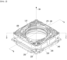
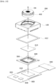
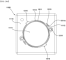
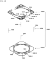
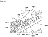
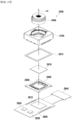
- FIG. 4a is a perspective view of a housing (140), a circuit substrate (190), a first position sensor (170) and a capacitor (195) illustrated in FIG. 1
- FIG. 4b is a coupled perspevtive view of a housing (140), a first magnet (130), a circuit substrate (190), a first position sensor (170) and a capacitor (195).
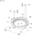
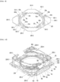
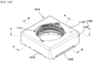
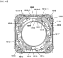
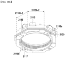
- the housing (140) may generally take a hollowed cylindrical shape.
- the housing (140) may be disposed with a polygonal (e.g., square, octagonal) or round opening, and the opening of the housing (140) may take a through hole shape passing through the housing (140) to the optical axis direction.
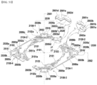
- the housing (140) may comprise a plurality of lateral portions (141-1 to 141-4) and corner portions (142-1 to 142-4).
- the housing (140) may comprise mutually-discrete first to fourth lateral portions (141-1 to 141-4) and first to fourth corner portions (142-1 to 142-4).
- first and second lateral portions (141-1, 141-2) of housing (140) may face each other or mutually be positioned at an opposite side
- third and fourth lateral portions (141-3, 141-4) of housing (140) may face each other or mutually be positioned at an opposite side.
- corner portions (142-1 to 142-4) may be disposed on the corner or edge of the housing (140).
- the number of lateral portions of housing (140) may be four (4), and the number of corner portions may be four (4), but the present invention is not limited thereto, and the number may be more than five (5).
- Each of the lateral portions (141-1 to 141-4) of housing (140) may be so disposed as to be parallel with any one corresponding lateral plates (302) of cover member (300).
- housing (140) may correspond to or face the first lateral portions (110b-1) of bobbin (110), and the corner portions (142-1 to 142-4) of housing (140) may correspond to or face the second lateral portions (110b-2) of bobbin (110).
- the corner portions (142-1 to 142-4) of housing (140) may be disposed or installed with a first magnet (130).
- corners or corner portions (142-1 to 142-4) of housing (140) may be disposed with an accommodation portion (141a) or acceptance portion for accommodating the magnet (130).
- the accommodation portion (141a) of housing (140) may be provided on at least one lower part or lower end of the corner portions (142-1 to 142-4) of housing (140).
- accommodation portion (141a) of housing (140) may be provided at a lower inner part or lower inner end of each of the four corner portions (142-1 to 142-4).
- the accommodation portion (141a) of housing (140) may be formed with a recess, for example, a concaved groove, having a shape corresponding to that of the first magnet (130), but the present invention is not limited thereto.
- a lateral surface of the accommodation portion (141a) of housing (140) facing the first coil (120) may be formed with a first opening
- a lower surface of the accommodation portion (141a) of housing (140) facing the second coil (230) may be formed with a second opening, which is intended to facilitate an easy installation of first magnet (130).
- a first surface (11a) of the first magnet (130) fixed to or disposed on the accommodation portion (141a) of housing (140) may be exposed through the first opening of the accommodation portion (141a).
- a lower surface (11a) of the first magnet (130) fixed to or disposed on the accommodation portion (141a) of housing (140) may be exposed through the second opening of the accommodation portion (141a).
- the housing (140) may be disposed with an escape recess (41) provided on an upper surface of the corner portions (142-1 to 142-4) in order to avoid a spatial interference with the first frame connection part (153) of the upper elastic member (150).
- the escape recess (41) of housing (140) may take a shape depressed from an upper surface of housing (140), and may be so disposed as to be more adjacent to a center of housing than to a stopper (145) or to an adhesive infusion hole (147).
- the escape recess (41) may be disposed at an inner lateral surface, which is a center direction of housing (140) based on the stopper (145) of housing (140), and an outer lateral surface, which is an opposite side, may be disposed with the adhesive infusion holes (146a, 146b).
- the corner portions (142-1 to 142-4) of housing (140) may be formed with a recess portion (25a) corresponding to or facing the protruder (115) of bobbin (110).
- the recess portion (25a) of housing (140) may be disposed on the accommodation portion (141a) of housing (140).
- the recess portion (25a) of housing (140) may be disposed on a floor surface of the escape recess (41).
- the floor surface of the recess portion (25a) may be so disposed as to be lower than the floor surface of escape recess (41), and the accommodation portion (141a) of housing (140) may be so disposed as to be lower than the floor surface of escape recess (41).
- the first magnet (130) may be fixed to the accommodation portion (141a) using an adhesive, but the present invention is not limited thereto.
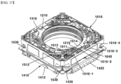
- the housing (140) may comprise an installation recess (14a, or accommodation groove) for accommodating a circuit substrate (190), an installation recess (14b, or accommodation groove) for accommodating a first position sensor (170), and an installation recess (14c, or accommodation grooove) for accommodating a capacitor (195).
- the installation recess (14a) of housing (140) may be provided on an upper surface or an upper end of at least any one (e.g., 141-1) of the lateral portions (141-1 to 141-4) of housing (140).
- the installation recess (14a) of housing (140) may have a shape that corresponds to or matches that of the circuit substrate (190).
- the capacitor (195) may be disposed or mounted on a first surface (19b) of circuit substrate (190).
- the capacitor (195) may take a chip shape and, at this time, the chip may comprise a first terminal corresponding to one end of the capacitor (195) and a second terminal corresponding to the other end of the capacitor (195).
- the capacitor (195) may be expressed by replacing with a "capacitive element” or a condenser.
- the capacitor (195) may be electrically connected in parallel to the first and second terminals (B1, B2) for providing a power (or a driving signal) to the position sensor (170) from outside.
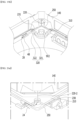
- corner portions (142-1 to 142-4) of housing (140) may be disposed with support members (220-1 to 220-4).
- the diameter of hole (147) may take a shape of gradually increasing in size to a lower surface direction from an upper surface of housing (140), but the present invention is not limited thereto, and in any other exemplary embodiments, the diameter of the hole (147) may be constant.
- An outer lateral surface (148) of the corner portions (142-1 to 142-4) may be provided with an escape recess (148a) in order to form a path through which the support members (220-1 to 220-4) can pass and to avoid a spatial interference between the support members (220-1 to 220-4) and the corner portions (142-1 to 142-4) of housing (140).
- the escape recess (148a) may be connected to the hole (147) of housing (140), and may take a semi-sphere shape or a semi-oval shape. However, the present invention is not limited thereto.
- the escape recess (148a) may be connected at a lower surface or a lower end thereof to a lower surface of the housing (140).
- the stopper (145) may be disposed on an upper surface of each of the corner portions (142-1 to 142-4) of housing (140), but the present invention is not limited thereto, and in any other exemplary embodiments, the stopper (145) may be disposed at a lateral surface of the housing (140).
- a corner of an upper surface of corner portions (142-1 to 142-4) of housing (140) may be provided with a guide protruder (146) to prevent the damper from overflowing.
- At least one first coupling part (143) coupled with the first outer lateral frame (152) of the upper elastic member (150) may be disposed at an upper surface, an upper end or an upper lateral part of the housing (140).
- the first coupling part (143) of housing (140) may be disposed on at least one of lateral portions (141-1 to 141-4) of housing (140) or corner portions (142-1 to 142-4).
- a lower surface, a lower end or a lower lateral part of the housing (140) may be formed with a second coupling part (149) coupled or fixed to a second outer lateral frame (162) of lower elastic member (160).
- each of the first and second coupling parts (143, 149) of housing (140) may take a protrusion shape, but the present invention is not limited thereto, and in other exemplary embodiments, each of the first and second coupling parts (143, 149) of housing (140) may take a groove or plane surface shape.
- first coupling part (143) of housing (140) and the hole (152a) of the first outer lateral frame (152) of upper elastic member (150) may be coupled
- second coupling part (149) of housing (140) and the hole (162a) of second outer lateral frame (162) of lower elastic member (160) may be coupled using an adhesive or thermal fusion.
- An escape recess (44a) may be disposed on a lower surface of at least one of the lateral portions (141-1) of housing (140) in order to avoid a spatial interference with an area where the second outer lateral frame (162-1 to 162-3) of lower elastic member (160) and the second frame connection part (163) meet.
- the first magnet (130) may be disposed on at least one of the corners ⁇ or corner portions (142-1 to 142-4) ⁇ of housing (140).
- the first magnet (130) may be disposed on each of the corners of housing (140).
- the first magnet (130) at an initial position of AF mover may be so disposed on the housing (140) as to allow being partially overlapped with the first coil (120) to a direction parallel with a straight line that is perpendicular to the optical axis and that passes the optical axis.
- the first magnet (130) may be inserted into or disposed in an inner lateral surface of any one corresponding accommodation portion (141a) in the corner portions (141-1 or 141-4).
- the first magnet (130) may take a polygonal shape that is easy to be accommodated with the corner portions of the housing (140).
- first surface (11a) of the first magnet (130) may be greater than that of second surface (11b).
- first surface (11a) of first magnet (130) may be a surface facing any one surface ⁇ or an outer lateral surface of bobbin (110) ⁇ of first coil (120), and the second surface (11b) may be an opposite surface of the first surface (11a).
- a crosswise direction of second surface (11b) of first magnet (130) may be a direction perpendidcular to a direction facing an upper surface from a lower surface of first magnet (130) at the second surface (11b) of the first magnet (130), or a direction perpendicular to an optical axis direction from the second surface (11b) of the first magnet (130).
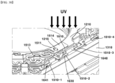
- FIG.7a is an enlarged view of a circuit substrate (190) and a first position sensor (170)
- FIG. 7b is a block diagram of a first position sensor (170) illustrated in FIG. 7a according to an exemplary embodiment of the present invention.
- the first terminal (B1) of circuit substrate (190) may be disposed on the first extension region (A1) of body part (S1) of the circuit substrate (190), and the second terminal (B2) may be disposed on the second extension region (A2) of body part (S1) of circuit substrate (190).
- the circuit substrate (190) may comprise a groove (8a) or a hole provided between the fifth terminal (B5) and the sixth terminal (B6).
- the groove (8a) may take a shape depressed from a lower surface of the circuit substrate (190), and may be all opened to the first surface (19b) and the second surface (19a) of circuit substrate (190).
- At least one of the fifth terminal (B5) and the sixth terminal (B6) may comprise a groove (7a) or a via formed at a lower surface of the circuit substrate (190).
- the fifth terminal (B5) and the sixth terminal (B6) may comprise a curved portion depressed from a lower surface of the circuit substrate (190), e.g., a semi-circular via, or a groove.
- a contacted area between the fifth terminal (B5) and the sixth terminal (B6) may be increased by the groove (7b) to thereby improve the adhesion and solderability.
- the circuit substrate (190) may comprise a groove (or recess 90a) interposed between the second terminal (B2) and the third terminal (B3), and a groove (or recess 90b) interposed between the first terminal (B1) and the fourth terminal (B4).
- the groove (90a, 90b) may be expressed by being replaced with an "escape groove”.
- the circuit substrate (190) may comprise a circuit pattern or a wiring (not shown) for electrically connecting the first to sixth terminals (B1 to B6) and the first position sensor (170).
- the first position sensor (170) may detect a magnetic field or magnetic strength of second magnet (180) installed on the bobbin (110) in response to the motion of bobbin (110), and may output an output signal in response to the detected result.
- the first position sensor (170) may be disposed on a first surface (19b) of circuit substrate (190). In another exemplary embodiment, the first position sensor (170) may be disposed on the second surface (19a) of the circuit substrate (190).
- the first position sensor (170) may comprise a Hall sensor (61) and a driver (62).
- the Hall sensor (61) may be formed with silicone series, and an output (VH) of the Hall sensor (61) may be increased as the surrounding (ambient) temperature increases.
- the surrounding temperature may be a temperature of lens driving device, e.g., a temperatue of circuit substrate (190), a temperature of Hall sensor (61), or a temperature of driver (62).
- the Hall sensor (61) may be formed with GaAs, and an output (VH) of the Hall sensor (61) may decrease relative to the surrounding temperature.
- the output of the Hall sensor (61) may have an approximate -0.06%/°C inclination relative to the surrounding temperature.
- the first position sensor (170) may further comprise a temperature sensing element (63) configured to detect a surrounding temperature.
- the temperature sensing element (63) may output, to the driver (62), a temperature detection signal (Ts) based on a result of measuring a temperature around the first position sensor (170).
- the Hall sensor (61) of first position sensor (190) may generate an output (VH) in response to a result of detecting the magnetic strength of second magnet (180).
- the size of output of the first position sensor (190) may be proportionate to the magnetic strength of the second magnet (180).
- the driver (62) may output a driving signal (dV) for driving the Hall sensor (61), and a driving signal (Id1) for driving the first coil (120).
- the driver (62) may receive a clock signal (SCL), a data signal (SDA) and power signals (VDD, GND) from the controller (830, 780) using the data communication using protocol, for example, using I2C communication.
- SCL clock signal
- SDA data signal
- VDD power signals
- GND power signals
- a first power signal may be a ground voltage, or 0[V]
- a second power signal may be a preset voltage for driving the driver (62) and may be a DC voltage and/or an AC voltage, but the present invention is not limited thereto.
- the driver (62) may generate a driving signal (dV) for driving the Hall sensor (61) using the clock signal (SCL) and the power signals (VDD, GND), and a driving signal (Id1) for driving the first coil (120).
- the first position sensor (170) may comprise four (4) terminals for transmitting and receiving a clock signal (SCL), a data signal (SDA) and power signals (VDD, GND), and two (2) terminals for providing a driving signal to the first coil (120).
- the driver (62) may receive the output (VH) of Hall sensor (61), and may transmit, to the controller (830, 780), a clock signal (SCL) on the output (VH) of Hall sensor (61) and a data signal (SDA) using the data communication using protocol, e.g., using I2C communication.
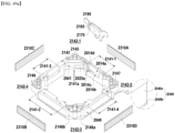
- the upper elastic member (150) may be coupled to an upper part, an upper surface or an upper end of bobbin (110), and the lower elastic member (160) may be coupled to a lower part, a lower end or a lower surface of bobbin (110).
- each of the plurality of upper elastic units may be disposed on the first lateral portion (141-1) of housing (140) disposed with the circuit substrate (190), and at least one upper elastic unit may be disposed on each of the remaining second to fourth lateral portions (141-2 to 141-4) less the first lateral portion (141-1) of housing (140).
- At least one of the first to fourth upper elastic units (150-1 to 150-4) may further comprise a first inner lateral frame (151) coupled with the bobbin (110), and a first frame connection part (153) connecting the first inner lateral frame (151) and the first outer lateral frame (152).
- each of the first and second upper elastic units (150-1, 150-2) may be disposed only with the first outer lateral frame, and may not be disposed with the first inner lateral frame and the first frame connection part, and each of the first and second upper elastic units (150-1, 150-2) may be spaced apart from the bobbin (110).
- Each of the third and fourth upper elastic units (150-3, 150-4) may comprise a first inner lateral frame (151), a first outer lateral frame and a first frame connection part (153), but the present invention is not limited thereto.
- the first inner lateral frame (151) of the third and fourth upper elastic units (150-3, 150-4) may be provided with a hole (151a) for being coupled with the first coupling portion (113) of bobbin (110), but the present invention is not limited thereto.
- a hole (152a) of the first inner lateral frame (151) may have at least one cut-out portion (51a) for allowing an adhesive member to be introduced between the first coupling portion (113) of bobbin (110) and the hole (151a).
- the first outer lateral frame (152) of the first to fourth upper elastic members (150-1 to 150-4) may be provided with a hole (152a) for being coupled with the first coupling portion (143) of housing (140).
- Each first outer lateral frame (151) of first to fourth upper elastic units (150-1 to 150-4) may incude a body part coupled with the housing (140) and connection terminals (P1 to P4) connected to any corresponding one of the first to fourth terminals (B1 to B4) of the circuit substrate (190).
- the connection terminals (P1 to P4) may be expressed by replacing the same with a "extension part”.
- the support member (220) may be coupled with the body part of the first outer lateral frame (151).
- Each first outer lateral frame of first to fourth upper elastic units (150-1 to 150-4) may comprise a first coupling portion (520) coupled to the housing (140), a second coupling portion (510) coupled to any corresponding one of the support members (220-1 to 220-4), a connection portion (530) connecting the first coupling portion (520) and the second coupling portion (510), and extension portions (P1 to P4) coupled to the second coupling portion (510) and extended to the first lateral portion (141-1) of the housing (140).
- Each body part of first to fourth upper elastic units (150-1 to 150-4) may comprise a first coupling portion (520). Furthermore, each body part of first to fourth upper elastic units (150-1 to 150-4) may further comprise at least one of a second coupling portion (510) and a connection portion (530).
- the second coupling portion (510) may be disposed with a hole (52) through which the support member (220-1 to 220-4) passes.
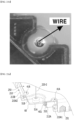
- One end of the support member (220-1 to 220-4) that has passed through the hole (52) may be directly coupled to the second coupling portion (510) by the conductive adhesive member or a solder (901, See FIG. 10 ), and the second coupling portion (510) and the support member (220-1 to 220-4) may be electically connected.
- the second coupling portion (510) is a region where the solder (901) is disposed for being coupled with the support member (220-1 to 220-4), and may comprise a hole (52) and a region about the hole (52).
- the first coupling portion (520) may comprise at least one coupling region (e.g., 5a, 5b) coupled with the housing (140) ⁇ e.g., corner portions (142-1 to 142-4) ⁇ .
- the coupling region (e.g., 5a, 5b) of first coupling portion (520) may comprise at least one hole (152a) coupled with the first coupling portion (143) of housing (140).
- each of the coupling regions (5a, 5b) may comprise at least one or more holes, and the corner portions (142-1 to 142-4) of housing (140) may be provided with one or more first coupling portions corresponding thereto.
- first coupling portion (520) of first to fourth upper elastic units (150-1 to 150-4) may be bilaterally symmetrical based on a baseline (e.g., 501, 502) in order to support the housing (140) in a balanced way for avoiding being biased to one side, but the present invention is not limited thereto.
- first coupling portions (143) of housing (140) may be bilaterally symmetrical based on a baseline (e.g., 501, 502), and two first coupling portions may be provided on both sides based on the baseline but the number is not limited thereto.
- the baseline (501, 502) may be a straight line that passes a center point (101) and any one corner of corners of corner portions (142-1 to 142-4) of housing (140).
- the baseline (501, 502) may a straight line that passes the center point (101) and mutually faces two corners among corners of corner portions (142-1 to 142-4) of housing (140) to a diagonal direction of the housing (140).
- Each of the first and second connection portions (530a, 530b) may comprise a bent portion that folds at least once or a curved portion that bends at least once, but the present invention is not limited thereto, and in another exemplary embodiment, each of the first and second connection portions (530a, 530b) may instead comprise a shape of a straight portion.
- Width of connection portion (530) may be smaller than that of the first coupling portion (520). Furthermore, the width of connection portion (530) may be smaller than width (or diameter) of the first coupling portion. In another exemplary embodiment, width of connection portion (530) may be the same as that of the first coupling portion (520), and may be same as the width (or diameter) of the first coupling portion.
- the first coupling portion (520) may be brought onto contact with an upper surface of the corner portions (142-1 to 142-4) of housing (140) and may be supported by the corner portions (142-1 to 142-4) of housing (140).
- the connection portion (530) may not be supported by the upper surface of housing (140), and may be spaced apart from the housing (140).
- a damper (not shown) may be filled in an empty space between the connection portion (530) and the housing (140).
- Each of the first and second extension portions (P1, P2) of first outer lateral frame of first and second upper elastic units (150-1, 150-2) may be extended from the first coupling portion (520, e.g., the first coupling region 5a) toward any corresponding one of the first and second terminals (B1, B2) of circuit substrate (190) disposed on the first lateral portion (141-1) of housing (140).
- first coupling portion (520) of the fourth upper elastic unit (150-4) may further comprise at least one coupling region (6c, 6d) connected to at least one of the third lateral portion (141-3) of housing (140) and the first corner portion (142-1).
- Each of the third and fourth extension portions (P3, P4) of the first outer lateral frame of third and fourth upper elastid units (150-3, 150-4) may be extended from the first coupling portion (520, e.g., the coupling region 6b, 6d) toward any corresponding one of the third and fourth terminals (B3, B4) of circuit substrate (190) disposed on the first lateral portion (141-1) of housing (140).
- the third and fourth extension portions (P3, P4) may comprise a portion that is folded or bent in order to allow an easy coupling with any corresponding one of the third and fourth terminals (B3, B4) of circuit substrate (190).
- the first outer lateral frame of the third upper elastic unit (150-3) may be connected between the first coupling portion (520) and the extension portion (P3), and may further comprise a first extension frame (154-1) disposed on the fourth lateral portion (141-4) of housing (140) and the second corner portion (142-2).
- the second extension frame (154-2) may comprise at least one coupling region (6c, 6d) coupled with the housing (140), where the coupling region (6c, 6d) may comprise a hole for being coupled with the first coupling portion (143) of housing (140).
- each of the first to fourth upper elastic units may comprise extension portions (P1 to P4) disposed on the first lateral portion (141-1) of housing (140), and as a result, the upper elastic units (150-1 to 150-4) may be easily coupled to the first to fourth terminals (B1 to B4) provided on the body part (S1) of circuit substrate (190) by the extension portions (P1 to P4).
- the first lateral portion (141-1) of housing (140) may be partially disposed with each of the first outer lateral frame (151) of first to fourth upper elastic units (150-1 to 150-4).
- Each of the upper elastic units (150-1 to 150-4) may be disposed or coupled to any corresponding one of the corner portions (142-1 to 142-4) of housing (140), and may comprise extension portions (P1 to P4) extended to the first lateral portion (141-1) of housing (140).
- the third extension portion (P3) of third upper elastic unit (150-3) may be extended toward the third terminal (B3) of the circuit substrate (190) by passing through the first recess (90a) of circuit substrate (190), and may be bent at least twice.
- fourth extension portion (P4) of fourth upper elastic unit (150-4) may be extended toward the fourth terminal (B4) of the circuit substrate (190) by passing through the second recess (90b) of circuit substrate (190), and may be bent at least twice.
- the second portion (1b) of the third extension portion (P3) (or third connection terminal) may be bent from the first portion (1a), and the third portion (1c) may be bent from the second portion (1b).
- the second portion (1b) of third extension portion (P3) may be interposed between the first bent region (2a) and the second bent region (2b) and can connect the first and second bent regions (2a, 2b).
- each of the first and third portions (1a, 1c) of third extension portion (P3) may be extended from the second corner portion (142-2) of housing (140) to a direction toward the first corner portion (141-1).
- the second portion (1b) of third extension portion (P3) may be extended from an inner surface of housing (140) to a direction toward the outer lateral surface.
- a part (e.g., the second portion 1b) of the third extension portion (P3) of third upper elastic unit (150-3) may be disposed within the first recess (90a) of circuit substrate (190) or may pass through the first recess (90a).
- the fourth extension portion (P4) of fourth upper elastic unit (150-4) may comprise a fourth portion (1d) extended from the first coupling portion (520, e.g., a coupled region 6d) of fourth upper elastic unit (150-4), a third bent region (2c or "a third bent portion") bent from the fourth portion (1d), a fifth portion (1e) extended from the third bent region (2c), a fourth bent region (2d or "a fourth bent portion”) bent from the fifth portion (1e), and a sixth portion (1f) extended from the fourth bent region (2d) toward a fourth terminal (B4) direction.
- the fifth portion (1e) of fourth extension portion (P4) may be disposed between the third bent region (2c) and the fourth bent region (2d), and may connect the third and fourth bent regions (2c, 2d).
- each of the first and second lower elastic units (160-1, 160-2) may comprise a second inner frame (161) coupled or fixed to a lower surface, a lower part or a lower end of bobbin (110), a second outer lateral frame (162-1 to 162-3) coupled or fixed to a lower surface, a lower part or a lower end of housing (140), and a second frame connection portion (163) mutually connecting the second inner frame (161) and the second outer lateral frame (162-1 to 162-3).
- the second inner frame (161) may be provided with a hole (161a) for being coupled with the second coupling portion (117) of bobbin (110), and the second outer lateral frame (162-1 to 162-3) may be provided with a hole (162a) for being coupled with the second coupling portion (149) of housing.
- connection frames (164-1, 164-2) may be disposed outside of the coil units (230-1 to 230-4) and magnets (130-1 to 130-4) based on the coil units (230-1 to 230-4) and magnets (130-1 to 130-4) in order to avoid a spatial interference with the second coil (230) and the first magnet (130).
- the outside of the coil units (230-1 to 230-4) and magnets (130-1 to 130-4) may be an opposite side of a region where a center of bobbin (110) or a center of housing (140) is situated based on the coil units (230-1 to 230-4) and magnets (130-1 to 130-4).
- connection frames (164-1, 164-2) may be so positioned as not to overlap the coil units (230-1 to 230-4) or/and magnets (130-1 to 130-4) to an optical axis direction, but the present invention is not limited thereto, and in another exemplary embodiment, at least parts of the connection frames (164-1, 164-2) may be aligned or overlapped with the coil units (230-1 to 230-4) or/and magnets (130-1 to 130-4) to an optical axis direction.
- the support members (220-1 to 220-4) may be spaced apart from the housing (140), and may not be fixed to the housing (140), where one end of the support members (220-1 to 220-4) may be directly connected or coupled to a second coupling portion (510) of upper elastic units (150-1 to 150-4). Furthermore, the other end of the support members (220-1 to 220-4) may be directly connected or coupled to the circuit substrate (250).
- the support members (220-1 to 220-4) may pass through a hole (147) provided on the corner portions (142-1 to 142-4) of housing (140), but the present invention is not limited thereto.
- the support members may be adjacently disposed to a boundary line between the lateral portions (141-1 to 141-4) of housing (140) and corner portions (142-1 to 142-4), and may not pass through the corner portions (142-1 to 142-4) of housing (140).
- the first support member (220-1) may be disposed on a first corner portion (142-1) of housing (140), and may be coupled to the second coupling portion (510) of the first upper elastic unit (150-1).
- the fourth support member (220-4) may be disposed on the fourth corner portion (142-4) of housing (140) and may be coupled to the second coupling portion (510) of the fourth upper elastic unit (150-4).
- power signals may be provided to the first and second support members (220-1, 220-2) through the first and second terminals (251-1, 251-2) of circuit substrate (250).
- power signals (VDD, GND) may be provided to the first and second terminals (B1, B2) of circuit substrate (190) through the first and second support members (220-1, 220-2) and the first and second upper elastic units (150-1, 150-2).
- the first position sensor (170) may receive the power signals (VDD, GND) through the first and second terminals (B1, B2) of circuit substrate (190).
- the first terminal (B1) of circuit substrate (190) may be any one terminal of the VDD terminal and GND terminal
- the second terminal (B2) of circuit substrate (190) may be any one remaining terminal of the VDD terminal and GND terminal.
- the third and fourth support members (220-3, 220-4) may be provided with a clock signl (SCL) and a data signal (SDA) through the third and fourth terminals (251-3 to 251-4) of circuit substrate (250).
- SCL clock signl
- SDA data signal
- the third and fourth terminals (B3, B4) of circuit substrate (190) may be provided with a clock signal (SCL) and a data signal (SDA) through the third and fourth support members (220-3,220-4) and the third and fourth upper elastic units (150-3, 150-4).
- SCL clock signal
- SDA data signal
- the first position sensor (170) may receive a clock signl (SCL) and a data signal (SDA) through the third and fourth terminals (B3, B4) of circuit substrate (190).
- SCL clock signl
- SDA data signal
- the first position sensor (170) may be provided with a power signal (VDD) through the first terminal (251-1) of circuit substrate (250), a first support member (220-1), a first upper elastic unit (150-1), and a first terminal (B1) of circuit substrate (190).
- VDD power signal
- the first position sensor (170) may be provided with a power signal (GND) through the second terminal (251-2) of circuit substrate (250), a second support member (220-2), a second upper elastic unit (150-2), and a second terminal (B2) of circuit substrate (190).
- GND power signal
- the first position sensor (170) may be provided with a clock signal (SCL) through the third terminal (251-3) of circuit substrate (250), a third support member (220-3), a third upper elastic unit (150-3), and a third terminal (B3) of circuit substrate (190).
- SCL clock signal
- Each of the fifth and sixth terminals (B5, B6) of circuit substrate (190) may be connected or coupled to any corresponding one of second outer lateral frame (162-1) of the first and second lower elastic units (160-1, 160-2).
- the second outer lateral frame (162-1) of first lower elastic unit (160-1) may be disposed with a first bonding portion (81a) for being coupled with the fifth terminal (B5) of circuit substrate (190) using a solder or a conductive adhesive member.
- the second outer lateral frame (162-1) of second lower elastic unit (160-2) may be disposed with a second bonding portion (81b) for being coupled with the sixth terminal (B6) of circuit substrate (190) using a solder or a conductive adhesive member.
- each of the first and second holes (82a, 82b) can pass through the second outer lateral frame (161-1), and may have an opening that is opened to one lateral surface of the second outer lateral frame (161-1), and the present invention is not limited thereto, and in another exemplary embodiment, each of the first and second holes (82a, 82b) may not have an opening that is opened to one lateral surface of the second outer lateral frame (161-1).
- the housing (140) may comprise a recess (31) depressed from a lower surface of first lateral portion (141-1).
- a floor surface of the recess (31) of the housing (140) may have a staircase (step) with a lower surface of housing (140) to an optical axis direction.
- the floor surface of the recess (31) of the housing (140) may be so disposed as to be higher than a lower surface of housing (140).
- the recess (31) of housing (140) may be overlapped with the recesses (82a, 82b) of second outer lateral frame (162-1) of the first and second lower elastic units (160-1, 160-2) to an optical axis direction, but the present invention is not limited thereto and in another exemplary embodiment, both recesses may not be overlapped.
- a lower surface (11c) of first magnet (130) disposed on the accommodation portion (141a) of housing (140) may be so positioned as to be lower than a lower surface of the second outer lateral frame (162-1 to 162-3) of first and second lower elastic units (160-1, 160-2), but the present invention is not limited thereto, and in another exemplary embodiment, the lower surface (11c) of first magnet (130) may be higher than or same in height as the lower surface of the second outer lateral frame (162-1 to 162-3) or the lower surface of housing (140).
- the other end of the support member (220) may be coupled with the circuit substrate (250, or circuit member 231) at a position lower than the lower surface (11c) of the first magnet (130).
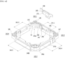
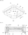
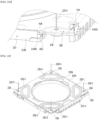
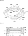
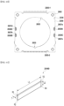
- the base (210) may be disposed with an opening (C3) corresponding to an opening of bobbin (110), or/and an opening of housing, and may take a shape corresponding to or matching to that of a cover member (300), e.g., a square shape.
- the opening (C3) of base (210) may take a through hole shape that passes through the base (210) to an optical axis direction.
- the pads (27a to 27d) of circuit substrate (250) may be disposed or formed on a lower surface of circuit substrate (250) adjacent to at least one lateral surface of ciruit substrate (250) not formed with the terminal surface (253).
- the coil units (230-1 to 230-4) may be omitted from the circuit member (231), and instead may be embodied with coil blocks of a ring shape.
- the coil units (230-1 to 230-4) may be embodied with a circuit pattern shape directly formed on the circuit substrate (250), e.g., an FP coil shape.
- the circuit substrate (250) may be expressed by being replaced with a "circuit member”, and the circuit member may be disposed with a substrate portion formed with the coil units (230-1 to 230-4) and a terminal portion formed with terminals, and explanation on the substrate portion may be applied or applied mutatis mutandis with that of circuit substrate (250), and explanation on the terminal portion may be applied or applied mutatis mutandis with that of terminal portions (253, 253-1, 253-2) of circuit substrate (250).
- At least one of the circuit member (231) or/and the circuit substrate (250) may be formed with a hole or an escape recess to avoid a spatial interference with the support member (220).
- the circuit member (231) may be provided with an escape recess (24) to avoid a spatial interference with the fifth and sixth terminals (B5, B6) of circuit substrate (190).
- the escape recess (24) may be formed on any one side of circuit member (231) to correspond to or face or overlap with the fifth and sixth terminals (B5, B6) of circuit substrate (190) to an optical axis direction.
- the escape recess (24) may be interposed between the first coil unit (230-1) and the fourth coil unit (230-4).
- circuit substrate (250) and the circuit member (231) are expressed by being divided as separate elements, the present invention is not limited thereto, and in another exemplary embodiment, the circuit substrate (250) and the circuit member (231) may be also collectively expressed by a term of "circuit member” or "substrate". In this case, the other end of support members may be coupled to the "circuit member (e.g., a lower surface of circuit member)".
- Each of the OIS position sensors (240a, 240b) may detect the magnetic field strength of magnets (130-1 to 130-4) in response to motion of OIS mover to a direction perpendicular to an optical axis and may output an output signal in response to a detected result.
- the displacement of OIS mover may be detected using the output signal of each of the OIS position sensors (240a, 240b), and a controller (830, 780) may perform the OIS feedback operation using the output signals of the OIS position sensors (240a, 240b).
- the first OIS position sensor (240a) may be overlapped with a first straight line that connects a first corner of circuit substrate (250) with a center of opening (C2) of circuit substrate (250).
- the second OIS position sensor (240b) may be overlapped with a second straight line that connects a second corner of circuit substrate (250) with a center of opening (C2) of circuit substrate (250).
- first OIS position sensor (240a) may be aligned or overlapped with the first straight line
- second OIS position sensor (240b) may be aligned or overlapped with the second straight line.
- the first straight line and the second straight line may be mutually perpendicular.
- the terminal surface (253) of circuit substrate (250) may be provided with terminals (251-1 to 251-n).
- Signals (SCL, SDA, VDD, GND) for data communication with the first position sensor (190) may be transmitted or received through a plurality of terminals (251-1 to 251-n) disposed on the terminal surface (253) of circuit substrate (250), and may supply a driving signal to the OIS position sensors (240a, 240b), and may receive signals outputted from the OIS position sensors (240a, 240b) and output the same to an outside.
- the circuit substrate (250) may comprise a hole (250a) through which the support members (220-1 to 220-4) can pass.
- the number and position of hole (250a) may correspond or match to those of the support members (220-1 to 220-4).
- the hole (250a) may be adjacently formed to a corner of circuit substrate (250) in reponse to each of the support members (220-1 to 220-4), and may correspond to or face the escape recess (23) of circuit member (231) to an optical axis direction.
- the support members (220-1 to 220-4) may connect the upper elastic units (150-1 to 150-4) and the circuit member (231), and may electrically connect the upper elastic units (150-1 to 150-4) and the circuit member (231), and the support members (220-1 to 220-4) may be electically connected with the circuit substrate (250) through the circuit member (231).
- the exemplary embodiment shows a structure where a driving signal is directly provided to the first coil (120) from the first position sensor (170), the number of support members may be reduced and an electrical connecting structure is simplified, compared with a case where a driving signal is directly provided to the first coil (120) through the circuit substrate (250).
- the first position sensor (170) can be embodied by a driver IC configured to measure temperatures
- output of Hall sensor is made to be compensated to allow having a minimum change in response to temperature changes, or the output of Hall sensor is made to be compensated to allow having a constant inclination in response to temperature changes, whereby accuracy of AF driving can be improved regardless of temperature changes.
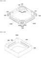
- the cover member (300) may take a box shape with a lower surface opened, and comprising an upper plate (301) and lateral plate (302), and the lower surface (e.g., a lower surface of lateral plate 302) of cover member (300) may be coupled with a base (210) ⁇ e.g., staircase (211) or/and escape portions (212-1 to 212-4) ⁇ .
- the upper plate (301) of cover member (300) may take a round, or polygonal (e.g., square or octagonal) shape, but the present invention is not limited thereto.
- the cover member (300) may comprise an opening on the upper plate (301) for exposing a lens (not shown) coupled with the bobbin (110) to an ouside light.
- the material of cover member (300) may be of a non-magnetic substance such as SUS to prevent being attached with the first magnet (130), but the cover member (300) may function as a yoke for improving the electromagnetic force between the first coil (120) and a first magnet (130) by forming with a magnetic material.
- the following structure may be provided.
- the first and second terminals (B1, B2) of circuit substrate (190) for allowing being provided with the power signals (GND, VDD) may be electrically connected to the first and second support members (220-1, 220-1) disposed on two corner portions (142-1, 142-2) adjacent to the first lateral portion (141-1) of housing (140) disposed with the first position sensor (170), whereby the path can be shortened.
- the path may be shortened by allowing the first and second terminals (B1, B2) of circuit substrate (190) to be disposed on the body part (S1) of circuit substrate (190).
- the first terminal (B1) is disposed at one end of the circuit substrate (190) to allow the first terminal (B1) of circuit substrate (190) to be overlapped with the first corner portion (142-1) of housing (140) to an optical axis direction
- the second terminal (B2) is disposed at the other end of the circuit substrate (190) to allow the second terminal (B2) of circuit substrate (190) to be overlapped with the second corner portion (142-2) of housing (140) to an optical axis direction, whereby the path can be shortened.
- a discrete distance (e.g., shortest discrete distance) between the first terminal (B1) of circuit substrate (190) and the first support member (220-1) may be shorter than a discrete distance (e.g., shortest discrete distance) between the third terminal (B3) of circuit substrate (190) and the first support member (220-1) and a discrete distance (e.g., shortest discrete distance) between the fourth terminal (B4) of circuit substance (190) and the first support member (220-1).
- a discrete distance (e.g., shortest discrete distance) between the second terminal (B2) of circuit substrate (190) and the second support member (220-2) may be shorter than a discrete distance (e.g., shortest discrete distance) between the third terminal (B3) of circuit substrate (190) and the second support member (220-2) and a discrete distance (e.g., shortest discrete distance) between the fourth terminal (B4) of circuit substance (190) and the second support member (220-2).
- Each length of the first and second extension portions (P1, P2) can be shortened by the shortened path because of the abovementioned reasons, whereby resistance ⁇ e.g., resistance of first and second upper elastic units (150-1, 150-2) ⁇ of path can be reducerd.
- each of the first upper elastic unit (150-1) connected to the first terminal (B1) of circuit substrate (190) and the second upper elastic unit (150-2) connected to the second terminal (B2) is disposed with a first outer lateral frame coupled with the housing (140), the first inner frame (151) and the first frame connection portion are not disposed, such that resistance can be reduced compared with the second and fourth upper elastid units (150-3, 150-4).
- each of the third upper elastic unit (150-3) and the fourth upper elastic unit (150-3) ⁇ e.g., third extension portion (P3) or fourth extension portion (P4) ⁇ may be coupled to the third and fourth terminals (B3, B4) through the circuit substrate (190).
- the exemplary embodiment can reduce the number of support members, and the size of lens driving device can be also reduced by the reduced number of support members.
- thickness of support members may be increased in order to obtain the same elasticity instead of reducing the number of support members, and as the thickness of support members is increased, the influence of the OIS mover being received by the external shock can be decreased.
- the escape recess (17) may prevent the solder (39A), the circuit substrate (250), or/and the base (210) from being damaged by soldering while the spatial interference between solders (39A) formed at a lower surface of circuit substrate (250) and the upper surface of base (210) is avoided.
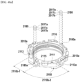
- a diameter (R) of base (210) may gradually increase from a center of base (210) to a direction (203) toward an imaginary corner (203) of base (210).
- the escape portion (e.g., 212-2) of base (210) in FIG. 18a takes a recess type having a curved or bent shape
- the present invention is not limited thereto, and the escape portion may be sufficient in shape if the shape is adequate to avoid the support member (220), and is adequate to be coupled to an inner surface of a corner of the cover member (300) by the adhesive member (290).
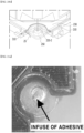
- the recess (310) of base (210) may function to restrict or prevent introduction of adhesive member (290) toward one end of support member (220) that has passed through a hole (250a) of circuit substrate (250).
- the recess (310) of base (210) may take a shape, e.g., a recess or a groove, depressed from an upper surface (210A) of base (210).
- the upper surface (210A) of base (210) may be a surface corresponding to or facing a lower surface of circuit substrate (250) to an optical axis direction.
- the upper surface (210A) of base (210) may be a surface that contacts a lower surface of circuit substrate (250).
- the recess (310) of base (210) may be spaced apart from an outer lateral surface (311) of corner portion (11) of base (210) formed by an escape portion (212-2).
- the floor surface (10A) may be so formed as to be lower than the upper surface (210A) of base (210).
- the height of floor surface (10A) may be so formed as to be higher than that of the upper surface (210A) of base (210) based on a lower surface (210B) of base (210).
- one end of recess (310) may be opened to any one outer lateral surface (213A) of base (210) adj acent to the escape portion (212-2).
- the other end of recess (310) may be opened to the other outer lateral surface (213B) of base (210) adjacent to the escape portion (212-2).
- the recess (310) may comprise at least one of a first opening (HO1) opened to any one outer lateral surface (213A) of base (210) adj acent to the escape portion (212-2), and a second opening (HO2) opened to the other outer lateral surface (213B) of base (210) adjacent to the escape portion (212-2). This is to prevent the adhesive member (290) from escaping to an outside of base (210) through the first opening (HO1) and the second opening (HO2).
- a distance from one end ⁇ or first opening (HO1) ⁇ of recess (310) to the other end ⁇ or second opening (HO2) ⁇ of recess (310) may be greater than a width ⁇ or width of floor surface (10A) ⁇ of recess (310).
- the shape of recess (310) may correspond or match to that of the outer lateral surface (311) of corner portion of base (210) or to that of escape portion (212-2).
- the base (210) may be such that a partition (330) exists between the recess (310) and the escape portion (212-2).
- the partition (330) may function to restrict or prevent the adhesive member (290) from invading into a hole (250a) of circuit substrate (250).
- the recess (310) of base (210) may be disposed with or remained with some of adhesive member (290). But the present invention is not limited thereto. In another exemplary embodiment, the recess (310) of base (210) may not be disposed with or remained with some of adhesive member (290).
- a lower surface of corner portion of base (210) adjacent to the escape portion (212-1 to 212-4) may be formed with a staircase portion (320) having a step with a lower surface (210B) of base (210) to an optical axis direction.
- the staircase portion (320) may be expressed by being replaced with a "recess” or a "recess portion”.
- the staircase portion (320) may be formed at a lower surface of base (210) about the escape portion (212-1 to 212-4).
- the staircase portion (320) may be so formed as to wrap at least some areas of the escape portion (212-1 to 212-4).
- the staircase portion (320) may be interposed between a lower surface of base (210) and the adhesive member (290).
- the staircase portion (320) may comprise a first surface (321) having a step (H2) with the lower surface (210B) of base (210) to an optical axis direction, and a second surface (322) connecting the first surface (321) and the lower surface (210B) of base (210).
- the first surface (321) of staircase portion (320) may be so positioned as to be higher than a lower surface (210B) of base (210). For example, a distance to the first surface (321) of staircase portion (320) to an optical axis direction based on an upper surface (210A) of base (210) may be shorter than a distance to a lower surface (210B) of base (210) to an optical axis direction based on the upper surface (210A) of base (210).
- a distance ⁇ or depth (H1) of recess ⁇ from the upper surface (210A) of base (210) to the floor surface (10A) of recess (310) may be shorter than or the same as the step (H2) of staircase portion (320) (H1 ⁇ H2).
- the distance may be H1>H2.
- H2 is a height of a first surface (321) based on a lower surface of base (210).
- first surface (321) of staircase portion (320) may abut the escape portion (212-1 to 212-4).
- first surface (321) of staircase portion (320) may abut an outer lateral surface (311) of corner portion (11) of base (210) formed by the escape portion (212-2).
- the staircase portion (320) may be overlapped with the recess (310) of base (210) to an optical axis direction.
- one end of staircase portion (320) may abut any one outer lateral surface (213A) of base (210) adjacent to an escape portion (e.g., 212-2), and the other end of staircase portion (320) may abut the other end of outer lateral surface (213B) of base (210) adjacent to an escape portion (e.g., 212-2).
- the adhesive members (290-1 to 290-4) may be also coated on one region (e.g., first region) of a lower surface of base (210) adjacent to the escape portions (212-1 to 212-4) of base (210). Furthermore, for example, the adhesive members (290-1 to 290-4) may be also disposed on one region of inner lateral surface of lateral plates of cover member (300) adjacent to an inner surface of corners (305-1 to 305-4) of cover member (300).
- the second opening (HO2) of recess (310) of base (210) may be so disposed as to be nearer to the support member ⁇ 220, or the corner (60) of circuit substrate (250) ⁇ than to the second region (210A2) of upper surface (210A) of base (210).
- FIG. 23a shows a positional relationship between a recess (310) of a base (210) and a first recess (42A) of a circuit substrate (250) according to another exemplary embodiment
- FIG. 23b shows a positional relationship between a recess (310) of a base (210) and a second recess (42B) of a circuit substrate (250) according to another exemplary embodiment.
- the first recess (42A) of FIG. 23a may be a modification of the first recess (41A) of FIG. 22a
- the second recess (42B) of FIG. 23b may be a modification of second recess (41B) of FIG. 22b .
- each of the first recess (42A) and the second recess (42B) may take a semi-circular shape, a semi-oval shape or a curved shape, but the present invention is not limited thereto and may also take a polygonal shape.
- one part of the recess (310) of base (210) and the first recess (42A) of circuit substrate (250) may be mutually overlapped to an optical axis direction
- the other part of the recess (310) of base (210) and the second recess (42B) of circuit substrate (250) may be mutually overlapped to an optical axis direction.
- first recess (42A) may be disposed between the terminal portion (253) and a corner (60) of the circuit substrate (250), and the second recess (42B) may be disposed between the terminal (30A to 30D) of circuit substrare (250) and a corner of the circuit substrate (250),
- the adhesive member introduced into a first region (210A3) of upper surface (210A) of base (210) exposed by the first recess (42A) or/and a second region (210A4) of base (210) exposed by the second recess (42B) may be easily introduced into the recess (310) of base (210) and discharged or released outside of the base (210) to thereby improve the discharge effect of adhesive member.
- the lens driving device may be used to various fields, e.g., camera modules or optical apparatus.
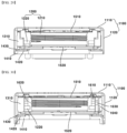
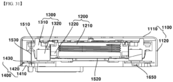
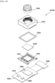
- FIG. 25 shows an exploded perspective view of a camera module (200) according to an exemplary embodiment of the present invention.
- the lens barrel (400) may be mounted on a bobbin (110) of lens driving device (100).
- the first holder (600) may be disposed underneath the base (210) of lens driving device (100).
- the filter (610) may be mounted on the first holder (600), and the first holder (600) may be disposed with a protruder (500) accommodated with the filter (610).
- the adhesive member (612) can couple or attach the base (210) of lens driving device (100) to the first holder (600).
- the adhesive member (612) may also function to prevent foreign objects from being introduced into the lens driving device (100), in addition to the abovementioned adhesive funection.
- the adhesive member (612) may be an epoxy, a thermosetting adhesive or a UV curable adhesive.
- the filter (610) may function to prevent a light of particular frequency bandwidth of lights that has passed the lens barrel (400) from being introduced into the image sensor (810).
- the filter (610) may be an infrared cut-off filter, but the present invention is not limited thereto. At this time, the filter (610) may be so disposed as to be parallel with an x-y plain surface.
- An area of the first holder (600) mounted with the filter (610) may be so formed with an opening as to allow the light having passed the filter (610) to be incident on the image sensor (810).
- the second holder (800) may be disposed at a lower surface of the first holder (600) and the second holder (600) may be disposed with an image sensor (810).
- the image sensor (810) is an area where an image comprising the incident light having passed the filter (610) is captured.
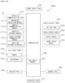
- the second holder (800) may be disposed with various circuits, elements, and controllers for transforming an image captured on the image sensor (810) to an electric signal and transmitting the same to an outside.
- the second holder (800) may be embodied by a circuit substrate mounted with an image sensor, formed with a circuit pattern and coupled with various elements.
- the first holder (600) may be expressed by being replaced with a "holder” or a "sensor base”, and the second holder (800) may be expressed by being replaced with a "substrate” or a "circuit substrate”.
- the image sensor (810) may receive an image comprised in a light incident on through the lens driving device (100), and may transform the received light to an electric signal.
- the filter (610) and the image sensor (810) may be so disposed as to be spaced apart by mutually facing each other to a first direction.
- the motion sensor (820) may be mounted on a second holder (800) and may be electrically connected with a controller (730) through a circuit pattern provided on the second holder (800).
- the controller (830) may be mounted on a second holder (800), and may be electrically connected to a second position sensor (240) of lens driving device (100) and a second coil (230).
- the second holder (800) may be electrically connected with a circuit substrate (250) of lens driving device (100), and the controller (830) mounted on the second holder (800) may be electrically connected to a second position sensor (240) of lens driving device (100) and a second coil (230) through the circuit substrate (250).
- the controller (830) may transmit a clock signal (SCL), a data signal (SDA) and power signals (VDD, GND) with the first position sensor (120) for I2C communication, and receive the clock signal (SCL) and the data signal (SDA) from the first position sensor (170).
- SCL clock signal
- SDA data signal
- VDD power signals
- GND power signals
- controller (830) may control a driving signal configured to perform an OIS operation on the OIS mover of lens driving device based on an output signal provided from the second position sensor (240) of the lens driving device (100).
- the connector (840) may be disposed with a port electrically connected to the second holder (800) for being electrically connected to an outside device.
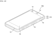
- the lens driving device (100) may be comprised in an optical apparatus with a purpose of improving an image of an object using light characteristics of reflection, refraction, absorption, interference, and diffraction, a purpose of increasing an eye vision, a purpose of recording and reproducing an image using a lens and a purpose of optical measurement, transmission or propagation of image.
- the optical apparatus may be a mobile phone, a portable phone, a smart phone, a portable smart device, a digital camera, a laptop computer, a digital broadcasting terminal, a PDA (Personal Digital Assistant), a PMP (Portable Multimedia Player), navigation and the like, but the present invention is not limited thereto, and may comprise any device configured to photograph an image or a photograph.
- a PDA Personal Digital Assistant
- PMP Portable Multimedia Player
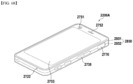
- FIG. 26 shows a perspective view of a portable terminal (200A) according to an exemplary embodiment of the present invention
- FIG. 27 is a block diagram of a portable terminal illusrtrated in FIG. 26 .
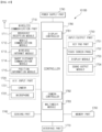
- a portable terminal (200A, hereinafter referred to as a "terminal") may comprise a body (850), a wireless communication part (710), an A/V input part (720), a sensing part (740), an input/output part (750), a memory part (760), an interface part (770), a controller (780) and a power supply part (790).
- Althogh the body (850) illustrated in FIG. 26 takes a bar shape
- the present invention is not limited thereto, and may be of various structures comprising a slide type structure where two or more sub-bodies are relatively movably coupled, a folder type structure, a swing type structure, a swivel type structure and the like.
- the wireless communication part (710) may be formed by comprising one or more modules configured to enable a wireless communication between a terminal (200A) and a wireless communication system or a terminal (200A) and a network positioned with the terminal (200A).
- the wireless communication part (710) may be formed by comprising a broadcasting reception module (711), a mobile communication module (712), a wireless Internet module (713), a short distance communication module (714) and a position information module (715).
- the A/V (Audio/Video) input part (720) is intended for audio or video signal input, and may comprise a camera (721), a microphone (722) and the like.
- the camera (721) may be a camera comprising a camera module (200) according to an exemplary embodiment of the present invention.
- the sensing part (740) may generate a sensing signal for controlling the operation of terminal (200A) by detecting a current state of the terminal (200A) comprising, but not limited to, an opening and closing of a terminal (200A), a position of a terminal (200A), a contact or non-contact of a user, azimuth of a terminal (200A) and acceleration/deceleration of a terminal (200A).
- a current state of the terminal (200A) comprising, but not limited to, an opening and closing of a terminal (200A), a position of a terminal (200A), a contact or non-contact of a user, azimuth of a terminal (200A) and acceleration/deceleration of a terminal (200A).
- a terminal (200A) is of a slide phone type
- the terminal (200A) may sense the opening/closing of the slide phone.
- the terminal (200A) may be in charge of sensing functions related to the power supply/non-supply of
- the input/output part (750) is intended to generate an input or an output related to visual, audio or tactile functions.
- the input/output part (750) may generate an input data for operational control of a terminal (200A), and may display information processed by the terminal (200A).
- the display module (751) may comprise a plural number of pixels in which colors are changed in response to an electric signal.
- the display module (751) may comprise at least any one of a liquid crystal display, a thin film transistor-liquid crystal display, an organic light-emitting diode, a flexible display and a 3D display.
- the sound output module (752) may output an audio data received from a wireless communication part (710) under a call signal reception mode, a communication mode, a recording mode, an audio recognition mode or a broadcasting reception mode, or output an audio data stored in a memory part (760).
- the touch screen panel (753) may transform, to an electric input signal, changes of capacitance generated by a user touch on a particular region of a touch screen.
- the memory part (760) may store programs for processing and controlling of a controller (780) and temporarily store inputted/outputted data (e.g., telephone number directory, message, audio, still image, photograph, video and the like).
- inputted/outputted data e.g., telephone number directory, message, audio, still image, photograph, video and the like.
- the memory part (760) may store images, e.g., photographs or videos captured by the camera (721).
- the interface part (770) may perform a passage role connected to an external device connected to a terminal (200A).
- the interface part (770) may receive data from an external device, transmit the same to each element inlateral the terminal (200A) by receiving a power, or transmit the data inlateral the terminal (200A) to an external device.
- the interface part (770) may comprise a wired/wireless headset port, an external charger port, a wired/wireless data port, a memory card port, a port connecting a device formed with a recognition module, an audio I/O (Input/Output) port, a video I/O (Input/Output) port, an earphone port and the like.
- the controller (780) may be formed with a multimedia module (781) for multimedia reproduction.
- the multimedia module (781) may be formed within the controller (780) or may be embodied independently from the controller (780).
- the controller (780) may perform a pattern recognition process capable of recognizing a writing input or picture drawing input performed on a touch screen as text and image.
- a controller (780) of an optical apparatus (200A) may perform the role of the controller (830) of a camera module (200) by substituting the controller (830) of a camera module (200).
- the power supply part (790) may receive an external power or an internal power in response to control of the controller (780) and supply the power necessary for operation of each element.
- FIG. 28a is a perspective view of a lens driving device according to a second exemplary embodiment of the present invention
- FIG. 28b is a plane view of a lens driving device according to a second exemplary embodiment of the present invention
- FIG. 29 is a cross-sectional view taken along line A-A of FIG. 28a
- FIG. 30 is a cross-sectional view taken along line B-B of FIG. 28a
- FIG. 31 is a cross-sectional view taken along line C-C of FIG. 28a
- FIG. 32 is an exploded perspective view of a lens driving device according to a second exemplary embodiment of the present invention
- FIGS. 33 through 36 are exploded perspective views of some configurations of a lens driving device according to a second exemplary embodiment of the present invention
- FIG. 37 is a perspective view illustrating a state where a cover is removed from a lens driving device according to a second exemplary embodiment of the present invention
- FIG. 38 is a schematic view illustrating an enlargement of a portion of FIG. 37 along with an irradiated direction of UV beams
- FIG. 39 is a perspective cross-sectional view illustrating a cross-section of some configurtions of a lens driving device of FIG. 37
- FIG. 40 is a plan view of some configurations of a lens driving device of FIG. 37
- FIG. 41 is an enlarged view illustrated with an enlargement of some configurations of FIG. 40 .
- a first region (1514) of an upper elastic member (150) is adjacently disposed to an upper surface of second magnet (1610), the effect inflicted on the second magnet (1610) by the UV beam can be minimized.
- the upper plate (1110) of cover (1100) may not be overlapped with the recess (1212) of bobbin (1210) to an optical axis direction.
- the effect applied on the second magnet (1610) by the above-irradiated UV beam may be minimizded by the first region (1514) of upper elastic member (150) according to an exemplary embodiment.
- the bobbin (1210) may comprise a lateral stopper (1218).
- the lateral stopper (1218) may be formed at a lateral surface of bobbin (1210).
- the lateral stopper (1218) may be protrusively formed at a lateral surface of bobbin (1210).
- At least a part of the lateral stopper (1218) may be disposed at a second groove (1313) of housing (1310), through which, when the bobbin (1210) is rotated, the lateral stopper (1218) of bobbin (1210) may be brought into contact with the housing (1310). That is, the lateral stopper (1218) of bobbin (1210) may restrict the rotation of bobbin (1210).
- the first coil (1220) may be directly wound on the bobbin (1210). Alternatively, the first coil (1220) may be coupled to the bobbin (1210) in a state of being directly wound on the bobbin (1210).
- the first coil (1220) may face the first magnet (1320).
- the first coil (1220) may be so disposed as to be in a face-to-face state with the first magnet (1320).
- the first coil (1220) may electromagnetically interact with the first magnet (1320). In this case, when there is an electromagnetic interaction between the first coil (1220) and the first magnet (1320), the first coil (1220) may move relative to the first magnet (1320) because of the electromagnetic interaction.
- the first coil (1220) may be formed with a single coil. Alternatively, the first coil (1220) may comprise a mutually discrete plurality of coils.
- the housing (1310) may comprise four (4) lateral portions and four (4) corner portions disposed among the four lateral portions.
- the lateral portion of the housing (1310) may comprise a first lateral portion, a second lateral portion disposed opposite of the first lateral portion, and third and fourth lateral portions disposed between the first and second lateral portions in a mutully opposite side.
- the corner portion of housing (1310) may comprise a first corner portion disposed between the first and third lateral portions, a second corner portion disposed between the first and fourth lateral portions, a third corner portion disposed between the second and third lateral portions, and a fourth corner portion disposed between the second and fourth lateral portions.
- the lateral portion of housing (1310) may comprise a 'lateral wall".
- the housing (1310) may comprise a hole (1311).
- the hole (1311) may be formed on the housing (1310).
- the hole (1311) may be so formed as to pass through the housing (1310) to an optical axis direction.
- the hole (1311) may be disposed with a bobbin (1210).
- the hole (1311) may be formed with a shape at least partially corresponding to that of the bobbin (1210).
- An inner peripheral surface or an inner lateral surface of housing (1310) forming the hole (1311) may be so disposed as to be spaced apart from an outer peripheral surface of bobbin (1210).
- at least parts of the housing (1310) and the bobbin (1210) may be overlapped to an optical axis direction to restrict a moving stroke distance of bobbin (1210) to an optical axis direction.
- the housing (1310) may comprise a first groove (1312).
- the first groove (1312) may be formed on an upper surface of housing (1310) by being depressed.
- the first groove (1312) may be formed on a position corresponding to that of a connection part (1510) of the upper elastic member (1510).
- the first groove (1312) may prevent an interference of between the upper elastic member (1510) and the housing (1310) when the connection portion (1513) of upper elastic member (1510) moves downwardly from an initial position.
- the housing (1310) may comprise a second groove (1313).
- the second groove (1313) may accommodate at least a part of lateral stopper (1218) of bobbin (1210).
- the second groove (1313) may be so formed as to have a predetermined gap with the lateral stopper (1218).
- the housing (1310) may comprise a magnet accommodation groove (1314).
- the magnet accommodation groove (1314) may be coupled by the first magnet (1320).
- the magnet accommodation groove (1314) may comprise a groove formed by allowing an inner peripheral surface of housing (1310) and/or a part of a lower surface to be depressed.
- the magnet accommodation groove (1314) may be formed on each of the four corner portions of housing (1310). In a modification, the magnet accommodation groove (1314) may be formed on each of four lateral portions of housing (1310).
- the housing (1310) may comprise a hole (1315).
- the hole (1315) may be formed on a corner portion of housing (1310).
- the hole (1315) may be so formed as to pass through the housing (1310) to an optical axis direction.
- the hole (1315) of housing (1310) may be disposed with a wire of a lateral elastic member (1530).
- the housing (1310) may comprise a lateral stopper (1318).
- the lateral stopper (1318) may be protruded from an outer lateral surface of housing (1310).
- the lateral stopper (1318) may face an inner surface of lateral plate (1120) of cover (1100).
- the lateral stopper (1318) may be brought into contact with the lateral plate (1120) of cover (1100) when the housing (1310) moves to a lateral direction. That is, the lateral stopper (1318) may physically restrict the stroke to a lateral direction of housing (1310).
- the second mover (1300) may comprise a first magnet (1320).
- the first magnet (1320) may be disposed on the housing (1310).
- the first magnet (1320) may be fixed to the housing (1310) by an adhesive.
- the first magnet (1320) may be interposed between the bobbin (1210) and the housing (1310).
- the first magnet (1320) may face the first coil (1220).
- the first magnet (1320) may electromagnetically interact with the first coil (1220).
- the first magnet (1320) may face the second coil (1430).
- the first magnet (1320) may electromagnetically interact with the second coil (1430).
- the first magnet (1320) may be commonly used for AF driving and OIS driving operations.
- the first magnet (1320) may be disposed at a corner portion of housing (1310).
- the base (1410) may comprise a hole (1411).
- the hole (1411) may be a hollowed hole formed on the base (1410).
- the hole (1411) may pass through the base (1410) to an optical axis direction.
- a light having passed the lens module (1020) through the hole (1411) may be incident on an image sensor (1060).
- the base (1410) may comprise a staircase portion (1412).
- the staircase portion (1412) may be formed at a lateral surface of base (1410).
- the staircase portion (1412) may be formed by being wrapped around an outer peripheral surface of base (1410).
- the staircase portion (1412) may be formed by allowing a part of a lateral surface of base (1410) to be protruded or depressed.
- the staircase portion (1412) may be disposed with a lower end of the lateral plate (1120) of cover (1100).
- the base (1410) may comprise a groove (1413).
- the groove (1413) may be disposed with a terminal portion (1422) of first substrate (1420).
- the groove (1413) may be formed by allowing a part of lateral surface of base (1410) to be depressed. Width of the groove (1413) may be formed to correspond to that of the terminal portion (1422) of first substrate (1420). Length of the groove (1413) may be formed to correspond to that of the terminal portion (1422) of first substrate (1420). Alternatively, the length of the terminal portion (1422) of first substrate (1420) may be longer than that of the groove (1413) to allow a part of the terminal portion (1422) to be protruded underneath the base (1410).
- the base (1410) may comprise a sensor accommodation groove (1414).
- the sensor accommodation groove (1414) may be disposed with an OIS sensor (1650).
- the sensor accommodation groove (1414) may accommodate at least a part of the OIS sensor (1650).
- the sensor accommodation groove (1414) may comprise a groove formed by allowing an upper surface of base (1410) to be depressed.
- the sensor accommodation groove (1414) may comprise two grooves. At this time, each of the two grooves may be disposed with an OIS sensor (1650) to detect the motion of first magnet (1320) to an X axis direction and Y axis direction.
- the base (1410) may comprise a groove (1415).
- the groove (1415) may be formed on an upper surface of base (1410).
- the groove (1415) may be disposed with an adhesive.
- the adhesive disposed on the groove (1415) may fix the first substrate (1420) to the base (1410).
- the base (1410) may comprise a protruder (1416).
- the protruder (1416) may be formed on an upper surface of base (1410).
- the protruder (1416) may be formed on an outer peripheral surface of base (1410).
- the protruder (1416) may be formed on an outside of first substrate (1420).
- the protruder (1416) may be formed on both sides of first substrate (1420) to guide a position of the first substrate (1420).
- the stator (1400) may comprise a first substrate (1420).
- the first substrate (1420) may be interposed between the base (1410) and the housing (1310).
- the first substrate (1420) may be disposed on an upper surface of base (1410).
- the first substrate (1420) may comprise a second coil (1430) facing the first magnet (1320).
- the first substrate (1420) may supply an electric power to the second coil (1430).
- the first substrate (1420) may be coupled by a lateral elastic member (1530).
- the first substrate (1420) may be coupled with a PCB (1050) disposed underneath the base (1410) by a solder.
- the first substrate (1420) may comprise an FPCB (Flexible Printed Circuit Board).
- the first substrate (1420) may be bent at a part thereof.
- the first substrate (1420) may comprise a body part (1421).
- the body part (1421) may be formed with a hole.
- the first substrate (1420) may comprise a terminal portion (1422).
- the terminal portion (1422) may be downwardly extended from the body part (1421) of first substrate (1420).
- the terminal portion (1422) may be formed by allowing a part of the first substrate (1420) to be bent. At least a part of the terminal portion (1422) may be exposed to an outside.
- the terminal portion (1422) may be coupled with the PCB (1050) disposed underneath the base (1410) by soldering.
- the terminal portion (1422) may be disposed at the groove (1413) of base (1410).
- the terminal portion (1422) may comprise a plurality of terminals.
- the stator (1400) may comprise a second coil (1430).
- the second coil (1430) may be an element of the first substrate (1420), but may be an element separate from the first substrate (1420).
- the second coil (1430) may electromagnetically interact with the first magnet (1320). In this case, when a current is supplied to the second coil (1430) to form a magnetic field about the second coil (1430), the first magnet (1320) may move relative to the second coil (1430) in response to the electromagnetic interaction between the second coil (1430) and the first magnet (1320).
- the second coil (1430) may move the housing (1310) and the bobbin (1210) relative to the base (1410) to a direction perpendicular to an optical axis through the electromagnetic interaction with the first magnet (1320).
- the second coil (1430) may be an FP pattern coil (FP coil) integrally formed at a body part (1421).
- the elastic member (1500) may comprise an upper elastic member (1510).
- the upper elastic member (1510) may connect the housing (1310) and the bobbin (1210).
- the upper elastic member (1510) may be connected to an upper surface of bobbin (1210) and to an upper surface of housing (1310).
- the upper elastic member (1510) may be connected to an upper surface of bobbin (1210).
- the upper elastic member (1510) may be connected to an upper surface of housing (1310).
- the upper elastic member (1510) may be connected to a lateral elastic member (1530).
- the upper elastic member (1510) may be formed with a leaf spring.
- the upper elastic member (1510) may comprise a plurality of upper elastic units.
- the upper elastic member (1510) may comprise four (4) upper elastic units.
- the upper elastic member (1510) may comprise first to fourth upper elastic units (1510-1, 1510-2, 1510-3, 1510-4).
- the first to fourth upper elastic units (1510-1, 1510-2, 1510-3, 1510-4) may connect four upper terminals (1641) of second substrate (1640) and four (4) wires.
- Each of the four upper elastic units may comprise a body part coupled with the housing (1310) and connection terminals connected to the terminals of second substrate (1640).
- the upper elastic member (1510) may comprise an inner portion (1511).
- the inner portion (1511) may be connected to the bobbin (1210).
- the inner portion (1511) may be connected to an upper surface of bobbin (1210).
- the inner portion (1511) may comprise a hole (1511a) or a groove connected to a protrusion (1215) of bobbin (1210).
- the inner portion (1511) may be fixed to the bobbin (1210) by an adhesive.
- the upper elastic member (1510) may comprise an outer portion (1512).
- the outer portion (1512) may be coupled with the housing (1310).
- the outer portion (1512) may be coupled to an upper surface of housing (1310).
- the outer portion (1512) may comprise a hole or a groove connected to a lug (1316) of housing (1310).
- the outer portion (1512) may be fixed to the housing (1310) by an adhesive.
- the upper elastic member (1510) may comprise a connection portion (1513).
- the connection portion (1513) may connect the inner portion (1511) and the outer portion (1512).
- the connection portion (1513) may have elasticity.
- the connection portion (1513) may be called an 'elastic part'.
- the connection portion (1513) may be formed by being bent more than twice.
- the connection portion (1513) may not be overlapped with the second magnet (1610) to an optical axis direction. That is, the connection portion (1513) in the exemplary embodiment may be distinguished from a first region (1514) overlapped with the second magnet (1610) to an optical axis direction.
- the upper elastic member (1510) may comprise a first region (1514).
- the first region (1514) may be expressed as an extension portion, an extended lid region, a lid portion, a lid extension portion, a cover portion, an obstructing portion, a shield portion, a UV beam shield portion and the like.
- the first region (1514) may be extended from the inner portion (1511).
- the first region (1514) may be overlapped with the second magnet (1610) to an optical axis direction.
- the first region (1514) may be disposed on the second magnet (1610).
- the first region (1514) may conceal (or cover) an upper surface (1611) of second magnet (1610) when viewed from above.
- the first region (1514) may conceal more than 90% of an area of an upper surface (1611) of second magnet (1610) when viewed from above.
- the first region (1514) and/or the second magnet (1610) may be so disposed as to be nearer to the protrusion (1215) than to a sensor (1630).
- the protrusion (1215) may be nearer to the connection portion (1513) than to the first region (1514).
- the protrusion (1215) may be interposed between the first region (1514) and the connection portion (1513).
- the first region (1514) may be farther disposed from the connection portion (1513) than from the protrusion (1215).
- the first region (1514) may comprise a distal end of one side of inner portion (1511).
- the first region (1514) may be disposed at one side of hole (1511a) of inner portion (1511).
- the first region (1514) may be adjacently disposed to the hole (1511a) of inner portion (1511).
- the first region (1514) may comprise a distal end farthest from the hole (1511a).
- the distal end of first region (1514) may be more adjacently disposed to the hole (1511a) than to the connection portion (1513).
- the distal end of first region (1514) may be more distantly disposed from the connection portion (1513) than from the hole (1511a).
- the distal end of first region (1514) may not be brought into contact with the connection portion (1513).
- the first region (1514) may be spaced apart from the connection portion (1513) with the inner portion (1511) interposed therebetween.
- the first region (1514) may comprise an area having a largest width in the inner portion (1511).
- the first region (1514) may be disposed at one side of the protrusion (1215).
- the distal end of first region (1514) may be disposed at a farthest side from the protrusion (1215).
- the second magnet (1610) can be prevented from being exposed to UV beam and shielded from heat conduction through the shape of the upper elastic member (1510).
- the upper surface (1611) of second magnet (1610) may be closed by the first region (1514) of second magnet (1610) that might have been opened absent the first region (1514) of upper elastic member (1510).
- UV beam may be used to cure the epoxy that fixes the lens module (1020) to the bobbin (1210). Furthermore, UV beam may be used to fix the upper elastic member (1510) to the bobbin (1210). The UV beam for curing the epoxy that fixes the lens module (1020) to the bobbin (1210) may be irradiated after the cover (1100) is assembled. Furthermore, the UV beam for fixing the upper elastic member (1510) to the bobbin (1210) may be irradiated before the cover (1100) is assembled. The first region (1514) of upper elastic member (1510) may prevent the UV beam from affecting on the magnetic force of second magnet (1610) both before and after the cover (1100) is assembled.
- the first region (1514) of upper elastic member (1510) may be extended from the inner portion (1511) of upper elastic member (1510) to a direction opposite from the connection portion (1513) of upper elastic member (1510).
- the first region (1514) of upper elastic member (1510) may be extended from the inner portion (1511) of upper elastic member (1510) to a direction different from that of the connection portion (1513) of upper elastic member (1510). That is, the first region (1514) of upper elastic member (1510) may be formed separately from the connection portion (1513).
- a bobbin (1210) may not be disposed between the first region (1514) of upper elastic member (1510) and the second magnet (1610) to an optical axis direction, but instead a gap may be formed.
- a part of bobbin (1210) may be disposed between the first region (1514) of upper elastic member (1510) and the second magnet (1610) to an optical axis direction in the lens driving device (1010) capable of fully obtaining a height to an optical axis direction, because the lens driving device (1010) according to an exemplary embodiment has a minimized length to an optical axis direction due to requirement on ultra-thin product, it may be impossible to arrange a part of bobbin (1210) on an upper lateral of second magnet (1610).
- Adhesive may be disposed on a gap.
- the upper elastic member (1510) in the exemplary embodiment may be disposed on an upper surface (1211) of bobbin (1210).
- the upper surface (1211) of bobbin (1210) may be disposed at a position higher than that of an upper surface (1611) of second magnet (1610) to thereby prevent the second magnet (1610) from being protruded above the bobbin.
- the upper surface (1611) of second magnet (1610) may be disposed at a position lower than that of the upper surface (1211) of bobbin (1210).
- the first region (1514) of upper elastic member (1510) may be spaced apart from the upper surface (1611) of second magnet (1610).
- the upper elastic member (1510) may comprise a termimal portion (1516).
- the termimal portion (1516) may be extended from an outer portion (1512).
- the termimal portion (1516) may be coupled with the second substrate (1640) by a solder.
- the upper elastic member (1510) may comprise four (4) termimal portions (1516) corresponding to first to four upper elastic units (1510-1, 1510-2, 1510-3, 1510-4).
- the lower elastic member (1520) may comprise a plurality of lower elastic units.
- the lower elastic member (1520) may comprise two (2) lower elastic units.
- the lower elastic member (1520) may comprise first and second lower elastic units (1520-1, 1520-2).
- the first and second lower elastic units (1520-1, 1520-2) may connect two lower elastic units (1642) of second substrate (1640) and a first coil (1220).
- the lower elastic member (1520) may comprise an inner portion (1521).
- the inner portion (1521) may be coupled to the bobbin (1210).
- the inner portion (1521) may be coupled to a lower surface of bobbin (1210).
- the inner portion (1521) may comprise a hole or a groove coupled to a lug of bobbin (1210).
- the inner portion (1521) may be fixed to the bobbin (1210) by an adhesive.
- the lower elastic member (1520) may comprise a connection part (1523).
- the connection part (1523) may connect the inner portion (1521) and the outer portion (1522).
- the connection part (1523) may have elasticity.
- the connection part (1523) may be called an 'elastic portion'.
- the connection part (1523) may be formed by being bent more than twice.
- the elastic member (1500) may comprise a lateral elastic member (1530).
- the lateral elastic member (1530) may connect the first substrate (1420) and the upper elastic member (1510).
- the lateral elastic member (1530) may be coupled to each of the upper elastic member (1510) and the first substrate (1420) by a solder.
- the lateral elastic member (1530) may movably support the housing (1310).
- the lateral elastic member (1530) may elastically support the housing (1310).
- the lateral elastic member (1530) may have elasticity from least a part thereof.
- the lateral elastic member (1530) may support the motion of housing (1310) and bobbin (1210) during the OIS driving operation. At this time, the lateral elastic member (1530) may be called an 'OIS support member'.
- the lateral elastic member (1530) may have an elastic member.
- the lateral elastic member (1530) may be formed using a wire. In a modification, the lateral elastic member (1530) may be formed with a leaf spring.
- the lateral elastic member (1530) may comprise a wire.
- the lateral elastic member (1530) may comprise a wire spring.
- the lateral elastic member (1530) may comprise a plurality of wires.
- the lateral elastic member (1530) may comprise four (4) wires connected in pairs with four upper elastic units.
- the lateral elastic member (1530) may comprise first to fourth wires (1531, 1532, 1533, 1534).
- the first wire (1531) may be electrically connected to a first upper elastic unit (1510-1).
- the second wire (1532) may be electrically connected to a second upper elastic unit (1510-2).
- the third wire (1533) may be electrically connected to a third upper elastic unit (1510-3).
- the fourth wire (1534) may be electrically connected to a fourth upper elastic unit (1510-4).
- the lens driving device (1010) may comprise a second magnet (1610).
- the second magnet (1610) may be a 'sensing magnet'.
- the second magnet (1610) may be disposed on the bobbin (1210).
- the second magnet (1610) may be disposed on an upper surface (1611) of first coil (1220).
- the second magnet (1610) may be detected by a sensor (1630).
- the second magnet (1610) may face the sensor (1630).
- the second magnet (1610) may be disposed at a lateral surface of bobbin (1210). That is, the second magnet (1610) may be so disposed as to face the lateral surface of housing (1310).
- the second magnet (1610) may be disposed at a groove (1212) of bobbin (1210) to allow an upper surface (1611) of second magnet (1610) to face the upper elastic member (1510).
- the second substrate (1640) may comprise a groove.
- the groove of the second substrate (1640) may comprise a first groove formed between the first terminal and the third terminal and a second groove formed between the second terminal and the fourth terminal.
- a part of the first upper elastic unit (1510-1) may be connected to the first terminal.
- a part of the fourth upper elastic unit (1510-4) may be connected to the second terminal.
- a part of the second upper elastic unit (1510-2) may be connected to the third terminal by passing through the first groove of second substrate (1640).
- a part of third upper elastic unit (1510-3) may be connected to the fourth terminal by passing through the second groove of second substrate (1640).
- FIG. 42 is a perspective view illustrating some configurations of a lens driving device according to a modification.
- the upper elastic member (1510) in the modification may comprise a first region (1514) overlapped with the second magnet (1610) to an optical axis direction.
- the first region (1514) of upper elastic member (1510) may comprise a groove (1517) formed by allowing an outer portion of the first region (1514) to be inwardly depressed.
- the groove (1517) may be a concave portion or an opened portion.
- An adhesive may be interposed between the first region (1514) of upper elastic member (1510) and the upper surface (1611) of second magnet (1610).
- the adhesive may be connected to the groove (1517) of first region (1514) of upper elastic member (1510).
- a semi-circular shaped groove (1517) may be placed on the upper elastic member (1510) to reinforce the fixing force of second magnet (1610) through additional bond coating. In this case, five surfaces of second magnet (1610) may be fixed.
- the groove (1517) may be overlapped with the second magnet (1610) to an optical axis direction.
- the groove (1517) may be overlapped with the upper plate (1110) of cover (1100) to an optical axis direction. That is, the groove (1517) may be obstructed (covered) by the upper plate (1110) of cover (1100) when viewed from above.
- an area corresponding to the groove (1517) may be covered by a jig.
- a camera device (1010A) may comprise a camera module.
- the camera device (1010A) may comprise a lens module (1020).
- the lens module (1020) may comprise at least one lens.
- the lens may be disposed at a position corresponding to that of image sensor (1060).
- the lens module (1020) may comprise a lens and a barrel.
- the lens module (1020) may be coupled to a bobbin (1210) of lens driving device (1010).
- the lens module (1020) may be coupled to a bobbin (1210) by screw connection and/or adhesive.
- the lens module (1020) may integrally move with the bobbin (1210).
- the infrared ray filter may prevent a light of infrared ray region from entering the image sensor (1060).
- the sensor (1630) disposed on the housing (1310) may detect the magnetic field of second magnet (1610) disposed on the bobbin (1210). As a result, when the bobbin (1210) performs a relative motion to the housing (1310), an amount of magnetic field detected by the sensor (1630) may be changed.
- the sensor (1630) may detect the amount of motion of bobbin (1210) to an opical axis direction or the position of bobbin (1210) by the said method and transmit the detected value to the controller.
- the controller may determine whether to perform an additional motion relative to the bobbin (1210) through the received detected value.
- a handshaking correction function (OIS function) of a camera device will be explained.
- the first magnet (1320) may perform a motion relative to the second coil (1430) in response to the electromagnetic interaction between the second coil (1430) and the first magnet (1320).
- the housing (1310) coupled by the first magnet (1320) may integrally move along with the first magnet (1320). That is, the housing (1310) is moved to a horizontal direction (a direction perpendicular to an optical axis) relative to the base (1410). However, at this time, tilt of housing (1310) may be induced relative to the base (1410).
- the bobbin (1210) may integrally move along with the housing (1310) relative to the horizontal direction motion of housing (1310).
- the said motion of housing (1310) may result in the lens module (1020) coupled to the bobbin (1210) moving to a direction relative to the image sensor (1060) parallel with a direction on which the image sensor (1060) is located. That is, in the present exemplary embodiment, the OIS function can be performed by supplying a power to the second coil (1430).
- An OIS feedback control may be performed by the camera device according to the present exemplary embodiment for realization of a more accurate OIS function.
- the OIS sensor (1650) disposed on the base (1410) may detect a magnetic field of the first magnet (1320) disposed on the housing (1310). As a result, when the housing (1310) performs a motion relative to the base (1410), an amount of magnetic field detected by the OIS sensor (1650) may be changed.
- a pair of OIS sensors (1650) may detect the amount of motion or a position of housing (1310) to a horizontal direction (x axis and y axis direction) using the method thus mentioned, and may transmit the detected value to the controller.
- the controller may determine whether to perform an additional motion relative to the housing (1310) through the received detected value.
- FIG. 46 is an exploded perspective view of a lens driving device (2100) according to a third exemplary embodiment of the present invention
- FIG. 47 is a coupled perspective view of a lens driving device (2100) less a cover member (2300) of FIG. 46 .
- the lens driving device (2100) may comprise a bobbin (2110), a first coil (2120), a first magnet (130), a housing (2140), cushioning stoppers (2310A to 2310D), an elastic member, a support member (2220), a second coil (2230) and a circuit substrate (2250).
- the elastic member may comprise at least one of an upper elastic member (2150) and a lower elastic member (2160).
- the lens driving device (2100) may further comprise a first position sensor (2170), a circuit substrate (2190) and a second magnet (2180) for AF feedback driving.
- the lens driving device (2100) may further comprise a second position sensor (2240).
- the lens driving device (2100) may further comprise at least one of a third magnet (2185), a base (2210) and a cover member.
- the lens driving device (2100) may further comprise a capacitor (2195) mounted on the circuit substrate (2190).
- the bobbin (2110) may be disposed at an inside of the housing (2140) and may move to an optical axis direction or a first direction (e.g., z axis direction) in response to the electromagnetic interaction between the first coil (2120) and the first magnet (2130).
- a first direction e.g., z axis direction
- FIG. 48a is a perspective view of a bobbin (2110), a second magnet (2180) and a third magnet (2185) illustrated in FIG. 46
- FIG. 48b illustrates a first coil (2120) coupled to a bobbin (2110).
- the bobbin (2110) may have an opening for mounting a lens or a lens barrel.
- the opening of bobbin (2110) may be a through hole or a hollowed hole to allow the bobbin (2110) to pass therethrough to an optical axis direction, and the opening of bobbin (2110) may take a round shape, an oval shape or a polygonal shape, but the present invention is not limited thereto.
- the opening of bobbin (2110) may be directly mounted with a lens, but the present invention is not limited thereto, and in another exemplary embodiment, a lens barrel may be coupled to or mounted on the opening of bobbin (2110) for at least one lens to be coupled or mounted.
- the lens or lens barrel may be coupled to an inner peripheral surface of bobbin (2110) by way of various methods.
- the bobbin (2110) may comprise mutually discrete first inner portions (2110b-1) and mutually discrete second outer portions (2110b-2), where each of the second outer portions (2110b-2) may mutually connect adjacent two first inner portions.
- each horizontal or crosswise directional length of the first inner portions (2110b-1) of bobbin (2110) may be different from each horizontal or crosswise directional length of second outer portions (2110b-2).
- a horizontal directional length of first inner portions (2110b-1) may be greater than a horizontal directional length of the second outer portions (2110b-2), but the present invention is not limited thereto, and in another exemplary embodiment, the former and the latter may be the same or the former may be smaller than the latter.
- the bobbin (2110) may be formed at an outer surface with a protruder (2115).
- the protruder (2115) may be disposed at an outer surface of second portions (2110b-2) of bobbin (2110), but the present invention is not limited thereto.
- the protruder (2115) may pass through a center of opening of bobbin (2110) and protrude to a direction parallel with a straight line perpendicular to an optical axis, but the present invention is not limited thereto.
- the protruder (2115) of bobbin (2110) may correspond to a groove portion (2025a) of housing (2140), and may be inserted into or disposed within the groove portion (2025a) of housing (2140), and may restrict or prevent the bobbin (2110) from rotating over a predeteremined scope about an optical axis.
- the protruder (2115) may perform a stopper role by restricting or preventing a lower surface of bobbin (2110) from directly colliding with the base (2210), the second coil (2230) or circuit substrate (2250), even if the bobbin (2110) is moved to an optical axis direction ⁇ e.g., a direction from the upper elastic member (2150) toward the lower elastic member (2160) ⁇ by an external shock over a predetermined stipulated scope.
- an optical axis direction e.g., a direction from the upper elastic member (2150) toward the lower elastic member (2160) ⁇ by an external shock over a predetermined stipulated scope.
- An upper surface of bobbin (2110) may be provided with a first escape groove (2112a) in order to avoid a spatial interference with a first frame connection part (2153) of upper elastic member (2150).
- the first escape groove (2112a) may be disposed on the second portions (2110b-2) of bobbin (2110), but the present invention is not limited thereto.
- An upper surface of bobbin (2110) may be provided with a guide portion (2111) for guiding an installation position of upper elastic member (2150).
- the guide portion of bobbin (2110) may be disposed with a first escape groove (2112a) to guide a path through which the frame connection part (2153) of upper elastic member (2150) can pass.
- the guide portion (2111) may protrude to an optical axis direction from a floor surface of the first escape groove (2112a).
- a damper may be interposed between the guide portion (2110) and the first frame connection part (2153) of upper elastic member (2150).
- the stopper (2116) of bobbin (2110) may prevent an upper surface of bobbin (2110) from directly colliding with an inner side of upper plate of cover member (2300), even if the bobbin (2110) is moved to a first direction over a predetermined stipulated scope by an external shock in order to perform an autofocusing function.
- the bobbin (2110) may comprise a first coupling portion (2113) formed on an upper side or an upper surface in order to be coupled or fixed to the upper elastic member (2150).
- FIG. 48a illustrates the first coupling portion (2113) of bobbin (2110) in a protrusive shape
- the present invention is not limited thereto, and in another exemplary embodiment, the first coupling portion of bobbin (2110) may take a groove shape or a plane surface shape.
- the bobbin (2110) may comprise a second coupling portion (2117) formed at a lower side or a lower surface of bobbin (2110) in order to be coupled or fixed to a lower elastic member (2160), and although FIG. 48b illustrates that the second coupling portion (2117) of bobbin (2110) takes a lug shape, the present invention is not limited thereto, and in another exemplary embodiment, the second coupling portion (2117) of bobbin (2110) may take a groove shape, or a plane surface shape.
- An outer surface of bobbin (2110) may be provided with an accommodation groove (2105) where the first coil (2120) is accommodated, inserted or disposed.
- the accommodation groove (2105) may take a groove structure depressed from an outer surface of first and second portions (2110b-1, 2110b-2) of bobbin (2110), and may have a shape matching to that of the first coil (2120) or a closed curved shape (e.g., ring shape).
- guide grooves (2116a, 2116b) may be provided to a lower surface of two first portions (2110b-1) disposed in opposite side of bobbin (2110) or two second portions (2110b-2).
- an outer surface of bobbin (2110) may be provided with an accommodation groove (2180a) where the second magnet (2180) is to be accommodated, inserted, fixed or disposed.
- the accommodation groove (2180a) of bobbin (2110) may take a structure depressed from an outer surface of bobbin (2110), and may have an opening opened at least to an upper surface or to a lower surface of the bobbin (2110), but the present invention is not limited thereto.
- an outer surface of bobbin (2110) may be provided with an accommodation groove (2185a) for the third magnet (2185) is to be accommodated, inserted, fixed, or disposed.
- the accommodation groove (2185a) of bobbin (2110) may take a structure depressed from an outer surface of bobbin (2110), and may have an opening opened at least to an upper surface or to a lower surface of the bobbin (2110), but the present invention is not limited thereto.
- Each of the accommodation grooves (2180a, 2185a) of bobbin (2110) may be disposed on an upper side of accommodation groove (2105) disposed with the first coil (2120), and may be connected or contacted to the accommodation groove (2105), but the present invention is not limited thereto, and in another exemplary embodiment, both grooves may be mutually spaced apart.
- the accommodation groove (2180a) of bobbin (2110) may be provided to any one of the first portions (2110b-1) of bobbin (2110), and the accommodation groove (2185a) of bobbin (2110) may be provided on any other one of first portions (2110b-2) of bobbin (2110).
- accommodation grooves (2180a, 2185a) of bobbin (2110) may be disposed on mutually facing two first portions of bobbin (2110) or oppositely positioned two first portions.
- weights of second and third magnets (2180, 2185) can be balanced to thereby mutually offset the AF driving effect caused by magnetic field between the first magnet (2130) and the second magnet (2180) and the AF driving effect caused by magnetic field between the first magnet (2130) and the third magnet (2185), whereby the accuracy of AF driving can be improved by the present exemplary embodiment.
- the jig fixing grooves may be provided on upper surface of two first portions (2110b-1) positioned opposite to the bobbin (2110) or two second portions (2110b-1), but the present invention is not limited thereto.
- the jig fixing grooves (2015a, 2015b) may function as a foreign object collecting portion to collect foreign objects.
- the first coil (2120) may be disposed on an outer lateral surface of bobbin (2110).
- the first coil (2120) may be disposed underneath the second and third magnets (2180, 2185), but the present invention is not limited thereto.
- the first coil (2120) may be disposed underneath the protruder (2115) of bobbin (2110), but the present invention is not limited thereto.
- the first coil (2120) may be directly wound on the outer lateral surface of bobbin (2110), but the present invention is not limited thereto, and in another exemplary embodiment, the first coil (2120) may be wound on the bobbin (2110) using a coil ring, or may be provided with an angular ring shaped coil block.
- the first coil may take a coil ring shape wound based on a straight line that is perpendicular to an optical axis and passes the optical axis.
- the first coil (2120) may be provided with a power or a driving signal.
- the power or the driving signal provided to the first coil (2120) may be a DC signal or an AC signal, or comprise a DC signal or an AC signal, and may be a voltage or current type.
- the first coil (2120) When a driving signal (e.g., a driving current) is supplied, the first coil (2120) may form an electromagnetic force through an electromagnetic interaction with the first magnet (2130), and the bobbin (2110) may be moved to an optical axis direction by the formed electromagnetic force.
- a driving signal e.g., a driving current
- the bobbin (2110) at an initial position of AF mover may be moved to an upper lateral direction or to a lower direction, which is called bidirectional driving of AF mover.
- the bobbin (2110) may be moved to an upper lateral direction, which is called a unidirectional driving of AF mover.
- the first coil (2120) may be so disposed as to mutually correspond to or overlapped with the first magnet (2130) disposed at the housing (2140) to a direction parallel with a straight line that is perpendicular to an optical axis and passes the optical axis.
- the AF mover may comprise a bobbin (2110) and elements ⁇ e.g., first coil (2120), second and third magnets (2180, 2185) ⁇ coupled to the bobbin (2110).
- the AF mover may further comprise a lens or a lens barrel coupled to the bobbin (2110).
- the initial position of AF mover may be an initial position of AF mover when a driving signal or a power is not applied to the first coil (2120), or a position where the AF mover can be laid when the upper and lower elastic members (2150, 2160) are elastically deformed only by the weight of AF mover.
- an initial position of the bobbin (2110) may be a position where the AF mover is laid when the gravity is applied in a direction from bobbin (2110) to the base (2210), or conversely when the gravity is applied in a direction from the base (2210) to the bobbin.
- the second magnet (2180) may be expressed as a "sensing magnet” in that the second magnet (2180) provides a magnetic field for the first position sensor (2170) to detect and the third magnet (2185) may be expressed as a "balancing magnet” in that the third magnet (2185) offsets the magnetic field influence of sensing magnet (2180) and is intended to balance the weight of sensing magnet (2180).
- Each of the second and third magnets (2180, 2185) may be disposed on the bobbin (2110), and may be moved to an optical axis direction along with the bobbin (2110).
- the second magnet (2180) may be disposed within the accommodation groove (2180a) of bobbin (2110) to thereby face the first position sensor (2170).
- the second magnet (2180) may be overlapped with the first position sensor (2170) to a direction parallel with a straight line that is perpendicular to the optical axis and that passes the optical axis, but the present invention is not limited thereto.
- the second magnet (2180) may not be overlapped with the first position sensor (2170) to a direction parallel with a straight line that is perpendicular to the optical axis and that passes the optical axis.
- Each of the second and third magnets (2180, 2185) may comprise a first magnet portion (2017a), a second magnet portion (2017b), and a partition (2017c) interposed between the first magnegt portion (2017a) and the second magnet portion (2017b).
- the partition (2017c) may be expressed by being replaced with a "non-magnetic substance partition”.
- the first magnet portion (2017a) may comprise an N pole, an S pole, and a first boundary portion between the N pole and the S pole.
- the first boundary portion may comprise a section having almost no polarity as a portion having substantially no magnetism, and may be a portion naturally generated to form a magnet comprised of one S pole and one N pole.
- the second magnet portion (2017b) may comprise an N pole, an S pole, and a second boundary portion between the N pole and the S pole.
- the second boundary portion may comprise a section having almost no polarity as a portion having substantially no magnetism, and may be a portion naturally generated to form a magnet comprised of one S pole and one N pole.
- the partition (2017c) may separate or isolate the first magnet portion (2017a) and the second magnet portion (2017b), and may be a section having almost no polarity as a portion having substantially no magnetism.
- the partition may be a non-magnetic substance material or an air.
- the non-magnetic substance material partition may be expressed as a "Neutral Zone", or a "Neutral Region”.
- the partition (2017c) may be a portion artificially formed when the first magnet portion (2017a) and the second magnet portion (2017b) are magnetized, and a width of the partition (2017c) may be greater than that of the first boundary portion (or that of second boundary portion).
- the width of partition (2017c) may be a length to a direction from the first magnet portion (2017a) toward the second magnet portion (2017b).
- the width of first boundary portion (or second boundary portion) may be a length of the first boundary portion from N pole of each of the first and second magnet portions (2017a, 2017b) toward an S pole direction.
- first magnet portion (2017a) and the second magnet portion (2017b) may mutually face each other to an optical axis direction.
- the partition (2017c) may be parallel with a straight line that is perpendicular to an optical axis and that passes the optical axis.
- a boundary surface between N pole and S pole for each of the second and third magnets (2180, 2185) disposed on the bobbin (2110) may be parallel with a direction perpendicular to an optical axis.
- the N pole and S pole of each of the second and third magnets (2180, 2185) may mutually face each other to an optical axis direction.
- each of the second and third magnets (2180, 2185) disposed on the bobbin (2110) may be parallel with an optical axis at a boundry surface of N pole and N pole.
- the second magnet (2180) may move to an optical axis direction along with the bobbin (2110) and the first position sensor (2170) may detect the magnetic strength or the magnetic force of the second magnet (2180) that moves to an optical axis direction, and may output an output signal in response to the detected result.
- the magnetic strength or the magnetic force detected by the first position sensor (2170) may be changed in response to the displacement of bobbin (2110) to an optical axis direction, where the first position sensor may output an output signal in proportion to the magnetic strength, and the displacement of bobbin (2110) to an optical axis direction may be detected by using the output signal of the first position sensor (2170).
- the housing (2140) may accommodate the bobbin (2110) therein and may support a first magnet (2130), a first position sensor (2170) and a circuit substrate (2190).
- FIG. 49a is a perspective view of a housing (2140), a circuit substrate (2190), a first position sensor (2170) and a capacitor (2195) illustrated in FIG. 46 and FIG. 49b is a coupled perspective view of a housing (2140), a first magnet (2130), a circuit substrate (2190), a first position sensor (2170) and a capacitor (2195).
- the housing (2140) may generally take a hollowed pillar shape.
- the housing (2140) may be formed with a polygonal (e.g., square or pentagonal shape) or round shaped opening, and the opening of housing (2140) may be a through hole or a hollowed hole that passes through the housing (2140) to an optical axis direction.
- the housing (2140) may comprise a plurality of lateral portions (2141-1 to 2141-4) and corner portions (2142-1 to 2142-4).
- first to second lateral portions (2141-1, 2141-2) of housing (2140) may mutually face each other, or may be disposed on opposite sides
- third and fourth lateral portions (2141-3, 2141-4) of housing (2140) may mutually face each other or may be disposed in opposite sides.
- Each of the corner portions (2142-1 to 2142-4) of housing (2140) may be disposed or positioned between adjacent two lateral portions (between 2141-1 and 2141-2, between 2141-2 and 2141-3, between 2141-3 and 2141-4, and between 2141-4 and 2141-1), and may mutually connect the lateral portions (2141-1 to 2141-4).
- the lateral portions (2141-1 to 2141-4) of housing (2140) may face or correspond to the first lateral portions (2110b-1) of bobbin (2110), and the corner portions (2142-1 to 2142-4) of (2140) of housing (2140) may face or correspond to the second lateral portions (2110b-2) of bobbin (2110).
- the corner portions (2142-1 to 2142-4) of housing (2140) may be disposed or installed with a first magnet (2130).
- accommodation portion (2141a) of housing (2140) may be provided on an inner side of a lower surface or a lower end of each of the four corner portions (2142-1 to 2142-4).
- the accommodation portion (2141a) of housing (2140) may be formed with a groove, e.g., a concave groove having a shape corresponding to that of first magnet (2130), but the present invention is not limited thereto.
- first surface (2011a) of first magnet (2130) fixed to or disposed on the accommodation portion (2141a) of housing (2140) may be exposed through the first opening of accommodation portion (2141a).
- a lower surface of first magnet (2130) fixed to or disposed on the accommodation portion (2141a) of housing (2140) may be exposed through the second opening of accommodation portion (2141a).
- the housing (2140) may be disposed with an escape groove (2041) provided on an upper surface of the corner portions (2142-1 to 2142-4) in order to avoid a spatial interference with the first frame connection part (2153) of upper elastic member (2150).
- the escape groove (2041) of housing (2140) may take a shape depressed from an upper surface of housing (2140), and may be more adjacent to a center of housing (2140) than to a stopper (2145) or to an adhesive infusion hole (2147).
- the escape groove (2041) may be disposed at an inner side which is a center direction of housing based on the stopper of housing (2140), and the adhesive infusion hole (2146a, 146b) may be disposed at an outer side which is an opposite side thereof.
- the corner portions (2142-1 to 2142-4) of housing (2140) may be formed with a groove portion (2025a) corresponding to or facing the protruder (2115) of bobbin (2110).
- the groove portion (2025a) of housing (2140) may be positioned on the accommodation portion (2141a) of housing (2140).
- the groove portion (2025a) of housing (2140) may be formed on a floor surface of escape groove (2041).
- the floor surface of escape groove (2041) may be positioned lower than the floor surface of escape groove (2041), and the accommodation portion (2141a) of housing (2140) may be positioned lower than the floor surface of escape groove (2041).
- the first magnet (2130) may be fixed to the accommodation portion (2141a) by an adhesive, but the present invention is not limited thereto.
- corner portions (2142-1 to 2142-4) of housing (2140) may be disposed with at least one adhesive infusion hole (2146a, 2146b) in order to infuse the adhesive.
- the said at least one adhesive infusion hole (2146a, 2146b) may take a shape depressed from an upper surface of corner portions (2142-1 to 2142-4).
- At least one adhesive infusion hole (2146a, 2146b) may comprise a through hole that passes through the corner portions (2142-1 to 2142-4) and the adhesive infusion hole (2146a, 2146b) may be connected to or communicate with the accommodation portion (2141a) of housing (2140), and may expose at least a part ⁇ e.g., at least a part of upper surface of magnet (2130) ⁇ of first magnet (2130).
- the adhesive may be well coated on the first magnet (2130) because the adhesive infusion hole (2146a, 2146b) exposes at least a part ⁇ e.g., at least a part of upper surface of magnet (2130) ⁇ of the first magnet (2130), and as a result, a fixing force between the first magnet (2130) and the housing (2140) can be enhanced.
- An outer lateral surface of housing (2140) may be formed with at least one groove (2049) or one groove portion in order to accommodate the cushioning stopper (2310A to 2310D).
- the groove (2049) may take a shape depressed from an outer lateral surface of housing (2140).
- the shape of groove (2049) may be the same as or may match to that of the cushioning stopper (2310A to 2310D).
- the groove (2049) may be formed on each of the outer lateral surfaces (2141-1 to 2141-4) of housing (2140). Furthermore, for example, the groove (2049) may be so formed as to extend to at least a part of the corner portions (2142-1 to 2142-4) of housing (2140).
- the groove (2049) may comprise a floor surface (2049a) having a step with an outer lateral surface of housing (2140) to a direction perpendicular to an optical axis, and a lateral wall (2049b, or lateral surface) disposed between the floor surface (2049a) and the housing (2140).
- a lateral wall (2049b) of groove (2049) may connect a floor surface (2049a) and an outer lateral surface of housing (2140).
- the lateral wall (2049b) of groove (2049) and the floor surface (2049a) may be mutually perpendicular, the present invention is not limited thereto, and in another exemplary embodiment, an angle between the lateral wall (2049b) of groove (2049) and the floor surface (2049a) may be an obtuse angle or an acute angle.
- the floor surface (2049a) may be parallel with the outer lateral surface (2140a) of housing (2140), but the present invention is not limited thereto.
- the housing (2140) may further comprise a stopper (not shown) protruded from a lower surface.
- the housing (2140) may comprise an installation grove (2014a, or accommodation groove) for accommodating the circuit substrate (2190), an installation grove (2014b, or accommodation groove) for accommodating the first position sensor (2170), and an installation grove (2014c, or accommodation groove) for accommodating a capacitor (2195).
- the installation grove (2014a) of housing (2140) may be provided on an upper surface or an upper end of any one (e.g. 2141-1) of lateral portions (2141-1 to 2141-4) of housing (2140).
- the installation groove (2014a) of housing (2140) may take a groove shape with an upper surface thereof being opened, and having a lateral surface and a floor, and may have an opening opened toward an inside of the housing (2140).
- the shape of installation groove (2014a) of housing (2140) may take a shape corresponding to or matching that of the circuit substrate (2190).
- the installation groove (2014b) of housing (2140) may be provided on an inner lateral surface of first lateral portion (2141-1) of housing (2140), and may be connected to the installation groove (2014a).
- the installation groove (2014c) of housing (2140) may be disposed at one side of installation groove (2014b), and a lug (214d) or a protruder may be interposed between the installation groove (2014b) and the installation groove (2014c) in order to separate or isolate the capacitor (2195) from the first position sensor (2170). This is to reduce noise from the increased path by reducing a path length for electrical connection of both elements through the adjacent positioning of capacitor (2195) and the position sensor (2170).
- the capacitor (2195) may be disposed or mounted on a first surface (2019b) of circuit substrate (2190).
- the capacitor (2195) may be of a chip shape, and at this time, the chip may comprise a first terminal corresponding to one end of capacitor (2195) and a second terminal corresponding to the other end of the capacitor (2195).
- the circuit substrate (2190) may comprise two pads (or terminals) electrically connected to the first and second terminals of capacitor (2195).
- the capacitor (2195) may be expressed by being replaced with a "capacitative element" or a condenser.
- the capacitor (2195) may be connected in parallel to first and second terminals (B1, B2) of circuit substrate (2190) for providing a power (or a driving signal) from an outside to the position sensor (2170).
- first and second terminals (B1, B2) of circuit substrate (2190) for providing a power (or a driving signal) from an outside to the position sensor (2170).
- two pads of circuit substrate (2190) electrically connected to the first and second terminals of capacitor (2195) may be connected in parallel to the first and second terminals (B1, B2) of circuit substrate (2190).
- capacitor (2195) may be electrically connected in parallel to terminals of first position sensor (2170) electrically connected to the first and second terminals (B1, B2) of circuit substrate (2190).
- capacitor (2195) may be electrically connected to the first terminal (B1) of circuit substrate (2190), and the other end (or terminal of capacitor chip) of capacitor (2195) may be electrically connected to the second terminal (B2) of circuit substrate (2190).
- the accommodation groove (2014b) of housing (2140) may be opened at an upper surface, and in order to increase the sensing sensitivity, the accommodation groove (2014b) may have an opening opened toward an inner lateral surface of first lateral portion (2141-1) of housing (2140).
- the accommodation groove (2014b) of housing (2140) may have a shape corresponding to or matching that of the first position sensor (2170).
- first surface (2011a) of first magnet (2130) may be a direction perpendicular to a direction on the first surface (2011a) of first magnet (2130) toward an upper surface from a lower surface of first magnet (2130), or a direction perpendicular to an optical axis direction from a first surface (2011a) of first magnet (2130).
- the horizontal direction of second surface (2011b) of first magnet (2130) may be a direction perpendicular to a direction on the second surface (2011b) of first magnet (2130) toward an upper surface from a lower surface of first magnet (2130), or a direction perpendicular to an optical axis direction from a second surface (2011b) of first magnet (2130).
- the first magnet (2130) may comprise a portion where a horizontal direction length gradually tapers off toward a direction facing the corner portions (2142-1, 2142-2, 2142-3, or 2142-4) of housing (2140) from a center of housing (2140).
- the first magnet (2130) may comprise a portion where a horizontal direction length of first magnet (2130) tapers off toward a second surface (2011b) of first surface (2011a).
- a horizontal direction of first magnet (2130) may be a direction parallel with the first surface (2011a) of first magnet (2130).
- the first magnet (2130) may comprise a plurality of magnets (2130-1 to 2130-4) disposed on the housing (2140).
- Each of the plurality of magnets (2130-1 to 2130-4) may be formed of one body, a first surface (2011a) facing the first coil (2120) may be so disposed as to be an S pole, and the second surface (2011b) may be so disposed as to be an N pole.
- each of the plurality of magnets (2130-1 to 2130-4) may be such that the first surface is so disposed as to be an N pole, and the second surface (2011b) is so disposed as to be an S pole.
- At least two or more first magnets may be disposed or installed on the corner portions of housing (2140) so as to mutually face each other.
- mutually crossing and facing two pairs of magnets (2130-1 and 2130-3, 2130-2 and 2130-4) may be disposed on the corner portions (2142-1 to 2142-4) of housing (2140).
- the plane shape to each horizontal direction of the plurality of magnets (2130-1 to 2130-4) may be a polygonal shape comprising a triangular, pentagonal, hexagonal or rhomboid shape.
- a mutually facing pair of magnets may be disposed only on two mutually facing corner portions of housing (2140).
- the magnets may not be disposed on the corner portions of housing (2140) but may be disposed on lateral portions of housing (2140).
- the first magnet (2130) may comprise a plurality of magnets disposed on the lateral surface of housing (2140), and each shape of magnets may be a polygonal shape adequate to be formed on the lateral surface of housing comprising, for example, but not limited to, a cubic or rectangular shape, but the present invention is not limited thereto.
- FIG. 50 is a cross-sectional view of a lens driving device (2100) illustrated in FIG. 47 to an AB direction
- FIG. 51 is a cross-sectional view of a lens driving device (2100) illustrated in FIG. 47 to a CD direction.
- each of the second and third magnets (2180, 2185) may not overlap with the first coil (2120) to a direction perpendicular to an optical axis or to direction parallel with a straight line that is perpendicular to the optica axis and that passes the optical axis, but the present invention is not limited thereto.
- each of the second and third magnets (2180, 2185) may be overlapped with the first coil (2120).
- the second magnet (2180) at an initial position of AF mover may be overlapped or aligned with the third magnet (2185) to a direction perpendicular to an optical axis, or to a direction parallel with a straight line that is perpendicular to the optical axis and that passes the optical axis, but the present invention is not limited thereto, and in another exemplary embodiment, the second magnet (2180) and the third magnet (2185) may not mutually overlap.
- first position sensor (2170) at an initial position of AF mover may be overlapped with second and third magnets (2180, 2185) to a direction perpendidcular to an optical axis, or to a direction parallel with a straight line that is perpendicular to an optical axis and that passes the optical axis, but the present invention is not limited thereto.
- the first position sensor (2170) may not be overlapped with at least one of the second and third magnets (2180, 2185).
- the first position sensor (2170) may not be overlapped with the first magnet (2130) to a direction perpendidcular to an optical axis, or to a direction parallel with a straight line that is perpendicular to an optical axis and that passes the optical axis
- the first position sensor (2170) may not be overlapped with the first magnet (2130) to a direction from the first position sensor (2170) toward the first coil (2120), or to a direction that is perpendicular to an optical axis and that faces a center of housing (2140) from the first lateral portion (2141-1) toward a center of housing (2140).
- an upper surface of magnet (2130) may be lower than an upper surface of cushioning stoppers (2310A to 2310D) but higher than a lower surface of the cushioning stopper (2310D).
- a lower surface of magnet (2130) may be so disposed as to be lower than a lower surface of cushioning stoppers (2310A to 2310D).
- Width or thickness of magnet (2130) may be greater than thickness (T) of the cushioning stoppers (2310A to 2310D).
- the width or thickness of magnet (2130) may be a length from a first surface (2011a) of magnet (2130) to a second surface (2011b).
- circuit substrate (2190) and the first position sensor (2170) will be explained.
- the circuit substrate (2190) may be disposed with or coupled to the housing (2140).
- the circuit substrate (2190) may be disposed at or coupled to any one lateral portion (2141-1) of housing (2140).
- the first position sensor (2170) may be disposed at or mounted on the circuit substrate (2190).
- the circuit substrate (2190) may be disposed within an accommodation groove (2014a) of housing (2140).
- circuit substrate (2190) may be interposed between the first corner portion (2142-1) and the second corner portion (2142-2) of housing (2140), and the first to fourth terminals (B1 to B4) of circuit substrate (2190) may be electrically connected with the first position sensor (2170).
- the circuit substrate (2190) may not be overlapped with an imaginary line connecting the corner portion ⁇ e.g., the first corner portion (2142-1) or a corner ⁇ of housing (2140) and an optical axis. This is to prevent a spatial interference between the support member (2220) and the circuit substrate (2190).
- FIG. 52a is an enlarged view of a circuit substrate (2190) and a first position sensor (2170), and FIG. 52b is a block diagram of a first position sensor (2170) illustrated in FIG. 52a according to an exemplary embodiment of the present invention.
- the circuit substrate (2190) may be formed with terminals (B1 to B6) for being electrically connected to an external terminal or an external device.
- the first position sensor (2170) may be disposed on a first surface (2019b) of circuit substrate (2190), and the terminals (B1 to B6) may be disposed on a second surface (2019a) of circuit substrate (2190), but the present invention is not limited thereto.
- first position sensor (2170) and the terminals (B1 to B6) may be disposed on any one surface of the first surface and the second surface of circuit substrate (2180).
- first position sensor (2170) may be disposed on any one surface of the first surface and the second surface of circuit substrate (2180), and the terminals (B1 to B6) may be disposed on any one of the other surface of the first surface and the second surface of circuit substrate (2180).
- the second surface (2019a) of circuit substrate (2190) may be an opposite surface of the first surface (2019b) of circuit substrate (2190).
- the second surface (2019a) of circuit substrate (2190) may be any one surface of circuit substrate (2190) facing the bobbin (2110).
- the circuit substrate (2190) may comprise a body part (S1) and an extension part (S2) disposed underneath the body part (S1).
- the body part (S1) may be expressed by being replaced with an "upper end portion "
- the extension part (S2) may be expressed by being replaced with a "lower end portion”.
- the extension part (S2) may be downwardly extended from the body part (S1).
- the body part (S1) may take a protruded shape based on a lateral surface (2016a, 2016b) of extension part (S2).
- the lateral surface (2016a, 2016b) of extension part (S2) may be a surface connecting the first surface (2019b) and the second surface (2019a) of extension part (S2).
- the body part (S1) may a first extention region (A1) extended to a direction toward the first corner portion (2142-1) of housing (2140) and a second extension region (A2) extended to a direction toward the second corner portion (2142-2) of housing (2140).
- first extension region (A1) may be extended or protruded from the first lateral surface (2016a) of extension part (S2) and the second extension region (A2) may be extended or protruded from the second lateral surface (2016b) of extension part (S2).
- FIG. 52a illustrates that a horizontal direction length of the first extension region (A1) is greater than that of the second extension region (A2)
- the present invention is not limited thereto, and in another exemplary embodiment, the horizontal direction length of first extension region (A1) may be the same as or smaller than that of second extension region (A2).
- the horizontal direction length of body part (S1) of circuit substrate (2190) may be greater than that of second extension region (A2).
- the first to fourth terminals (B1 to B4) of circuit substrate (2190) may be so formed on the second surface (2019a) of body part (S1) as to be mutually spaced apart or disposed thereon.
- the first to fourth terminals (B1 to B4) may be arranged in a row to a horizontal direction of circuit substrate (2190).
- the first and second terminals (B1, B2) may be adjacently disposed at both distal ends of body part (S1) of circuit substrate (2190). That is, each of the first and second terminals (B1, B2) may be adjacently disposed to any corresponding one of both distal ends of body part (S1) of circuit substrate (2190).
- the first terminal (B1) of circuit substrate (2190) may be disposed at one end (e.g., one end of upper end portion) of circuit substrate (2190), the second terminal (B1) may be disposed at the other end of circuit substrate (2190), a third terminal (B3) may be interposed between the first terminal (B1) and the second terminal (B2), and a fourth terminal (B4) may be interposed between the first terminal (B1) and the third terminal (B3).
- the first terminal (B1) of circuit substrate (2190) may be disposed on the first extension region (A1) of body part (S1) of circuit substrate (2190), and the second terminal (B2) may be disposed on the second extension region (A2) of body part (S1) of circuit substrate (2190).
- the first to fourth terminals (B1 to B4) may be so disposed as to be more adjacent to an upper surface (2019c) than to a lower surface of circuit substrate (2190).
- first to fourth terminals (B1 to B4) may be so formed as to abut the second surface (2019a), and the upper surface (2019c) of body part (S1) of circuit substrate (2190) contacting the second surface (2019a).
- At least one of the first to fourth terminals (B1 to B4) may comprise a groove (2007a) or a via formed on the upper surface (2019c) of circuit substrate (2190).
- the third and fourth terminals (B3, B4) may comprise a curved portion, e.g., a semi-circular via or groove (2007a), depressed from the upper surface (2019c) of circuit substrate (2190).
- a curved portion e.g., a semi-circular via or groove (2007a)
- the adhesion and solderability may be improved by increasing a contact area between the terminals (B3, B4).
- the fifth and sixth terminals (B5, B6) of circuit substrate (2190) may be so disposed as to be mutually spaced apart on the second surface (2019a) of extension part (S2) of circuit substrate (2190).
- the circuit substrate (2190) may be disposed with a groove (2008a) or a hole provided between the fifth and sixth terminals (B5, B6).
- the groove (2008a) may take a shape depressed from a lower surface of circuit substrate (2190), and may be all opened to the first surface (2019b) and the second surface (2019a).
- a discrete distance between the fifth terminal (B5) and the sixth terminal (B6) may be smaller than that of two adjacent terminals of first to fourth terminals (B1 to B4), and an electric short-circuit between the fifth terminal (B5) and the sixth terminal (B6) can be prevented by not allowing formation of solder between the fifth terminal (B5) and the sixth terminal (B6) by the groove (2008a) during soldering for electrical connection with an external device.
- At least one of the fifth and sixth terminals (B5, B6) may comprise a groove (2007b) or a via formed on a lower surface of circuit substrate (2190).
- the fifth and sixth terminals (B5, B6) may comprise a curved portion, e.g., a semi-circular via or a groove depressed from a lower surface of the circuit substrate (2190).
- An adhesion and solderability may be improved by increased contact area between the fifth and sixth terminals (B5, B6) according to the groove (2007b).
- the circuit substrate (2190) may comprise a groove (2090a) disposed between the second terminal (B2) and the third terminal (B3), and a groove (2090b) disposed between the first terminal (B 1) and the fourth terminal (B4).
- the grooves (2090a, 2090b) may be expressed by replacing the same with "escape grooves".
- Each of the first groove (2090a) and the second groove (2090b) may take a shape depressed from an upper surface (2019c) of circuit substrate (2190), and may be opened to all of the first surface (2019b) and the second surface (2019a) of circuit substrate (2190).
- the first groove (2090a) of circuit substrate (2190) may be so formed as to avoid a spatial interference with the first outer frame (2151) of the third upper elastic unit (2150-3), and the second groove (2090b) may be so formed as to avoid a spatial interference with the first outer lateral frame (2151) of the fourth upper elastic unit (2150-4).
- the circuit substrate (2190) may be a PCB or an FPCB.
- the circuit substrate (2190) may comprise a circuit pattern or a wire (not shown) for electrically connecting the first to sixth terminals (B1 to B6) and the first position sensor (2170).
- the first position sensor (2170) may detect the magnetic field or the magnetic strength of second magnet (2180) mounted on the bobbin (2110) in response to the motion of bobbin (2110), and output an output signal based on the detected result.
- the first position sensor (2170) may be mounted on the circuit substrate (2190) disposed on the housing (2140), and may be fixed to the housing (2140).
- the first position sensor (2170) may be disposed within an accommodation groove (2014b) of housing (2190) and may move along with the housing (2140) during the OIS operation.
- the Hall sensor (2061) may be formed with silicone series, and an output (VH) of Hall sensor (2061) may increase as an ambient temperature increases.
- the ambient temperature may be a temperature of lens driving device, e.g., a temperature of circuit substrate (2190) or a temperature of driver (2062).
- the Hall sensor (2061) may be formed with GaAs, and an output (VH) of Hall sensor (2061) may decrease relative to the ambient temperature.
- the output of Hall sensor (2061) may have an approximately -0.06%/°C inclination relative to the ambient temperature.
- the driver (2062) may output a driving signal (dV) for driving the Hall sensor (2061) and a driving signal (Id1) for driving the first coil (2120).
- the driver (2062) may generate a driving signal (dV) for driving the Hall sensor (2061) and a driving signal (Id1) for driving the first coil (2120) using the clock signal (SCL) and the power signals (VDD, GND).
- the first position sensor (2170) may comprise four terminals for transmitting and receiving the clock signal (SCL), the data signal (SDA) and the power signals (VDD, GND) and two terminals for driving the first coil (2120).
- the driver (2062) may receive an output (VH) of Hall sensor (2061), and may transmit, to the controller (2830, 2780), a clock signal (SCL) about the output (VH) of Hall sensor (2061) and a data signal (SDA) using a data communication using protocol, e.g., using an I2C communication.
- VH output
- SCL clock signal
- SDA data signal
- the driver (2062) may receive a temperature detection signal (Ts) measured by the temperature sensing element (2063), and transmit, to the controller (2830, 2780), the temperature detection signal (Ts) using a data communication using protocol, e.g., using an I2C communication.
- Ts temperature detection signal
- the controller 2830, 2780
- the output (VH) of Hall sensor (2061) of first position sensor (2170) may be - 20[mV] ⁇ +20[mV].
- the first position sensor (2170) may comprise first to fourth terminals for two power signals (VDD, GND), a clock signal (SCL) and data (SDA), and fifth and sixth terminals for providing a driving signal to the first coil (2120).
- the first position sensor (2170) may be implemented alone by a position detection sensor such as a Hall sensor, and in this case, the first position sensor (2170) may comprise two input terminals through which power signals are inputted and two output terminals for outputting the output signals, where the first coil (2120) may be provided with a driving signal from an outside through a circuit substrate (2250).
- a position detection sensor such as a Hall sensor
- the first position sensor (2170) may comprise two input terminals through which power signals are inputted and two output terminals for outputting the output signals, where the first coil (2120) may be provided with a driving signal from an outside through a circuit substrate (2250).
- the fifth terminal (B5) of circuit substrate (2190) may be coupled to the first lower elastic unit (2160-1), and the sixth terminal (B6) of circuit substrate (2190) may be coupled to the second lower elastic unit (2160-2).
- FIG. 58 is a separated perspective view of a second coil (2230), a circuit substrate (2250), a base (2210) and a second position sensor (2240),
- FIG. 59 is a bottom view of a second coil (2230) and a circuit substrate (2190), and
- FIG. 60 is a bottom view of a circuit substrate (2190) coupled with a second coil (2230).
- the upper elastic member (2150) may be coupled to an upper surface, an upper end or an upper part of bobbin (2110), and the lower elastic member (2160) may be coupled to a lower surface, a lower end or a lower part of bibbin (2110).
- the upper elastic member (2150) may be coupled to an upper part, an upper surface or an upper end of bobbin (2110) or to an upper part, an upper surface or an upper end of housing (2140), and the lower elastic member (2160) may be coupled to a lower part, a lower end or a lower surface of bobbin (2110), or to a lower part, a lower end or a lower surface of housing (2140).
- the upper elastic member (2150) and the lower elastic member (2160) may elastically support the bobbin (2110) relative to the housing (2140).
Landscapes
- Physics & Mathematics (AREA)
- Engineering & Computer Science (AREA)
- General Physics & Mathematics (AREA)
- Power Engineering (AREA)
- Multimedia (AREA)
- Signal Processing (AREA)
- Electromagnetism (AREA)
- Optics & Photonics (AREA)
- Microelectronics & Electronic Packaging (AREA)
- Lens Barrels (AREA)
- Adjustment Of Camera Lenses (AREA)
- Studio Devices (AREA)
Applications Claiming Priority (5)
| Application Number | Priority Date | Filing Date | Title |
|---|---|---|---|
| KR1020190111746A KR102880077B1 (ko) | 2019-09-09 | 2019-09-09 | 렌즈 구동 장치 및 카메라 장치 |
| KR1020190141616A KR102899725B1 (ko) | 2019-11-07 | 2019-11-07 | 렌즈 구동 장치, 및 이를 포함하는 카메라 모듈 및 광학 기기 |
| KR1020190164436A KR102923910B1 (ko) | 2019-12-11 | 2019-12-11 | 렌즈 구동 장치, 및 이를 포함하는 카메라 모듈 및 광학 기기 |
| PCT/KR2020/012121 WO2021049853A1 (fr) | 2019-09-09 | 2020-09-08 | Dispositif d'entraînement de lentille, module d'appareil de prise de vue, et dispositif optique |
| EP20862084.9A EP4030232B1 (fr) | 2019-09-09 | 2020-09-08 | Dispositif d'entraînement de lentille, module d'appareil de prise de vue, et dispositif optique |
Related Parent Applications (2)
| Application Number | Title | Priority Date | Filing Date |
|---|---|---|---|
| EP20862084.9A Division-Into EP4030232B1 (fr) | 2019-09-09 | 2020-09-08 | Dispositif d'entraînement de lentille, module d'appareil de prise de vue, et dispositif optique |
| EP20862084.9A Division EP4030232B1 (fr) | 2019-09-09 | 2020-09-08 | Dispositif d'entraînement de lentille, module d'appareil de prise de vue, et dispositif optique |
Publications (2)
| Publication Number | Publication Date |
|---|---|
| EP4582863A2 true EP4582863A2 (fr) | 2025-07-09 |
| EP4582863A3 EP4582863A3 (fr) | 2025-09-10 |
Family
ID=74867238
Family Applications (2)
| Application Number | Title | Priority Date | Filing Date |
|---|---|---|---|
| EP20862084.9A Active EP4030232B1 (fr) | 2019-09-09 | 2020-09-08 | Dispositif d'entraînement de lentille, module d'appareil de prise de vue, et dispositif optique |
| EP25170721.2A Pending EP4582863A3 (fr) | 2019-09-09 | 2020-09-08 | Dispositif d'entraînement de lentille, module de caméra et dispositif optique |
Family Applications Before (1)
| Application Number | Title | Priority Date | Filing Date |
|---|---|---|---|
| EP20862084.9A Active EP4030232B1 (fr) | 2019-09-09 | 2020-09-08 | Dispositif d'entraînement de lentille, module d'appareil de prise de vue, et dispositif optique |
Country Status (5)
| Country | Link |
|---|---|
| US (2) | US12374481B2 (fr) |
| EP (2) | EP4030232B1 (fr) |
| JP (2) | JP7656590B2 (fr) |
| CN (2) | CN118157427A (fr) |
| WO (1) | WO2021049853A1 (fr) |
Families Citing this family (7)
| Publication number | Priority date | Publication date | Assignee | Title |
|---|---|---|---|---|
| WO2020190078A1 (fr) | 2019-03-21 | 2020-09-24 | 엘지이노텍(주) | Dispositif d'entraînement de lentille, ainsi que module de caméra et dispositif optique le comprenant |
| KR102516766B1 (ko) * | 2021-06-11 | 2023-03-31 | 삼성전기주식회사 | 카메라 모듈 |
| CN217643462U (zh) * | 2022-03-30 | 2022-10-21 | 常州市瑞泰光电有限公司 | 一种光学防抖组件及摄像头模组 |
| KR20240045892A (ko) * | 2022-09-30 | 2024-04-08 | 엘지이노텍 주식회사 | 차량용 카메라 및 차량 |
| US20250047980A1 (en) * | 2023-10-03 | 2025-02-06 | Google Llc | Runtime Posture - Position Inaccuracy Compensation in Camera OIS Systems |
| CN221553362U (zh) | 2023-11-27 | 2024-08-16 | 常州市瑞泰光电有限公司 | 一种摄像装置及电子设备 |
| CN118803401B (zh) * | 2024-09-14 | 2024-12-13 | 宁波舜宇光电信息有限公司 | 摄像模组及摄像模组制备方法 |
Family Cites Families (25)
| Publication number | Priority date | Publication date | Assignee | Title |
|---|---|---|---|---|
| JP5682104B2 (ja) * | 2008-09-05 | 2015-03-11 | 三菱化学株式会社 | 蛍光体及びその製造方法と、その蛍光体を用いた蛍光体含有組成物及び発光装置、並びに、その発光装置を用いた画像表示装置及び照明装置 |
| CN104884573B (zh) * | 2012-12-26 | 2018-03-06 | 三菱化学株式会社 | 荧光体、使用了该荧光体的含荧光体组合物和发光装置、以及使用了该发光装置的图像显示装置和照明装置 |
| EP3706298B1 (fr) * | 2014-03-05 | 2025-08-20 | LG Innotek Co., Ltd. | Dispositif de commande de lentille et module de caméra le comprenant |
| EP2937726B1 (fr) * | 2014-04-24 | 2017-08-23 | LG Innotek Co., Ltd. | Appareil de déplacement de lentille |
| JP6414396B2 (ja) | 2014-06-16 | 2018-10-31 | ミツミ電機株式会社 | レンズホルダ駆動装置およびカメラ付き携帯端末 |
| KR102220503B1 (ko) | 2014-08-22 | 2021-02-25 | 엘지이노텍 주식회사 | 렌즈 구동 장치 |
| JP6669677B2 (ja) * | 2014-07-03 | 2020-03-18 | エルジー イノテック カンパニー リミテッド | レンズ駆動装置 |
| KR20170032242A (ko) | 2014-07-11 | 2017-03-22 | 미쓰미덴기가부시기가이샤 | 렌즈 구동장치, 카메라 모듈, 및 카메라 탑재 장치 |
| JP6583601B2 (ja) * | 2014-08-06 | 2019-10-02 | ミツミ電機株式会社 | レンズホルダ駆動装置およびカメラ付き携帯端末 |
| EP3021158B1 (fr) * | 2014-11-14 | 2018-04-18 | LG Innotek Co., Ltd. | Appareil de déplacement de lentille |
| KR102391890B1 (ko) * | 2015-02-02 | 2022-04-28 | 엘지이노텍 주식회사 | 렌즈 구동 장치, 및 이를 포함하는 카메라 모듈 |
| KR101555904B1 (ko) | 2015-02-17 | 2015-09-30 | (주) 엠디펄스 | 카메라 모듈 |
| KR102423933B1 (ko) | 2015-06-16 | 2022-07-22 | 엘지이노텍 주식회사 | 렌즈 구동 유닛, 카메라 모듈 및 광학기기 |
| US10345614B2 (en) * | 2015-04-23 | 2019-07-09 | Tdk Corporation | Lens driving device |
| JP6729968B2 (ja) | 2016-06-28 | 2020-07-29 | アルプスアルパイン株式会社 | レンズ駆動装置 |
| CN115144997B (zh) * | 2016-09-30 | 2024-02-23 | Lg伊诺特有限公司 | 透镜移动设备、包括该设备的相机模块和光学仪器 |
| KR102612540B1 (ko) | 2016-10-05 | 2023-12-12 | 엘지이노텍 주식회사 | 렌즈 구동 장치, 및 이를 포함하는 카메라 모듈 및 광학 기기 |
| US11099351B2 (en) * | 2016-10-24 | 2021-08-24 | Lg Innotek Co., Ltd. | Lens moving apparatus, and camera module and portable device including the same |
| KR102722408B1 (ko) * | 2017-02-24 | 2024-10-29 | 엘지이노텍 주식회사 | 렌즈 구동 장치, 카메라 모듈 및 광학기기 |
| JP7039612B2 (ja) | 2017-04-06 | 2022-03-22 | エルジー イノテック カンパニー リミテッド | レンズ駆動装置、これを含むカメラモジュール及び光学機器 |
| KR102400118B1 (ko) | 2017-08-14 | 2022-05-19 | 엘지이노텍 주식회사 | 렌즈 구동 장치 및 이를 포함하는 카메라 모듈 및 광학 기기 |
| KR102402616B1 (ko) | 2017-05-26 | 2022-05-27 | 엘지이노텍 주식회사 | 렌즈 구동 장치, 및 이를 포함하는 카메라 모듈 및 광학 기기 |
| JP6882675B2 (ja) * | 2017-06-19 | 2021-06-02 | ミツミ電機株式会社 | レンズ駆動装置、カメラモジュール、及びカメラ搭載装置 |
| JP7007553B2 (ja) * | 2017-07-31 | 2022-01-24 | ミツミ電機株式会社 | レンズ駆動装置、カメラモジュール、およびカメラ搭載装置 |
| CN116300255A (zh) | 2017-08-04 | 2023-06-23 | Lg伊诺特有限公司 | 透镜驱动装置及包括透镜驱动装置的相机模块和光学装置 |
-
2020
- 2020-09-08 CN CN202410152943.XA patent/CN118157427A/zh active Pending
- 2020-09-08 EP EP20862084.9A patent/EP4030232B1/fr active Active
- 2020-09-08 US US17/637,935 patent/US12374481B2/en active Active
- 2020-09-08 JP JP2022513555A patent/JP7656590B2/ja active Active
- 2020-09-08 EP EP25170721.2A patent/EP4582863A3/fr active Pending
- 2020-09-08 WO PCT/KR2020/012121 patent/WO2021049853A1/fr not_active Ceased
- 2020-09-08 CN CN202080063670.1A patent/CN114391123B/zh active Active
-
2025
- 2025-03-24 JP JP2025048507A patent/JP2025098132A/ja active Pending
- 2025-06-16 US US19/239,348 patent/US20250308739A1/en active Pending
Also Published As
| Publication number | Publication date |
|---|---|
| US20250308739A1 (en) | 2025-10-02 |
| US12374481B2 (en) | 2025-07-29 |
| US20220285064A1 (en) | 2022-09-08 |
| EP4030232A1 (fr) | 2022-07-20 |
| EP4030232B1 (fr) | 2025-05-21 |
| WO2021049853A1 (fr) | 2021-03-18 |
| JP7656590B2 (ja) | 2025-04-03 |
| EP4582863A3 (fr) | 2025-09-10 |
| EP4030232A4 (fr) | 2022-11-02 |
| JP2025098132A (ja) | 2025-07-01 |
| CN118157427A (zh) | 2024-06-07 |
| JP2022546986A (ja) | 2022-11-10 |
| CN114391123B (zh) | 2024-03-01 |
| CN114391123A (zh) | 2022-04-22 |
Similar Documents
| Publication | Publication Date | Title |
|---|---|---|
| EP4030232B1 (fr) | Dispositif d'entraînement de lentille, module d'appareil de prise de vue, et dispositif optique | |
| US20220350223A1 (en) | Lens driving apparatus, and camera module and optical device comprising same | |
| US20250158501A1 (en) | Lens driving device, camera module, and optical apparatus | |
| JP7553444B2 (ja) | レンズ駆動装置及びこれを含むカメラモジュール及び光学機器 | |
| KR102864546B1 (ko) | 렌즈 구동 장치 및 이를 포함하는 카메라 모듈 및 광학 기기 | |
| KR102759456B1 (ko) | 렌즈 구동 장치, 및 이를 포함하는 카메라 모듈 및 광학 기기 | |
| KR20260021007A (ko) | 렌즈 구동 장치, 및 이를 포함하는 카메라 모듈 및 광학 기기 | |
| KR102838166B1 (ko) | 렌즈 구동 장치, 및 이를 포함하는 카메라 모듈 및 광학 기기 | |
| KR20240156589A (ko) | 렌즈 구동 장치 및 이를 포함하는 카메라 모듈 및 광학 기기 | |
| KR20250053036A (ko) | 렌즈 구동 장치, 및 이를 포함하는 카메라 모듈 및 광학 기기 | |
| KR102899725B1 (ko) | 렌즈 구동 장치, 및 이를 포함하는 카메라 모듈 및 광학 기기 | |
| KR102923910B1 (ko) | 렌즈 구동 장치, 및 이를 포함하는 카메라 모듈 및 광학 기기 | |
| TW202536503A (zh) | 鏡頭移動裝置、包括其裝置之相機設備以及光學設備 | |
| KR20190136270A (ko) | 렌즈 구동 장치, 및 이를 포함하는 카메라 모듈 및 광학 기기 | |
| KR20250037933A (ko) | 렌즈 구동 장치, 및 이를 포함하는 카메라 장치 및 광학 기기 | |
| KR20200119533A (ko) | 렌즈 구동 장치, 및 이를 포함하는 카메라 모듈 및 광학 기기 |
Legal Events
| Date | Code | Title | Description |
|---|---|---|---|
| PUAI | Public reference made under article 153(3) epc to a published international application that has entered the european phase |
Free format text: ORIGINAL CODE: 0009012 |
|
| STAA | Information on the status of an ep patent application or granted ep patent |
Free format text: STATUS: THE APPLICATION HAS BEEN PUBLISHED |
|
| AC | Divisional application: reference to earlier application |
Ref document number: 4030232 Country of ref document: EP Kind code of ref document: P |
|
| AK | Designated contracting states |
Kind code of ref document: A2 Designated state(s): AL AT BE BG CH CY CZ DE DK EE ES FI FR GB GR HR HU IE IS IT LI LT LU LV MC MK MT NL NO PL PT RO RS SE SI SK SM TR |
|
| REG | Reference to a national code |
Ref country code: DE Ref legal event code: R079 Free format text: PREVIOUS MAIN CLASS: G03B0005040000 Ipc: G03B0005020000 |
|
| PUAL | Search report despatched |
Free format text: ORIGINAL CODE: 0009013 |
|
| AK | Designated contracting states |
Kind code of ref document: A3 Designated state(s): AL AT BE BG CH CY CZ DE DK EE ES FI FR GB GR HR HU IE IS IT LI LT LU LV MC MK MT NL NO PL PT RO RS SE SI SK SM TR |
|
| RIC1 | Information provided on ipc code assigned before grant |
Ipc: G03B 5/02 20210101AFI20250805BHEP Ipc: G03B 3/10 20210101ALI20250805BHEP Ipc: G03B 30/00 20210101ALI20250805BHEP Ipc: G03B 17/02 20210101ALI20250805BHEP Ipc: H04N 23/55 20230101ALI20250805BHEP Ipc: H04N 23/68 20230101ALI20250805BHEP |
|
| STAA | Information on the status of an ep patent application or granted ep patent |
Free format text: STATUS: REQUEST FOR EXAMINATION WAS MADE |
|
| 17P | Request for examination filed |
Effective date: 20260210 |