EP4582913A1 - Piezoelektrischer sensor und herstellungsverfahren dafür, elastischer wellensensor und herstellungsverfahren dafür sowie interaktive tablette und herstellungsverfahren dafür - Google Patents
Piezoelektrischer sensor und herstellungsverfahren dafür, elastischer wellensensor und herstellungsverfahren dafür sowie interaktive tablette und herstellungsverfahren dafür Download PDFInfo
- Publication number
- EP4582913A1 EP4582913A1 EP22961956.4A EP22961956A EP4582913A1 EP 4582913 A1 EP4582913 A1 EP 4582913A1 EP 22961956 A EP22961956 A EP 22961956A EP 4582913 A1 EP4582913 A1 EP 4582913A1
- Authority
- EP
- European Patent Office
- Prior art keywords
- elastic wave
- signal
- sensor
- screen
- piezoelectric sensor
- Prior art date
- Legal status (The legal status is an assumption and is not a legal conclusion. Google has not performed a legal analysis and makes no representation as to the accuracy of the status listed.)
- Pending
Links
Images











Classifications
-
- G—PHYSICS
- G06—COMPUTING OR CALCULATING; COUNTING
- G06F—ELECTRIC DIGITAL DATA PROCESSING
- G06F3/00—Input arrangements for transferring data to be processed into a form capable of being handled by the computer; Output arrangements for transferring data from processing unit to output unit, e.g. interface arrangements
- G06F3/01—Input arrangements or combined input and output arrangements for interaction between user and computer
- G06F3/03—Arrangements for converting the position or the displacement of a member into a coded form
- G06F3/041—Digitisers, e.g. for touch screens or touch pads, characterised by the transducing means
- G06F3/0412—Digitisers structurally integrated in a display
-
- G—PHYSICS
- G06—COMPUTING OR CALCULATING; COUNTING
- G06F—ELECTRIC DIGITAL DATA PROCESSING
- G06F3/00—Input arrangements for transferring data to be processed into a form capable of being handled by the computer; Output arrangements for transferring data from processing unit to output unit, e.g. interface arrangements
- G06F3/01—Input arrangements or combined input and output arrangements for interaction between user and computer
- G06F3/03—Arrangements for converting the position or the displacement of a member into a coded form
- G06F3/041—Digitisers, e.g. for touch screens or touch pads, characterised by the transducing means
- G06F3/043—Digitisers, e.g. for touch screens or touch pads, characterised by the transducing means using propagating acoustic waves
- G06F3/0433—Digitisers, e.g. for touch screens or touch pads, characterised by the transducing means using propagating acoustic waves in which the acoustic waves are either generated by a movable member and propagated within a surface layer or propagated within a surface layer and captured by a movable member
-
- G—PHYSICS
- G01—MEASURING; TESTING
- G01L—MEASURING FORCE, STRESS, TORQUE, WORK, MECHANICAL POWER, MECHANICAL EFFICIENCY, OR FLUID PRESSURE
- G01L1/00—Measuring force or stress, in general
- G01L1/16—Measuring force or stress, in general using properties of piezoelectric devices
-
- G—PHYSICS
- G06—COMPUTING OR CALCULATING; COUNTING
- G06F—ELECTRIC DIGITAL DATA PROCESSING
- G06F3/00—Input arrangements for transferring data to be processed into a form capable of being handled by the computer; Output arrangements for transferring data from processing unit to output unit, e.g. interface arrangements
- G06F3/01—Input arrangements or combined input and output arrangements for interaction between user and computer
- G06F3/03—Arrangements for converting the position or the displacement of a member into a coded form
- G06F3/041—Digitisers, e.g. for touch screens or touch pads, characterised by the transducing means
- G06F3/0414—Digitisers, e.g. for touch screens or touch pads, characterised by the transducing means using force sensing means to determine a position
-
- G—PHYSICS
- G06—COMPUTING OR CALCULATING; COUNTING
- G06F—ELECTRIC DIGITAL DATA PROCESSING
- G06F3/00—Input arrangements for transferring data to be processed into a form capable of being handled by the computer; Output arrangements for transferring data from processing unit to output unit, e.g. interface arrangements
- G06F3/01—Input arrangements or combined input and output arrangements for interaction between user and computer
- G06F3/03—Arrangements for converting the position or the displacement of a member into a coded form
- G06F3/041—Digitisers, e.g. for touch screens or touch pads, characterised by the transducing means
- G06F3/0416—Control or interface arrangements specially adapted for digitisers
-
- G—PHYSICS
- G06—COMPUTING OR CALCULATING; COUNTING
- G06F—ELECTRIC DIGITAL DATA PROCESSING
- G06F3/00—Input arrangements for transferring data to be processed into a form capable of being handled by the computer; Output arrangements for transferring data from processing unit to output unit, e.g. interface arrangements
- G06F3/01—Input arrangements or combined input and output arrangements for interaction between user and computer
- G06F3/03—Arrangements for converting the position or the displacement of a member into a coded form
- G06F3/041—Digitisers, e.g. for touch screens or touch pads, characterised by the transducing means
- G06F3/042—Digitisers, e.g. for touch screens or touch pads, characterised by the transducing means by opto-electronic means
- G06F3/0421—Digitisers, e.g. for touch screens or touch pads, characterised by the transducing means by opto-electronic means by interrupting or reflecting a light beam, e.g. optical touch-screen
-
- G—PHYSICS
- G06—COMPUTING OR CALCULATING; COUNTING
- G06F—ELECTRIC DIGITAL DATA PROCESSING
- G06F3/00—Input arrangements for transferring data to be processed into a form capable of being handled by the computer; Output arrangements for transferring data from processing unit to output unit, e.g. interface arrangements
- G06F3/01—Input arrangements or combined input and output arrangements for interaction between user and computer
- G06F3/03—Arrangements for converting the position or the displacement of a member into a coded form
- G06F3/041—Digitisers, e.g. for touch screens or touch pads, characterised by the transducing means
- G06F3/043—Digitisers, e.g. for touch screens or touch pads, characterised by the transducing means using propagating acoustic waves
-
- G—PHYSICS
- G06—COMPUTING OR CALCULATING; COUNTING
- G06F—ELECTRIC DIGITAL DATA PROCESSING
- G06F2203/00—Indexing scheme relating to G06F3/00 - G06F3/048
- G06F2203/041—Indexing scheme relating to G06F3/041 - G06F3/045
- G06F2203/04106—Multi-sensing digitiser, i.e. digitiser using at least two different sensing technologies simultaneously or alternatively, e.g. for detecting pen and finger, for saving power or for improving position detection
Definitions
- the present disclosure relates to the field of computer technology, and in particular to a piezoelectric sensor of an interactive board, an elastic wave sensor, an interactive board, a method for producing a piezoelectric sensor of an interactive board, a method for producing an elastic wave sensor, a method for producing an interactive board, a material recognizing method, and a writing method, a computer readable storage medium and a computer program product.
- Interactive boards are widely used in scenarios such as conferences and education. Interactive boards support touch services, allowing users to write on a screen of the interactive board using touch objects.
- the interactive board generates touch data when a touch object is detected, and a content of touch data mainly includes a position of the touch object on the screen.
- the present disclosure provides a piezoelectric sensor, an elastic wave sensor, an interactive board, and production methods thereof, in order to solve a problem how to recognize a material of a touch object when a screen is touched.
- a piezoelectric sensor of an interactive board includes a piezoelectric structure and an electrode, and the electrode covers a part of a surface of the piezoelectric structure;
- an elastic wave sensor includes a piezoelectric sensor of an interactive board of any one of embodiments of the present disclosure, a lead wire, and a first holder; a first end of the lead wire is connected to the piezoelectric sensor, and a second end of the lead wire is connected to the first holder.
- an interactive board including a screen, a printed circuit board located within the frame of the screen, and an elastic wave sensor according to any one of embodiments of the present disclosure
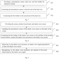
- a method for producing a piezoelectric sensor of an interactive board including:
- a method for producing an elastic wave sensor including:
- a method for producing an interactive board including:
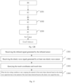
- a material recognizing method is provided, which is applied to an interactive board of any one of embodiment of the present disclosure.
- the method includes:
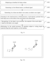
- a writing method which is applied to an interactive board of any one of embodiments of the present disclosure, the method includes:
- an interactive board including an elastic wave sensor and an elastic wave processor of any one of embodiments of the present disclosure
- an interactive board including a screen, a central processing unit, an elastic wave sensor of any one of embodiments of the present disclosure, an elastic wave processor, an infrared sensor, and an infrared processor;
- an interactive board including:
- a computer readable storage medium stores a computer program, the computer program is used to enable a processor to execute the material recognition method of any one of embodiments of the present disclosure or the writing method of any one of embodiments of the present disclosure.
- a computer program product including a computer program, when the computer program is executed by a processor, a material recognition method of any one of embodiments of the present disclosure or a writing method of any one of embodiments of the present disclosure is implemented.
- the piezoelectric sensor includes a piezoelectric structure and an electrode, the electrode covers the surface of a part of the piezoelectric structure; the working frequency of the piezoelectric sensor is matched with the material frequency, the material frequency is the frequency used to distinguish the material of the touch object in the elastic wave generated by the screen of the interactive board when being touched by a touch object such as a hand and a stylus; under this condition, the piezoelectric sensor can enhance a sensitivity of detecting elastic waves generated by a conventional touch object such as the hand and the stylus when writing on the screen of the interactive board.
- the piezoelectric sensor to detect the elastic waves generated when the touch object touches the screen surface, thereby generating high-quality elastic wave signals and improving the accuracy of detecting the material of the touch object such as the hand and the stylus in the scenario of the interactive board, providing a perceptual basis for adding a material recognition function to the interactive board.
- the material recognition function can increase the diversity of writing functions in the interactive board, enhance the functionality of certain writing related operation in the interactive board, simplify the convenience of a certain operation related to writing in the interactive board, and thus improve the service quality of the interactive board.
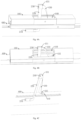
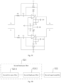
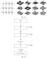
- Figs. 1A-1E , 2A-2K , 3A-3E , 4A-4E , and 5A-5F 100. Interactive board; 101. First frame; 102. Second frame; 103. Third frame; 104. Fourth frame; 105. Frame; 106. Central processing unit; 107. Infrared processor; 108. Elastic wave processor; 110. Screen; 111. Ink; 112. LCD panel; 120. Infrared sensor; 121. Infrared transmitter; 122. Infrared receiver; 131. First touch state; 132. Second touch state; 133. Third touch state; 134. Fourth touch state; 135. Fifth touch state; 200. Elastic wave sensor; 201. First surface; 202. Second surface; 203.
- First high-pass filter 512. First signal amplifier; 520. Secondary preprocessing circuit; 521. Second band-pass filter; 5211. Second low-pass filter; 5212. Second high-pass filter; 522. Second signal amplifier; 523. Common mode voltage filter; 524. First direct current (DC) blocking circuit; 525. First voltage bias circuit; 526. Second DC blocking circuit; 527. Second voltage bias circuit.
- DC direct current
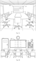
- Fig. 1A in office business scenarios, users use an interactive board 100 to assist meetings in the meeting room, and as shown in Fig. 1B , in teaching business scenarios, users use an interactive board 100 to assist classes in the classroom.
- An interactive board integrates one or more functions such as projector, electronic whiteboard, screen, audio, television and video conference terminal.
- the interactive board may be composed of one physical entity or two or more physical entity.
- these physical entities include a screen 110, and the screen may be used to display various information, and its types may include LED (Light Emitting Diode) screen, OLED (Organic Light Emitting Diode) screen, LCD (Liquid Crystal Display) screen, and the like.
- LED Light Emitting Diode
- OLED Organic Light Emitting Diode
- LCD Liquid Crystal Display
- interactive boards may establish data connections with at least one external device.
- the external devices include but are not limited to: mobile phones, laptops, USB (Universal Serial Bus) flash drives, USB screen drivers (such as USB Dongles), tablets, desktops, and other interactive boards.
- USB Universal Serial Bus
- USB screen drivers such as USB Dongles
- tablets desktops, and other interactive boards.
- Interactive boards may manipulate the information displayed on the screen through the touch technology, thus achieving human-computer interaction. That is, a user interface (UI) is displayed on the screen, and the user touches the screen surface by a touch object. At this time, the positioning operation is performed to locate a position of a touch object on the screen, triggering the corresponding position function on the interface.
- UI user interface
- the hand may include portions such as the fingertips, knuckles, palms, and back of the hand.
- Styluses also known as handwriting pens, are generally components that manufacturers of interactive boards provide for interactive boards.
- a material with high reflectivity for an infrared signal may be added at the stylus head and a position of the stylus body near the stylus head to improve the sensitivity of the stylus in an infrared touch system.
- a controller and one or more sensors may be added inside the stylus.
- the controller is a logical device that controls the stylus, which is electrically connected to the sensor to achieve different functions for the interactive board in conjunction with the sensor.
- the senor may include a Bluetooth module, a Wi-Fi module, a vibration sensor, a pressure sensor, and the like.
- a communicable sensor such as a Bluetooth module and a Wi-Fi module establishes wireless connections with the interactive board to communicate therewith.
- the vibration sensor may generate a vibration simulated tactile sensation when a user is writing, and the pressure sensor may detect a pressure of the writing of the user, which is not limited in this embodiment.
- the interactive board supports multi-touch.
- a single user may use both a hand and a stylus at the same time.
- Multiple fingers and styluses may perform touch operations on the screen surface.
- Multiple users may also use hands or styluses respectively to perform touch operations on the screen surface.
- a protective material on the surface of the display module is the screen surface, which is not limited in this embodiment.
- an application provides wireless screen transfer services, which may perform wireless transfer screen of images from a mobile apparatus such as a computer, a phone, and a tablet to the interactive board.
- a mobile apparatus such as a computer, a phone, and a tablet to the interactive board.
- a timing service and a screen projection service to time duration of a business such as teaching and meeting operations is provided, which avoids timeout and delay, and enables a mobile apparatus on site to scan and vote, thereby improving a decision-making efficiency.
- an application may provide remote multi terminal interaction in meeting and teaching scenarios, the screen is projected and an annotation is added at a terminal in one region, and a terminal in another region display in real time screen projection contents and annotations.
- the infrared beam grid is above the cover plate, and in addition, the infrared beam grid may also be located inside the cover plate or other positions.
- the dense infrared signals in different directions form a beam grid, which uses the changes in the infrared beam grid caused by touch objects to locate touch points.
- multiple infrared emitters are installed on a first side of the frame of the screen, while multiple infrared receivers are installed on a second side of the frame of the screen.
- the first side is opposite to the second side, that is, the infrared receiver is within a scanning range of the infrared transmitter, so that the infrared signal emitted by the infrared emitter is received by the infrared receiver.
- the infrared transmitter and infrared receiver are installed on the same side of the screen frame.
- infrared sensors only include single-ended infrared emitters.
- multiple infrared emitters form a collection and are installed in the form of light strips on the printed circuit board.
- the light strip is designated as first light strip, and the first light strip is provided with an emission driver chip.
- the emission driver chip is connected to multiple infrared emitters and may be configured to provide first control signals to multiple infrared emitters, and control the infrared emitters to emit infrared signals.
- Multiple infrared receivers form a collection and are installed in the form of light strips on the printed circuit board.
- this light strip is designated as second light strip, and the second light strip is provided with a receiving driver chip.
- the receiving driver chip is connected to multiple infrared receivers and may be configured to provide second control signals to multiple infrared receivers, and control the infrared receivers to receive infrared signals.
- the shape of the screen varies, such as rectangles, hexagons, circles, etc.
- the shape of the frame also varies with the shape of the screen, such as rectangles, hexagons, circles, etc.
- the settings of the infrared emitter and receiver in each infrared sensor also vary.
- the shape of the frame of the interactive board is rectangular.
- the frame of the interactive board includes a first frame 101, a second frame 102, a third frame 103, and a fourth frame 104.
- the first frame 101 is opposite to the third frame 103, and in the horizontal direction, the second frame 102 is opposite to the fourth frame 104.
- the first frame 101 is located at the top, hence also known as a sky side
- the third frame 103 is located at the bottom, hence also known as a ground side
- the second frame 102 is also known as a left side
- the fourth frame 104 is also known as a right side.
- the infrared transmitter 121 is arranged on the first frame 101, and the infrared receiver 122 is arranged on the third frame 103.
- the infrared transmitter 121 is arranged on the second frame 102, and the infrared receiver 122 is arranged on the fourth frame 104.
- an infrared processor 107 is installed inside the interactive board.
- the infrared processor 107 is a microcontroller unit (MCU) that is matched with the infrared sensor, such as 811 SOC (System on Chip).
- MCU microcontroller unit
- 811 SOC System on Chip
- the infrared processor may provide touch processing services for upper layer applications or elastic wave processors based on the infrared signals, that is, the infrared processor may process the infrared signal scanned by the infrared sensor on the touch object, such as calculating the coordinates of the touch object (X coordinate, Y coordinate), calculating width and height, marking time of the appearance of the touch object, calculating the cross-sectional area of the touch object, and the like, to form a touch data package (i.e. touch point data).
- a touch data package i.e. touch point data
- the central processing unit has the logical processing ability of infrared signals.
- the CPU may provide touch processing services for upper level applications or elastic wave processors based on the infrared signals. That is, the infrared processor uploads the infrared signals to the CPU, and the CPU may process the infrared signals scanned by the infrared sensor on the touch object. For example, the CPU may calculate the coordinates of the appearance of the touch object (X coordinate, Y coordinate), calculate the width and height, mark the time when the touch object appears, calculate the cross-sectional area of the touch object, and the like, to form a touch data package (i.e. touch point data).
- a touch data package i.e. touch point data
- USB components between the central processing unit 106 and the infrared processing unit 107 such as USB HUB (hub), USB switch, USB Redriver (signal relay), etc.
- the central processing unit 106 may serve as a HID (Human Interface Device), and the infrared processing unit 107 communicates with the central processing unit 106 through USB components.
- HID Human Interface Device
- the infrared processing unit 107 When the infrared processing unit 107 generates touch data packets, the touch data packet is transmitted to the central processor 106, and the touch data packet is reported to the upper layer application of the operating system.
- the screen of the interactive board may also be a capacitive screen, a resistive screen, or an electromagnetic screen, and itself supports touch operation, which is not limited in this embodiment.
- the infrared sensor 120 transmits light through a filter strip (also known as a filter).
- the filter strip is usually made by adding dye to the raw material and using injection molding or casting technology.
- the filter strip may transmit infrared light while filtering out other ambient light, thereby improving a signal-to-noise ratio of the infrared signal.
- the infrared sensor 120 scans the infrared signal on the surface of screen 110 within a certain height range. Therefore, the infrared sensor 120 forms a touch region in the vertical direction of the screen 110, having a height of H, which is generally greater than 2mm (millimeters) and cannot be ignored.
- the general process is to first press the touch object, move the touch object when it touches the screen surface, and finally lift the touch object.
- a partial processing operation of the infrared touch system is described from a first touch state 131, a second touch state 132, a third touch state 133, a fourth touch state 134 to a fifth touch state 135 when the touch object is pressed (Down), moved (Move), and raised (Up) in one touch operation.
- the touch object begins to press and is above the touch region, that is, a distance between the touch object and the plane on which the surface of the screen 120 is located is greater than H, and the infrared signal scanned by the infrared sensor 120 is not blocked by the touch object.
- the infrared processor or central processing unit does not report the touch point data.
- the touch object continues to be pressed and is in the touch region, without touching the surface of the screen 120. That is, the distance between the touch object and the plane on which the surface of the screen 120 is located is greater than 0 and less than H.
- the infrared signal scanned by the infrared sensor 120 is blocked by the touch object.
- the infrared processor or central processor reports the touch point data.
- the touch object is in the touch region and has touched the surface of the screen 120.
- the touch object may be moved on the surface of the screen 120, that is, the distance between the touch object and the plane on which the screen surface is located is less than or equal to 0 (less than 0 indicates a phenomenon that the screen surface is concave under the force of the touch object).
- the distance between the touch object and the surface of the screen 120 is less than H.
- the infrared signal scanned by the infrared sensor 120 is blocked by the touch object, and the infrared processor or central processing unit reports the touch point data.
- the touch object begins to lift and is in the touch region, without touching the surface of the screen 120. That is, the distance between the touch object and the plane on which the surface of the screen 120 is located is greater than 0 and less than H.
- the infrared signal scanned by the infrared sensor 120 is blocked by the touch object.
- the infrared processor or central processor reports the touch point data.
- the touch object continues to lift and be above the touch region, that is, the distance between the touch object and the plane on the surface of the screen 120 is located is greater than H, and the infrared signal scanned by the infrared sensor 120 is not blocked by the touch object.
- the infrared processor or central processing unit does not report touch point data.
- touch apparatuses that users use in their daily lives are mostly mobile phones and tablets. These touch apparatuses often use resistive or capacitive screens, so that most users are accustomed to using resistive or capacitive touch operations. That is, when the touch object touches the screen surface, it will only report touch point data and perform corresponding operations.
- the infrared touch system Due to the habit of using resistive or capacitive touch operations formed by users in long-term life, work, and learning, for interactive boards, the infrared touch system is imperceptible to users. Even if the touch object enters the touch region of the infrared sensor, the touch point data is reported. Considering the high cost of learning infrared touch operations, promotion has certain difficulties, Therefore, regardless of whether the interactive board uses an infrared touch system or a capacitive screen, users currently use resistive or capacitive touch operations on the interactive board, that is, pressing the touch object until it touches the surface screen to achieve touch operations on the interactive board.
- infrared touch operations such as in-glass
- the touch region may be ignored.
- infrared touch operations are basically consistent with resistive touch operations and capacitive touch operations.
- an interactive board using infrared touch technology where the touch object blocks the infrared signal but the actual touch object does not touch the screen surface, will also have the same touch effect as the touch object touching the screen surface. Therefore, it will bring users a bad touch interaction experience.
- the present disclosure creatively introduces an elastic wave sensor. By combining the signals of elastic wave sensors and infrared touch technology, this problem has been solved, providing users with a better touch interaction experience.
- Stress wave is a propagation form of stress and strain disturbance
- the elastic wave is a type of stress wave, that is, the form of stress and strain caused by disturbance or external force transmitted in an elastic medium.
- the frequency of elastic waves generated when a touch object touches the screen surface of an interactive board is determined by the two contact media, that is, the touch object and the screen.
- the two contact media that is, the touch object and the screen.
- low-frequency fundamental waves and higher-order harmonics are generated, and the energy of low-frequency fundamental waves is generally much higher than that of higher-order harmonics.
- a resonant frequency of the piezoelectric sensor is designed to be consistent with the frequency of the fundamental wave, and the frequency of the fundamental wave is positioned as the working frequency for material recognition, so as to improve the signal-to-noise ratio of the piezoelectric sensor (elastic wave sensor) and thus improve the signal-to-noise ratio of the sensor.
- At least one elastic wave sensor is installed on the screen of the interactive board, where a working frequency of the elastic wave sensor is basically matched (also known as being identical) with the frequency (i.e. material frequency) used to distinguish different materials in the elastic wave generated by the touch object touching the screen surface.
- a sensitivity of detecting the elastic wave generated by conventional touch objects such as hands and styluses when writing on the screen in the interactive board can be enhanced, so that the piezoelectric sensor (elastic wave sensor) detects the elastic waves generated when a touch object touches the screen surface, thereby generating high-quality elastic wave signals, improving the accuracy of detecting the material of the touch object such as the hand and the stylus in the scenario of the interactive board, providing a perceptual basis for adding a material recognition function to the interactive board.
- the material recognition function can increase the diversity of writing functions in the interactive board, enhance the functionality of a certain operation related to writing in the interactive board, simplify the convenience of a certain operation related to writing, and thus improve the service quality of the interactive board.
- the elastic wave sensor 200 may include the following structure:
- the piezoelectric sensor is a sensing component that utilizes a piezoelectric effect generated by a certain dielectric material under force, and is a self-generating and electromechanical conversion sensing component.
- the so-called piezoelectric effect refers to a phenomenon where a certain dielectric material undergoes deformation (including bending and stretching deformation) under the action of external forces in a certain direction, resulting in the generation of charges on their surface due to changes in the internal charge distribution of the material.
- the piezoelectric sensor is influenced by an elastic waves and generate elastic wave signals using positive piezoelectric effects.
- the so-called positive piezoelectric effect may refer to that a certain dielectric material in a piezoelectric sensor generates a certain amount of charge on the electrode surface and is in a charged state when a force is applied along a certain direction (such as the deformation caused by the touch object touching the surface of a screen of an interactive board) to make it deform, and returns to a normal uncharged state when the external force is removed.
- a shape of the piezoelectric sensor includes at least one of the followings: a cuboid, a cube, and a cylinder.
- the various structural components in the interactive board are relatively compact, and the original design did not have a piezoelectric sensor, so there was no dedicated space reserved for installing piezoelectric sensors. Therefore, the space available for installing piezoelectric sensors in the original structure of the interactive board is relatively small. For the ease of differentiation, the space available for installing piezoelectric sensors in the interactive board is recorded as the target space. If a cube based piezoelectric sensor and a cylinder based piezoelectric sensor are selected, significant modifications may be required to the original structure of the interactive board. Therefore, in the case of limited target space, in order to reduce changes to the original structure of the interactive board and reduce production costs, this embodiment may select a rectangular piezoelectric sensor.
- the piezoelectric sensor includes the following dimensions:
- a length L of the piezoelectric sensor is designed to be the half wavelength of the elastic wave generated by the touch object on the screen surface. Therefore, at the frequency of the elastic wave, the piezoelectric sensor resonates and generates gain, which enhances the sensitivity of the elastic wave sensor.
- the length L of a piezoelectric sensor refers to the length of an effective working region of the electrodes, and the effective working region refers to certain regions where the electrodes may convert stress into charge.
- electrodes in the certain regions cannot convert stress into charge.
- the regions where these electrodes are located are ineffective working regions, and the ineffective working regions of the electrodes is not calculated within the length L of the piezoelectric sensor.
- the length L of the piezoelectric sensor is designed to be one wavelength of the elastic wave generated by the touch object touching the screen surface, at the frequency of the elastic wave, the electric potential generated by the piezoelectric sensor is mutually offset, so that the sensitivity of the elastic wave sensor decreases.
- touch objects Some commonly used touch objects for users are mainly styluses and hands. For styluses, touch operations may be triggered by their head or by their tail.
- the frequency of the elastic waves generated on the surface of the touch screen is generally 0-5kHz (kHz).
- the frequency of the elastic wave (fundamental frequency) generated when the hands (especially fingers) of the user knock the screen surface of the interactive board is generally within 1kHz, while the frequency of elastic waves generated by friction between the hands (especially fingers) of the user and the screen surface of the interactive board is generally around 15kHz.
- a horizontal axis of a coordinate system is a length of a certain piezoelectric sensor (mm), and a vertical axis of a coordinate system is an elastic wave signal generated by the piezoelectric sensor (V (volts)).
- 2G shows a curve of the elastic wave signal, presented by the elastic wave in a 0-20kHz frequency band detected by this piezoelectric sensor, changing with length (curve corresponding to 1kHz, 2kHz, 3kHz, 4kHz, 5kHz, 6kHz, 7kHz, 8kHz, 9kHz, 10kHz, 11kHz, 12kHz, 13kHz, 14kHz, 15kHz, 16kHz, 17kHz, 18kHz, 19kHz and 20kHz from top to bottom at 10mm (a dashed line on the left in Fig. 2G )).
- the length of the piezoelectric sensor is between 10mm and 30mm (dashed line on the right in Fig. 2G )
- the elastic wave in the 0-20kHz frequency band is enhanced, which may cover some commonly used touch objects. Therefore, in this embodiment, the length of the piezoelectric sensor of the elastic wave sensor is between 10mm and 30mm, including 10mm and 30mm.
- an intermediate value of 20mm may be selected as the length of the piezoelectric sensor.
- the piezoelectric sensor may generate a certain gain for some commonly used touch objects by users, and has wide applicability.
- a length L of 20mm for a piezoelectric sensor allows for certain errors (also known as tolerances).
- the error of the length L for a piezoelectric sensor is expressed as 20mm ⁇ 0.3mm, which means that a maximum of 0.3mm is allowed on the basis of 20mm, a maximum of 0.3mm is allowed on the basis of 20mm, and a range of 19.7mm-20.3mm may be considered as an error range.
- the length of a piezoelectric sensor may be considered as 20mm.
- the error of the length L of the piezoelectric sensor may be used to control the capacitance error of the elastic wave sensor.
- the error of the length L of the piezoelectric sensor should be consistent to ensure the consistency of the capacitance of the elastic wave sensor.
- the width W of a piezoelectric sensor is the same as the length L of the piezoelectric sensor, which will improve the performance of the piezoelectric sensor.
- the width of the piezoelectric sensor is correspondingly 10mm-30mm.
- the width of the piezoelectric sensor is correspondingly preferably 20mm.
- this embodiment may shorten the width W of the piezoelectric sensor, that is, the width W of the piezoelectric sensor is smaller than the length L of the piezoelectric sensor.
- the basic requirement for the width W of piezoelectric sensors is that the width of the piezoelectric sensor is smaller than the width of the target space, so that the piezoelectric sensor may be installed in the target space of the interactive board.
- the width of the target space that may be used to install piezoelectric sensors in interactive boards is about 10mm, so the width W of piezoelectric sensors may be designed to be less than 10mm.
- the width W of the piezoelectric sensor may be designed to be 5mm, making it easy to install the piezoelectric sensor on the screen of the interactive board using the corresponding process.
- a width W of 5mm for a piezoelectric sensor allows for certain errors.
- the error of the width W of a piezoelectric sensor is expressed as 5mm ⁇ 0.1mm, which means that a maximum of 0.1mm is allowed on the basis of 5mm and a maximum of 0.1mm is allowed on the basis of 5mm.
- the width of a piezoelectric sensor may be considered as 5mm.
- the error of the width W of the piezoelectric sensor may be used to control the capacitance error of the elastic wave sensor.
- the error of the width W of the piezoelectric sensor should be consistent to ensure the consistency of the capacitance of the elastic wave sensor.
- the thickness T of a sensor is also known as height, considering that the capacitance value of a piezoelectric sensor is inversely proportional to the thickness T of the sensor. That is, the thicker the piezoelectric sensor, the smaller its capacitance value. Therefore, in an ideal situation, the larger the thickness T of a piezoelectric sensor, the better the performance of an elastic wave sensor.
- the basic requirement for the thickness T of piezoelectric sensors is that the thickness T of the piezoelectric sensor is less than the height of the target space, so that the piezoelectric sensor may be installed in the target space of the interactive board.
- operational amplifiers are used to amplify the small charges generated by piezoelectric sensors. From the positive piezoelectric effect of piezoelectric sensors, it may be seen that when the piezoelectric sensor undergoes deformation under force, a certain amount of charge is generated.
- parasitic capacitance C e may be ignored. If the capacitance C p of the piezoelectric sensor itself is less than parasitic capacitance C e .
- the output voltage is influenced by the parasitic capacitance C e , which makes the circuit unstable, therefore, the capacitance C p of the piezoelectric sensor itself cannot be as small as possible.
- the height of the target space that may be used to install piezoelectric sensors in an interactive board is about 10mm, so the thickness T of the elastic wave sensor may be designed to be less than 10mm.
- the thickness T of the piezoelectric sensor may be designed to be 2mm.
- the thickness T of a piezoelectric sensor is 2mm, which allows for certain errors.
- the error of the thickness T of a piezoelectric sensor is expressed as 2mm ⁇ 0.08mm, which means that a maximum of 0.08mm is allowed on the basis of 2mm, a maximum of 0.08mm is allowed on the basis of 2mm, and a range of 1.92mm to 2.08mm may be considered as an error range. Within this error range, the thickness of a piezoelectric sensor may be considered as 2mm.
- the error of the thickness T of the piezoelectric sensor may be used to control the capacitance error of the elastic wave sensor.
- the error of the thickness T of the piezoelectric sensor should be consistent to ensure the consistency of the capacitance of the elastic wave sensor.
- the piezoelectric sensor exhibits a piezoelectric effect after polarization, and its polarization direction is in the direction of the thickness T.
- the piezoelectric sensor has the following structure:
- the piezoelectric sensor has at least one layer of a piezoelectric structure 211.
- the piezoelectric structure 211 is a component made of a piezoelectric material (i.e. a sensitive functional material that exhibits a piezoelectric effect).
- the materials of piezoelectric structures may include piezoelectric crystals, piezoelectric ceramics, organic piezoelectric materials, piezoelectric polymer materials, such as PZT (Pb (Zr 1-x TiO 3 ), lead zirconate titanate), BaTiO 3 (barium titanate), AlN (aluminum nitride), ZnO (zinc oxide), PVDF (polyvinylidene fluoride), and the like.
- PZT Pb (Zr 1-x TiO 3
- lead zirconate titanate lead zirconate titanate
- BaTiO 3 barium titanate
- AlN aluminum nitride
- ZnO zinc oxide
- PVDF polyvinylidene fluoride
- the material of the piezoelectric structure may be selected as PZT.
- PZT may be classified into different categories, such as PZT-2 (lead zirconate titanate 2 series), PZT-4 (lead zirconate titanate 4 series), PZT-5 (lead zirconate titanate 5 series), and PZT-8 (lead zirconate titanate 8 series).
- PZT-5 is a soft material.
- the material of the piezoelectric structure may be selected as PZT-5, which includes PZT-5A, PZT-5D, PZT-5J, PZT-5H, PZT-5X, and the like.
- the components of these materials are different, and the specific performance shows differences, that is, the dielectric constant, dielectric loss, electromechanical coupling coefficient, and piezoelectric constant may all vary.
- optional materials may be selected based on the business requirements of material recognition.
- the adhesion force of the electrode is greater than 2.5N/mm 2 (N/square millimeter), which may meet the stability of elastic filter performance.
- the material of the electrode may be preferably silver, that is, the surface of the piezoelectric structure is covered with a silver layer, and the electrode formed by silver may meet the requirements of resistance, adhesion, etc.
- the electrode material may also be copper, aluminum, gold, and other materials, which is not limited in this embodiment.
- the electrodes may be divided into a first electrode 212 and a second electrode 213.
- the first electrode 212 and the second electrode 213 are independent and not connected to each other, and may serve as positive and negative electrodes, respectively.
- a flanging design may be used for the first electrode 212 and the second electrode 213.
- the flanging design is not only convenient for installing piezoelectric sensors, but also for connecting lead wires to the first electrode 212 and the second electrode 213.
- the piezoelectric structure (piezoelectric sensor) includes a first surface 201, a second surface 202, and a third surface 203 adjacent to both the first surface 201 and the second surface 202.
- the first surface 201 and the second surface 202 are generally the two surfaces with the largest area and independent of each other in the piezoelectric structure (piezoelectric sensor).
- the area of the first surface 201 is usually equal to that of the second surface 202.
- the first surface 201 is the upper surface in the piezoelectric structure (piezoelectric sensor)
- the second surface 202 is the lower surface in the piezoelectric structure (piezoelectric sensor).
- the third surface 203 is a surface that is adjacent to both the first surface 201 and the second surface 202 along the length L direction, such as the side surface in a piezoelectric structure (piezoelectric sensor). Adjacency may refer to the first surface 201 having a common side with the third surface 203, and the second surface 202 having a common side with the third surface 203.
- piezoelectric structures have a large number of side surfaces, such as rectangular, cubic, and other shaped piezoelectric structures (piezoelectric sensors), which have four side surfaces, and the third surface 203 is one of the independent side surfaces.
- the second electrode 213 may cover the whole third surface 203.
- the first electrode 212 covers a part of the first surface 201
- the second electrode 213 covers a part of the first surface 201, the whole second surface 202, and a part of the third surface 203 or the whole third surface 203, respectively. That is, the second electrode 213 is led from the second surface 202 to the first surface 201 through the third surface 203, thereby forming an easily connected positive and negative electrodes with the first electrode 212 of the first surface 201.
- the first electrode 212 covers the first side of the first surface 201
- the second electrode 213 covers the second side of the first surface 201
- the first side is opposite to the second side. If the first side is on the left, the second side is on the right, and if the first side is on the right, the second side is on the left.
- the area of the first electrode 212 is greater than that of the first gap, and the area of the first gap is greater than that of the second electrode 213, then the area of the first electrode 212 is greater than that of the second electrode 213.
- the first surface 201 is the upper surface of the piezoelectric structure (piezoelectric sensor)
- the first surface 201 is a rectangle
- the second surface 202 is the lower surface of the piezoelectric structure (piezoelectric sensor)
- the second surface 202 is a rectangle.
- the shape of the first gap is also rectangular.
- a width W of the first electrode 212 is the same as that of the piezoelectric sensor (piezoelectric structure), a width W of the second electrode 213 is the same as that of the piezoelectric sensor (piezoelectric structure), and the width W of the first gap is the same as that of the piezoelectric sensor (piezoelectric structure), that is, the width W of the first electrode 212, the width W of the second electrode 213, and the width of the first gap are equal.
- the length L1 of the first electrode 212 is greater than that of the first gap, and the length L2 of the first gap is greater than that of the second electrode 213.
- the length L1 of the first electrode 212 is greater than the length L3 of the first gap, and the length L3 of the first gap is greater than the length L2 of the second electrode 213.
- the length L1 of the first electrode 212 is greater than the length L2 of the second electrode 213.
- the length L3 of the first gap is greater than the thickness T of the piezoelectric sensor.
- the second electrode 213 located on the second surface 202 is in the effective working region, and the second electrode 213 located on the first surface 201 and the second electrode 213 located on the third surface 203 are both in the ineffective working region. Therefore, the length L of the piezoelectric sensor refers to the length of the second electrode 213 located on the second surface 202, and does not incorporate the second electrode 213 located on the first surface 201, the second electrode 213 located on the third surface 203 into the length L of the piezoelectric sensor.
- the length L1 of the first electrode 212 is 17mm
- the width W is 5mm
- the length L2 of the second electrode 213 is 1mm
- the width W is 5mm
- the length L3 of the first gap is 2mm
- the width W is 5mm.
- the length of the second electrode 213 is denoted as the length L of the piezoelectric sensor, which is 20mm.
- the length of the second electrode 213 is denoted as the thickness T of the piezoelectric sensor, which is 2mm.
- the length L1 of the first electrode 212 is 17mm
- the length L2 of the second electrode 213 is 1mm
- the length L3 of the first gap is 2mm, which allows for certain errors.
- the error of the length L1 of the first electrode 212 is expressed as 17mm ⁇ 0.2mm, that is, the minimum of 0.2mm is allowed on the basis of 17mm, the maximum of 0.2mm is allowed on the basis of 17mm, and the range of 16.8mm to 17.2mm may be considered as the range of errors.
- the length L1 of the first electrode 212 is 17mm; the error of the length L2 of the second electrode 213 is expressed as 1mm ⁇ 0.1mm, which means that a maximum of 0.1mm is allowed on the basis of 1mm, and a maximum of 0.1mm is allowed on the basis of 1mm, and a range of 0.9mm-1.1mm may be considered as an error range.
- the length L2 of the second electrode 213 may be considered as 1mm; the error of the length L3 of the first gap being 2mm is expressed as 2mm ⁇ 0.1mm, which means that a maximum of 0.1mm is allowed on the basis of 2mm, and a maximum of 0.1mm is allowed on the basis of 2mm, and a range of 1.9mm-2.1mm may be considered as an error range.
- the length L3 of the first gap may be considered as 2mm.
- the above-mentioned piezoelectric sensor is used to detect the elastic waves generated by two different materials of touch objects when the screen surface is touched.
- the elastic wave signal shown in Fig. 2H is obtained in the frequency domain
- the elastic wave signal shown in Fig. 2I is obtained in the time domain. Whether it is the frequency domain or time domain, the elastic wave signals corresponding to different materials of touch objects are clearly distinguished. It is beneficial to improve the accuracy of using elastic wave signals in the frequency domain and/or time domain to recognize the material of the touch object.
- piezoelectric structures may have other surfaces besides the first surface 201, the second surface 202, and the third surface 203, which do not cover the electrodes.
- the electrode of the piezoelectric sensor is pasted on the screen of the interactive board, so the polarization direction of the piezoelectric sensor is perpendicular to the plane on which the screen of the interactive board is located.
- the elastic waves diffuse to various positions in the screen of the interactive board, and may even be transmitted to other parts in direct or indirect contact with the screen in the interactive board.
- the position of the elastic wave transmission includes the position of the piezoelectric sensor.
- the position where the piezoelectric sensor is installed also undergoes bending deformation.
- the stress generated by bending deformation acts on the surface of the piezoelectric sensor, causing deformation of the piezoelectric sensor, so that charges are generated.
- the piezoelectric sensor 210 itself is also a capacitor.
- the charge fills the piezoelectric capacitor, a voltage is generated at both ends of the piezoelectric sensor 210 to convert mechanical energy into electrical energy.
- the first end of the lead wire is connected to the piezoelectric sensor 210, especially the electrode of the piezoelectric sensor 210.
- the second end of the lead wire is connected to the first holder 230, especially the pin in the first holder 230.
- the lead wire is used for transmitting elastic wave signals generated by the piezoelectric sensor 210.
- the lead wire is generally a flexible wire, that is, a wire with bending characteristics, which has a high fault tolerance for the installation position of piezoelectric sensor 210 and the wiring of the first holder 230, which can improve the convenience of installing and connecting elastic wave sensor 200 in an interactive board, and improve production efficiency.
- the form of transmitting elastic wave signals is differential transmission, that is, the elastic wave signal is a differential signal, which is also known as a differential mode signal, and is relative to a common mode signal.
- the differential signal transmits signals on both lines, with equal amplitudes and opposite phases, thus using a numerical value to represent the difference between two physical quantities.
- the lead wire for transmitting elastic wave signals there are two lines in the lead wire for transmitting elastic wave signals, of which one is connected to the positive electrode (such as the first electrode 212) in the electrode of the piezoelectric sensor 210, and the other is connected to the negative electrode (such as the second electrode 213 located on the first surface 201) in the electrode of the piezoelectric sensor 210.
- the above forms of transmitting elastic wave signals and the number of lines are only examples.
- other forms of transmitting elastic wave signals and the number of lines may be set according to the actual situation.
- the form of transmitting elastic wave signals is single ended transmission, that is, the elastic wave signal is a single ended signal.
- a grounded line is connected to the electrode of the piezoelectric sensor, and the difference between the piezoelectric sensor and the ground is detected as an elastic wave signal, etc., which is not limited in this embodiment.
- those skilled in the art may also use other forms of transmitting elastic wave signals and number of lines according to actual requirements, which is not limited in this embodiment.
- This embodiment may select the corresponding form of lead wire based on comprehensive considerations in production, performance, and other aspects, and then select the process of connecting the lead wire to the piezoelectric sensor 210 (especially the electrode of the piezoelectric sensor 210).
- the lead wire connected to the piezoelectric sensor 210 is a flexible printed circuit (FPC), and for ease of differentiation, the flexible printed circuit is denoted as the first flexible circuit board 220.
- FPC flexible printed circuit
- the flexible circuit board also known as soft circuit board and flexible printed circuit board, is a kind of highly reliable and flexible printed circuit board made of polyimide or polyester film and other materials. It has the characteristics of high wiring density, light weight, thin thickness and good flexibility, which is convenient to install in the interactive board.
- the number of solder pads in the first flexible circuit board 220 is equal to that of electrodes in the piezoelectric sensor 210.
- a size of the first solder pad 221 matches with the size of the first electrode 212. Matching may refer to the size of the first solder pad 221 being less than or equal to that of the first electrode 212. If the first electrode 212 is rectangular and the first solder pad 221 is also rectangular, the length of the first solder pad 221 is less than or equal to the length of the first electrode 212, and/or the width of the first solder pad 221 is less than or equal to that of the first electrode 212, so that the first solder pad 221 is connected to the first electrode 212.
- the first solder pad 221 on the first flexible circuit board 220 has a length of 2mm and a width of 3.8mm
- the second solder pad 222 has a length of 1mm and a width of 3.8mm
- the second gap between the first solder pad 221 and the second solder pad 222 has a length of 2mm and a width of 3.8mm.
- a first adhesive 223 may be added between the third surface 203 and the first flexible circuit board 220.
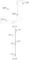
- the first flexible circuit board 220 may be designed as a connected first plate 224 and second plate 225, where the first plate 224 is perpendicular to the second plate 225, and the length of the first plate 224 is smaller than that of the second plate 225, that is, the first flexible circuit board as a whole presents an "L" shape.
- the first end of the line in the first flexible circuit board 220 is located on the first plate 224, that is, the piezoelectric sensor 210 is connected to the first plate 224.
- the second end of the line in the first flexible circuit board 220 is located on the second plate 225, that is, the first holder 230 is connected to the second plate 225.
- the lead wires are two single-stranded connecting wires 240. At this time, different colors may be configured for each single-strand connecting wire 240 to distinguish the wiring.
- one single-strand connection wire 240 is welded to the first electrode 212 of the piezoelectric sensor 210, and the other single-strand connection wire 240 is welded to the second electrode 213 of the piezoelectric sensor 210.
- the second end of the line on the lead wire (such as the first flexible circuit board 220) is connected to a holder, and for ease of differentiation, the holder is denoted as the first holder 230.
- multiple pins pin may be designed based on the characteristics of the elastic wave signal, and the number of pins pin is related to the form of transmitting elastic wave signals.
- the first holder 230 in the case of transmitting elastic wave signals in differential form, includes at least two pins, which are respectively used to transmit two signals (positive signal and negative signal) with equal amplitude and opposite phases in the elastic wave signal.
- first holder 230 includes two pins to ensure wiring stability, two pins may be used.
- the first holder 230 includes at least four pins, of which two are used for transmitting elastic wave signals in differential form, and the other at least two pins are grounded.
- the two pins used for transmitting elastic wave signals are arranged in the middle of all pins, that is, the two pins used for transmitting elastic wave signals are arranged by the grounded pins, which may not only shield the signal from the ground to ensure the quality of the elastic wave signal, but also increase the volume of the first holder 230 to facilitate carrying the buckle, thereby preventing the wiring from loosening and ensuring the stability of the wiring.
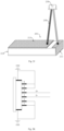
- the first holder includes six pins, which are arranged in sequence from bottom to top, denoted as the first pin (1), the second pin (2), the third pin (3), the fourth pin (4), the fifth pin (5), and the sixth pin (6).
- the first pin (1), second pin (2), fifth pin (5), and sixth pin (6) are all grounded to GND
- the third pin (3) and fourth pin (4) are used to transmit the elastic wave signal generated by the piezoelectric structure in differential form
- the third pin (3) is used to transmit the positive signal D+ in the elastic wave signal
- the fourth pin (4) is used to transmit the negative signal D- in the elastic wave signal.
- the first pin (1) and the second pin (2) are located on the first side of the third pin (3) and the fourth pin (4), the fifth pin (5) and the sixth pin (6) are located on the second side of the third pin (3) and the fourth pin (4), that is, the first pin (1) and the second pin (2) are located on one edge of the first holder 230, and the fifth pin (5) and sixth pin (6) are located on the other edge of the first holder 230, the third pin (3) and the fourth pin (4) are located in the middle of the first holder 230.
- the elastic wave sensor has high sensitivity in detecting the elastic wave generated by the touch object touching the screen surface of the interactive board, which ensures the quality of the elastic wave signal, provides basic conditions for recognizing the material of the touch object and other services, thereby improving the diversity of touch operations, and enriching the functions of the interactive board.
- elastic wave sensors may be installed at any position on the screen capable of transmitting the generated elastic waves, which may be any position on the screen or any position that has direct or indirect contact with the screen, and may detect the elastic waves generated by the touch object touching the screen surface.
- the elastic wave sensor 200 may be installed on the back of the screen 110 to directly receive elastic waves transmitted from the surface of the screen 110, thereby improving detection accuracy.
- the back of the screen 110 is a surface facing the interior of the interactive board, which is not visible to the user.
- the screen 110 is mostly a cover plate, which means that elastic wave sensor 200 may be installed on the back of the cover plate.
- an elastic wave sensor when installed in a center of the back of the screen, its detection accuracy is better.
- the elastic wave sensor may affect the visible region of the screen, thereby affecting the display effect of the screen.
- the elastic wave sensor 200 may be installed at the edge of the back of the screen 110 and outside the visible region of the screen.
- the edge of the back of the screen 110 and a part of region or the whole region outside the visible region of the screen 110 are covered with the ink 111, which may provide insulation, acid resistance, moisture resistance, and protection. Therefore, the elastic wave sensor 200 may be installed at the edge of the back of the screen 110 and the region outside the visible region of the screen 110 covered with the ink 111.
- the structure of the elastic wave sensor 200 includes a piezoelectric sensor 210, a lead wire (such as the first flexible circuit board 220), and a first holder 230.
- the piezoelectric sensor 210 is mainly used to detect elastic waves and generate elastic wave signals, while the lead wire (such as the first flexible circuit board 220) and the first holder 230 are mainly used to transmit elastic wave signals. Therefore, when elastic wave sensor 200 is installed, at least the piezoelectric sensor 210 may be tightly attached to the back of the screen, while the lead wire (such as the first flexible circuit board 220) and the first holder 230 do not require to be tightly attached to the back of the screen.
- the first surface 201 of the piezoelectric sensor 210 is connected to a lead wire (such as the first flexible circuit board 220), and thus, the second surface 202 of the piezoelectric sensor 210 is tightly attached to the back of the screen.
- this embodiment may add a second adhesive 300 between the piezoelectric sensor 210 (especially the second surface 202 of the piezoelectric sensor 210) and the back of the screen 110, so that a second adhesive 300 is presented between the piezoelectric sensor 210 (especially the second surface 202 of the piezoelectric sensor 210) and the back of the screen 110, so as to attach the piezoelectric sensor 210 to the back of the screen 110 of the interactive board.
- the second adhesive 300 forms an adhesive layer between the piezoelectric sensor 210 (especially the second surface 202 of the piezoelectric sensor 210) and the back of the screen 110 of the interactive board.
- an appropriate amount of the second adhesive may be firstly applied to the piezoelectric sensor 210 (especially the second surface 202 of the piezoelectric sensor 210), and then the side of the piezoelectric sensor 210 coated with a second adhesive is placed at a fixed position on the back of the screen 110, and finally a fixture is used to maintain the pressure of the piezoelectric sensor 210.
- the pressure maintaining operation may ensure that the adhesion is tight and the thickness of the adhesive layer meets the requirements.
- the adhesion process also needs to ensure that there is less adhesive overflow, and there are no bubbles in the second adhesive water.
- this embodiment requires at least one of the followings requirements for the second adhesive design to meet the sensitivity requirements.
- This embodiment requires a high Young's modulus of the second adhesive to ensure that the piezoelectric sensor is tightly attached to the back of the screen, ensuring the efficiency of elastic wave transmission from the screen surface to the piezoelectric sensor.
- the Young's modulus is a measure of the stiffness of a solid under load or its resistance to elastic deformation.
- the second adhesive appears to be too soft and unable to effectively transmit deformation.
- the deformation variable transmitted to the piezoelectric sensor of the elastic wave sensor significantly decreases, resulting in a decrease in the amplitude (i.e. distortion) of the electrical signal (i.e. elastic wave signal) output by the piezoelectric sensor of the elastic wave sensor, and even the elastic wave cannot be transmitted to the piezoelectric sensor of the elastic wave sensor.
- piezoelectric sensors with different Young's moduli may be attached to the back of the screen by using previously adhesive, and the attachment effect may be tested. Based on the experimental results, a threshold is designed for the Young's modulus. When the Young's modulus of the second adhesive is greater than this threshold, it may be considered that the second adhesive may tightly attach the piezoelectric sensor to the back of the screen. For easy identification, this threshold is denoted as the installation threshold.
- a mounting threshold is 1GPa (Gigopascals).
- the number of elastic wave sensors is positively correlated with the surface area of the screen of the interactive board. That is, the larger the surface area of the screen of the interactive board, the more elastic wave sensors there are. Conversely, the smaller the surface area of the screen of the interactive board, the fewer the number of elastic wave sensors. At least one elastic wave sensor is installed on the back of the screen of the interactive board, that is, the number of elastic wave sensors should be at least one.
- the number of elastic wave sensors 200 is five, and the elastic wave sensors 200 are located respectively:
- the top left side of the back of the screen 110, the top right side of the back of the screen 110, the bottom left side of the back of the screen 110, the bottom middle of the back of the screen 110, and the bottom right side of the back of the screen 110 all belong to a relative region, which may be set according to the actual situation of the screen 110 and elastic wave sensor 200, which is not limited in this embodiment.
- coordinates with a distance less than the preset first distance threshold from the top side (top edge) of the screen 110 may be divided into the top of the back of the screen 110, or the region of the ink 111 near the top side of the screen 110 may be directly denoted as the top of the back of the screen 110, and the top of the back of the screen 110 may be evenly divided into two regions to distinguish the top left side of the back of the screen 110 and the top right side of the back of the screen 110.
- the elastic wave sensors 200 are installed near the center of the top left side of the back of the screen 110 and near the center of the top right side of the back of the screen 110.
- Coordinates with a distance less than the preset second distance threshold between the bottom side (bottom edge) of the back of the screen 110 may be divided into the bottom of the back of the screen 110, or the region of the ink 111 near the bottom side of the back of the screen 110 may be directly denoted as the bottom of the back of the screen 110, and the bottom of the back of the screen 110 may be evenly divided into three regions to distinguish the bottom left side of the back of the screen 110 and the bottom middle of the back of the screen 110, and the bottom right side of the back of screen 110.
- the elastic wave sensors 200 are installed near the center of the bottom left side of the back of the screen 110, near the center of the bottom middle of the back of the screen 110, and near the center of the bottom right side of the back of the screen 110.
- the number of the elastic wave sensors are four, which are respectively installed on the top left side of the back of the screen, on the top right side of the back of the screen, on the bottom left side of the back of the screen, on the bottom right side of the back of the screen, and the like, which is not limited in this embodiment.
- those skilled in the art may also set the number and their installation positions of other elastic wave sensors according to actual requirements, which is not limited in this embodiment.
- an elastic wave processor 108 is installed in the interactive board.
- the elastic wave processor 108 is a MCU matched with an elastic wave sensor, and the elastic wave processor may provide at least material recognition services for the touch object based on the elastic wave signal, that is, recognition of the material of the touch object based on the elastic wave signal.
- USB components between the central processing unit 106 and the elastic wave processor 108 such as USB HUB (hub), USB switch, USB Rediver (signal relay), etc.
- the central processing unit 106 may serve as an HID, and the elastic wave processor 108 communicates with the central processing unit 106 through USB components.
- the elastic wave processor 108 When the elastic wave processor 108 generates information about the material of the touch object, the material and other information of the touch object are transmitted to the central processing unit 106, so as to report the material and other information of the touch object to the upper application of the operating system.
- the infrared signal and elastic wave signal are specific to the characteristics of the same touch object in different dimensions. Therefore, there is a certain correlation between the infrared signal and elastic wave signal, which may be mutually referenced and corrected.
- the central processing unit 106 may perform logical processing on touch point data or infrared signals provided by the infrared processor 107, information that may assist in processing elastic wave signals is generated, and this information is fed back to the elastic wave processor 108 to assist the elastic wave processor 108 in processing elastic wave information, thereby improving the computing ability and service quality of the elastic wave processor 108.
- both the elastic wave processor 108 and the infrared processor 107 are independent electronic components, which reduces the coupling between various functional systems of the interactive board, avoids the problem of thread preemption, and ensures the normal operation of the interactive panel as much as possible.
- the infrared processor 107 is provided with logic code for processing infrared signals
- the elastic wave processor 108 is provided with logic code for processing elastic wave signals. Assuming that the elastic wave processor 108 and the infrared processor 107 are merged into the same electronic component, that is, the elastic wave processor 108 and the infrared processor 107 are different logical functional units in the same electronic component.
- One of the development efforts to merge the elastic wave processor 108 with the infrared processor 107 is to merge the logic code for processing infrared signals with the logic code for processing elastic wave signals.
- the logic code for processing infrared signals has become relatively mature and stable, while the logic code for processing elastic wave signals is a newly developed logic code that lacks practical verification and may have unknown vulnerabilities Bug, which has already brought unknown risks to the operation of the interaction board.
- the elastic wave processor 108 and the infrared processor 107 are independent of each other, that is, the logical code for processing elastic wave signals in the elastic wave processor 108 is independent of the logical code for processing infrared signals in the infrared processor 107, which may avoid making changes to the logical code for processing infrared signals, avoid introducing vulnerabilities Bug caused by changing the logical code for infrared signals, ensure the stability of the interactive board, reduce development workload, and reduce development costs.
- the elastic wave processor 108 and the infrared processor 107 may be combined into the same electronic component under the condition of ensuring the stable operation of the interactive board, that is, the elastic wave processor 108 and the infrared processor 107 are different logical function units in the same electronic component (such as MCU), and the communication and scheduling between the logical function units are convenient, thereby facilitating the synchronization of functions of the interactive board and improving the performance of interactive boards, which is limited in this embodiment.
- this embodiment proposes the following new layout manner applied to elastic wave sensors on interactive boards.
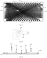
- At least one independent printed circuit board 400 may be arranged in each frame 105 (i.e. the first frame 101, second frame 102, third frame 103, and fourth frame 104 in Fig. 1C ). If there are at least two independent printed circuit boards in the same frame 105, the adjacent printed circuit boards 400 in the same frame 105 are connected through a second flexible circuit board 400.
- the two printed circuit boards 400 are located in the adjacent frame 105 (the left side of the first frame 101 is adjacent to the second frame 102, the right side of the first frame 101 is adjacent to the fourth frame 104, the left side of the third frame 103 is adjacent to the second frame 102, and the right side of the third frame 103 is adjacent to the fourth frame 104), the two printed circuit boards 400 are connected through a second flexible circuit board 400.
- a transmission link may be constructed between the elastic wave processor 108 and the elastic wave sensor 200, which is usually the shortest path transmission link, so as to reduce interference with the elastic wave signal and ensure the quality of the elastic wave signal.
- the direction of connection is along the transmission direction of the elastic wave signal, that is, along the transmission direction of the elastic wave signal, the previous printed circuit board 400 is connected to the next printed circuit board 400 through a second flexible circuit board 400.
- two transmission links may be constructed for this.
- the first transmission link and its transmission direction are:
- the second transmission link and its transmission direction are:
- the printed circuit board 400 located on the rightmost side of the first frame 101 is connected to the printed circuit board 400 located on the top of the fourth frame 104 through a second flexible circuit board 400, and the printed circuit board 400 located on the bottom of the fourth frame 104 is connected to the printed circuit board 400 located on the rightmost side of the third frame 103 through the second flexible circuit board 400.
- the printed circuit board 400 located at the bottom of the second frame 102 and the printed circuit board 400 located at the leftmost side of the third frame 103 are connected through the second flexible circuit board 400.
- the printed circuit board 400 located on the leftmost side of the first frame 101 is not connected to the printed circuit board 400 located on the top of the second frame 102 through the second flexible circuit board 400.
- the first and second transmission links may coexist in the interactive board, thus covering the interactive board.
- both the first and second transmission links may be fully used or partially used, which is not limited in this embodiment.
- transmission links are only examples. When this embodiment is implemented, other transmission links may be arranged based on the actual number and distribution of elastic wave sensors, which is not limited in this embodiment. Moreover, in addition to the above-mentioned transmission links, those skilled in the art may also use other transmission links according to actual requirements, which is not limited in this embodiment.
- these printed circuit boards are arranged with infrared emitters and infrared receivers, provided with at least one lines for transmitting infrared signals, and a circuit for preprocessing infrared signals.
- this circuit is denoted as an infrared line.
- At least one line for transmitting elastic wave signals may be added to the printed circuit board on the basis of the original design.
- this line is denoted as an elastic wave line, which is ultimately connected to the elastic wave processor.
- the elastic wave line is located on the printed circuit board, which may greatly protect the elastic wave signal and greatly reduce interference as compared with external wiring. Not only does it have high stability, but it may also reduce the use of external wires and reduce costs.
- the fixed wiring of elastic wave lines on printed circuit boards may ensure consistency.
- an elastic wave line on a certain printed circuit board 400 provides an interface 410 to the outside.
- the elastic wave sensor 200 is connected to the elastic wave line on the printed circuit board 400, so that after generating the elastic wave signal, the elastic wave sensor 200 may be transmitted it to the elastic wave processor through the elastic wave line.
- the infrared line and the elastic wave line are independent of each other.
- the infrared line and the elastic wave line do not overlap in parallel, and the infrared line and the elastic wave line are isolated by a ground wire, thereby reducing the interference of the infrared signal on the elastic wave signal and reducing the noise of the elastic wave signal.
- an elastic wave circuit is added to the printed circuit board of the frame, allowing the wiring of the elastic wave sensor to be carried out within the frame, improving the manufacturability of the interactive board machine and thereby improving the production efficiency of the interactive board.
- the elastic wave processor 108 and the infrared processor 107 may be installed on different printed circuit boards 400 or on the same printed circuit board 400, which is not limited in this embodiment.
- the elastic wave processor 108 and the infrared processor 107 may be installed on the printed circuit board 400 belonging to the motherboard.
- this motherboard is typically a printed circuit board 400 located on the rightmost side of the ground side (i.e. the third frame 103) in an interactive board.
- the elastic wave processor 108 and the infrared processor 107 may be connected through serial ports, I2C (Inter Integrated Circuit Bus), SPI (Serial Peripheral Interface), etc. Therefore, the elastic wave processor 108 and the infrared processor 107 may communicate through GPIO (General Purpose Input/Output Port) and other manners, the elastic wave processor 108 and infrared processor 107 may achieve high accuracy and processing efficiency through certain coordination and collaboration.
- I2C Inter Integrated Circuit Bus
- SPI Serial Peripheral Interface
- this embodiment adds an intermediate opening 440 and a corresponding cover body 441 in the profile of the frame 105.
- the cover body 441 may be detachably closed on the surface of the opening 440.
- the cover body 441 may be manually inserted into the surface layer of the opening 440 and the cover body 441 may be manually removed.
- a buckle is arranged between the cover body 441 and the surface layer of the opening 440, and the buckle may lock the cover body 441.
- the surface layer of the opening 440 is provided with holes, which may be aligned with screws to install the cover body 441, and the like.
- the number of interfaces 410 and openings 440 on printed circuit board 400 is the same as that of elastic wave sensors 200.
- the interfaces 410 and openings 440 on printed circuit board 400 correspond one-to-one with elastic wave sensors 200.
- the elastic wave sensor 200 may be connected to the interface 410 on the printed circuit board 400 through the opening 440.
- the number of interfaces 410 on printed circuit board 400 is five, located:
- the number of openings 440 is five, located: on the left side of the sky side (first frame), on the right side of the sky side (first frame), on the left side of the ground side (third frame), in the middle of the ground side (third frame), and on the right side of the ground side (third frame).
- the number of elastic wave sensors 200 is five, located: on the top left side of the back of the screen, on the top right side of the back of the screen, on the bottom left side of the back of the screen, in the bottom middle of the back of the screen, on the bottom right side of the back of the screen.
- the posture of the installation of elastic wave sensor 200 will be adjusted, that is, the length direction of the piezoelectric sensor 200 is the same as that of the screen.
- the lead wires in elastic wave sensor 200 are easy to fold and bend, and under the condition where the position of the opening is given, the position requirements for installing elastic wave sensors (piezoelectric sensors) are not high.
- the first flexible circuit board is L-shaped, the shorter first plate is used to connect to the piezoelectric sensor, and the longer second plate extends into the opening 440 and connects to the interface 410 on the printed circuit board 400 inside the frame 105. Therefore, the projection of opening 440 in the horizontal direction and the projection of elastic wave sensor 200 in the horizontal direction may partially or completely overlap, or there may be some misalignment, and the two do not overlap, which is not limited in this embodiment.
- the width of the profile of the frame 105 there are limitations on the width of the profile of the frame 105.
- the width of the profile of the frame 105 of a certain interactive board is 25.25mm.
- the profile of the frame 105 does not increase the opening 440 on the entire surface.
- a local opening 440 is added in the middle of the profile of the frame 105.
- the size of the opening 440 is limited.
- an opening 440 having a rectangular shape and a size of 40mm ⁇ 14.6mm may be added.
- this embodiment adds a flexible circuit board to the interface 410 of the printed circuit board 400 for the elastic wave sensor 200.
- the flexible circuit board is denoted as the third flexible circuit board 430.
- the first end of the third flexible circuit board 430 is connected to an interface on the printed circuit board 400 to access an elastic wave line.
- the connection manner between the third flexible circuit board 430 and the interface 410 on the printed circuit board is to use a holder, that is, the first end of the third flexible circuit board 430 is provided with a third holder 432, the interface 410 on the printed circuit board 400 is provided with a fourth holder 411, the fourth holder 411 is connected to the elastic wave line, and the third holder 432 is matched with the fourth holder 411.
- the third holder 432 is a male port
- the fourth holder 411 is a female port.
- the third holder may also be a female port
- the fourth holder is a male port, which is not limited in this embodiment.
- the third holder 432 of the third flexible circuit board 430 has been pre-connected to the fourth holder 411 on the printed circuit board 400 at the upstream node of the production line, and the cover body 441 has been covered.
- the second end of the third flexible circuit board 430 is provided with a second holder 431, which is matched with the first holder 230.
- the first holder 230 is a male port
- the second holder 431 is a female port.
- the first holder 230 may also be a female port
- the second holder 431 is a male port, which is not limited in this embodiment.
- the third flexible circuit board 430 is generally located inside the profile of the frame 105, and technicians on the production line may open the cover body 441.
- the piezoelectric sensor 210 of the elastic wave sensor 200 is installed behind the back of the screen.
- the lead wire (such as the first flexible circuit board 220) and the first holder 230 are passed through the opening 440 from bottom to top, and a portion of the lead wire (such as the first flexible circuit board 220) and the first holder 230 are placed outside the profile of the frame 105.
- tweezers and other tools are used to pick out the third flexible circuit board 430, and a part of the third flexible circuit board 430 (including the second holder 431) is placed outside the profile of the frame 105.
- technicians on the production line may connect the first holder 230 of the elastic wave sensor 200 to the second holder 431 of the third flexible circuit board 430 outside the profile of the frame 105.
- the lead wire such as the first flexible circuit board 220
- the third flexible circuit board 430 and the interconnected first and second holders 230 and 431 are plugged back into the profile of the frame 105, and cover the cover body 441.
- technicians on the production line may connect the first holder of the elastic wave sensor to the second holder of the third flexible circuit board outside the profile of the frame, thereby connecting the elastic wave sensor to the printed circuit board inside the frame.
- the third flexible circuit board is easy to fold and bend, and the requirement for the installation position of the elastic wave sensor is not high when the position of the opening is given. Moreover, when the infrared touch system encounters abnormalities in daily use, the frame is often disassembled for maintenance, while the lead wires (such as the first flexible circuit board) and the third flexible printed circuit are both easy to disassemble. When the frame is disassembled, the lead wire (such as the first flexible circuit board) is simply separated from the third flexible circuit board. As compared with directly fixing it on the frame, the disassembly of the frame and maintenance are convenient, thereby ensuring overall yield.
- the elastic wave sensor 200 generates an elastic wave signal, which is transmitted to the elastic wave processor 108 through the elastic wave line in the printed circuit board 400 inside the frame.
- the transmission link from the elastic wave sensor 200 to the elastic wave processor 108 is long, and there is some signal interference during the transmission process.
- the following multi-level preprocessing circuits may be designed on this transmission link, so as to ensure the quality of elastic wave signals and facilitate the execution of material recognition services or other services by elastic wave processors.
- a preprocessing circuit is provided on the elastic wave circuit where the elastic wave sensor 200 is connected to the printed circuit board 400.
- the preprocessing circuit is denoted as the primary preprocessing circuit 510, which is located on the elastic wave line at one end far from the elastic wave processor 108 and belongs to the entrance end of the transmission link for transmitting elastic wave signals.
- the input end of the primary preprocessing circuit 510 is electrically connected to the output end of the elastic wave sensor (such as the first holder), used for first filtering processing of the elastic wave signal output by the elastic wave sensor, and amplifying the elastic wave signal after the first filtering processing.
- noise may be introduced into the elastic wave signal on the transmission link.
- filtering and amplifying the elastic wave signal to a certain extent at the entrance of the transmission link may reduce the amplification factor in the secondary preprocessing circuit 520, while ensuring the same valid signal amplification factor, reducing the amplification factor of the noise, and improving the overall signal-to-noise ratio.
- the primary preprocessing circuit 510 does not change the transmission form of the elastic wave signal. If the elastic wave signal input to the primary preprocessing circuit 510 is a differential signal, the elastic wave signal output to the primary preprocessing circuit 510 remains a differential signal.
- the primary preprocessing circuit 510 performs a first filtering process on the positive signal in the elastic wave signal, amplifies the positive signal after the first filtering process, and performs a first filtering process on the negative signal in the elastic wave signal, and amplifies the negative signal after the first filtering process.
- the primary preprocessing circuit 510 may include the following structure:
- the first band-pass filter 511 belongs to a band-pass filter, which refers to a filter that may pass through frequency components within a certain frequency range but attenuate frequency components from other ranges to an extremely low level.
- the input end of the first band-pass filter 511 is the input end of the primary preprocessing circuit 510.
- the first band-pass filter 511 is used to filter the signals outside the first pass-band in the elastic wave signal. These signals are generally noise and invalid elastic wave signals, so that the signals within the first pass-band in the elastic wave signal may pass through. These signals are generally valid elastic wave signals.
- the first band-pass filter 511 is used to filter out the signals outside the first pass-band in the positive signals of the elastic wave signal to cause the signals inside the first pass-band in the positive signals of the elastic wave signal to pass through, and filter out the signals outside the first pass-band among the negative signals of the elastic wave signal to cause the signals inside the first pass-band among the negative signals of the elastic wave signal to pass through.
- the noise in interactive boards includes low-frequency signals and high-frequency signals.
- the noise belonging to low-frequency signals includes power frequency noise inside the interactive board machine and noise generated during screen refresh.
- Power frequency noise generally occurs around 50Hz (Hz)
- the noise generated during screen refresh generally occurs around 60Hz.
- the noise belonging to high-frequency signals includes power supply noise in interactive boards, TCON (Timing Controller) noise, etc.
- this embodiment may set the first pass-band as 1kHz-40kHz, that is, the upper limit Fl of the first pass-band is 40kHz, and the lower limit Fh of the first pass-band is 1kHz.
- the center frequency of the first pass-band is set at more than 10kHz, preferably about 14kHz, which may be kept as flat as possible, so that the change of the magnification of the first signal amplifier 512 has less impact on the characteristics of the elastic wave signal itself.
- the first band-pass filter 511 includes the following structure:
- the input end of the first low-pass filter 5111 is the input end of the first band-pass filter 511.
- the first low-pass filter 5111 is used to filter out the signals higher than the upper limit value of the first pass-band in the elastic wave signal to cause the signals lower than the upper limit value of the first pass-band in the elastic wave signal to pass through.
- the first low-pass filter 5111 is used to filter out the positive signal of the elastic wave signal higher than the upper limit value of the first pass-band to cause the positive signal of the elastic wave signal lower than the upper limit value of the first pass-band to pass through, and filter out the negative signal of the elastic wave signal higher than the upper limit value of the first pass-band to cause the signal lower than the upper limit value of the first pass-band in the negative signal of the elastic wave signal to pass through.
- the first high-pass filter 5112 is used to filter out the signals in the elastic wave signal lower than the lower limit value of the first pass-band to cause the signals in the elastic wave signal higher than the lower limit value of the first pass-band to pass through.
- the first high-pass filter 5112 is used to filter out the positive signal of the elastic wave signal lower than the lower limit value of the first pass-band to cause the positive signal of the elastic wave signal higher than the lower limit value of the first pass-band to pass through, and filter out the negative signal of the elastic wave signal lower than the lower limit value of the first pass-band to cause the negative signal of the elastic wave signal higher than the lower limit value of the first pass-band to pass through.
- the first low-pass filter 5111 is connected in series with the first high-pass filter 5112 to form the first band-pass filter 511.
- the input end of the first signal amplifier 512 is electrically connected to the output end of the first band-pass filter 511, and the first signal amplifier 512 is used to amplify the elastic wave signal output by the first band-pass filter 511 based on a predetermined first multiple (i.e. amplification factor).
- the first signal amplifier 512 is used to amplify the positive signal in the elastic wave signal based on the preset first multiple, and amplify the negative signal in the elastic wave signal based on the preset first multiple.
- the primary preprocessing circuit includes a first band-pass filter and a first signal amplifier.
- the first band-pass filter includes a first low-pass filter and a first high-pass filter.
- the first low-pass filter includes a first resistor R1, a first capacitor C1, a second resistor R2, and a second capacitor C2.
- the first high-pass filter includes a third capacitor C3, a third resistor R3, a fourth capacitor C4, and a fourth resistor R4.
- the first signal amplifier includes a first operational amplifier U1, a second operational amplifier U2, a fifth capacitor C5, a sixth capacitor C6, a seventh capacitor C7, and an eighth capacitor C8.
- the first operational amplifier U1 includes a positive input terminal, a negative input terminal, an output terminal, a first power supply terminal, and a second power supply terminal.
- the first operational amplifier U1 and the second operational amplifier U2 belong to the same level of preprocessing circuit, that is, the first operational amplifier U1 and the second operational amplifier U2 belong to the same chip and can share grounding and power supply.
- the first end of the first resistor R1 serves as the input end of the primary preprocessing circuit for receiving the positive signal D+ in the elastic wave signal; the second end of the first resistor R1 is electrically connected to the first end of the first capacitor C1 and the first end of the third capacitor C3, respectively.
- the positive input end of the first operational amplifier U1 is electrically connected to the first power supply V1, the first end of the fifth capacitor C5, and the first end of the sixth capacitor C6, respectively; the second end of the fifth capacitor C5 and the second end of the sixth capacitor C6 are both grounded to GND.
- the first power terminal of the first operational amplifier U1 is grounded to GND.
- the first operational amplifier U1 amplifies the positive signal D+ in the elastic wave signal with a first multiple of R3/R1, which is the ratio of the third resistor R3 to the first resistor R1.
- R3/R1 the ratio of the third resistor R3 to the first resistor R1.
- the first multiple is less than R3/R1 due to the attenuation of the first band-pass filter.
- the first end of the second resistor R2 serves as the input end of the primary preprocessing circuit, receiving the negative signal D- in the elastic wave signal; the second end of the second resistor R2 is electrically connected to the first end of the second capacitor C2 and the first end of the fourth capacitor C4, respectively.
- the second end of the fourth capacitor C4 is electrically connected to the first end of the fourth resistor R4 and the negative input end of the second operational amplifier U2, respectively.
- the positive input end of the second operational amplifier U2 is electrically connected to the first power supply V1, the first end of the fifth capacitor C5, and the first end of the sixth capacitor C6, respectively; the second end of the fifth capacitor C5 and the second end of the sixth capacitor C6 are both grounded to GND.
- the first power terminal of the second operational amplifier U2 is grounded to GND.
- the second power supply terminal of the second operational amplifier U2 is electrically connected to the second power supply V2, the first end of the seventh capacitor C7, and the first end of the eighth capacitor C8, respectively; the second end of the seventh capacitor C7 and the second end of the eighth capacitor C8 are both grounded to GND.
- the structure of the primary preprocessing circuit mentioned above is only an example.
- the structure of other primary preprocessing circuits may be set according to the actual situation, such as the first band-pass filter and the first signal amplifier being independent circuits, etc., which is not limited in this embodiment.
- those skilled in the art may also use other structures of the first level preprocessing circuit according to actual requirements, which is not limited in this embodiment.
- a preprocessing circuit is provided on the elastic wave line at the portion where the elastic wave processor 108 is connected to the printed circuit board 400.
- the preprocessing circuit is denoted as the secondary preprocessing circuit 520, which is located on the elastic wave line near the end of the elastic wave processor 108 and belongs to the output end of the transmission link for transmitting elastic wave signals.
- the input end of the second stage preprocessing circuit 520 is connected to the output end of the primary preprocessing circuit 510 to perform a second filtering process on the elastic wave signal output by the primary preprocessing circuit 510, amplify and process the elastic wave signal after the second filtering process, and convert the elastic wave signal from a differential signal to a single ended signal.
- the input of a single ended signal only has one input pin ADC IN, and the common ground GND is used as the return end of the circuit.
- the sampling value of ADC is equal to the voltage of ADC IN- the voltage of GND (OV). This input manner is simple and may facilitate the elastic wave processor to sample the elastic wave signal belonging to a single ended signal with ADC.
- the elastic wave signal is converted from a differential signal to a single ended signal in the primary preprocessing circuit 510, due to the weak anti-interference ability of the single ended signal, it is easy to introduce more interference in the long transmission link of the elastic wave signal, which affects the quality of the elastic wave signal. Therefore, in the transmission link of the elastic wave signal, the elastic wave signal is maintained as a differential signal, and the elastic wave signal is converted from a differential signal to a single ended signal at the output end of the transmission link that transmits the elastic wave signal, which can not only reduce interference during the transmission process, ensure the quality of the elastic wave signal, but also facilitate ADC sampling by the elastic wave processor 108.
- the secondary preprocessing circuit 520 may include the following structure:
- the second band-pass filter 521 belongs to the band-pass filter.
- the input end of the second band-pass filter 521 is the input end of the second stage pre-processing circuit 520.
- the second band-pass filter 521 is used to filter the signals outside the second pass-band in the elastic wave signal. These signals are generally noise and invalid elastic wave signals, allowing the signals inside the second pass-band in the elastic wave signal to pass through, and these signals are generally valid elastic wave signals.
- the second band-pass filter 521 is used to filter out the signals outside the second pass-band in the positive signals of the elastic wave signal to cause the signals within the second pass-band in the positive signals of the elastic wave signal to pass through, and filter out the signals outside the second pass-band in the negative signals of the elastic wave signal to cause the signals within the second pass-band in the negative signals of the elastic wave signal to pass through.
- the second band-pass filter 521 may include the following structure:
- the second low-pass filter 5111 is used to filter out the positive signal of the elastic wave signal higher than the upper limit value of the second pass-band to cause the positive signal of the elastic wave signal lower than the upper limit value of the second pass-band to pass through, and filter out the negative signal of the elastic wave signal higher than the upper limit value of the second pass-band to cause the negative signal lower than the upper limit value of the second pass-band in the elastic wave signal to pass through.
- the second high-pass filter 5212 is used to filter out the signals in the elastic wave signal lower than the lower limit value of the second pass-band to cause the signals in the elastic wave signal higher than the lower limit value of the second pass-band to pass through.
- the second high-pass filter 5212 is used to filter out the positive signal of the elastic wave signal lower than the upper limit value of the second pass-band to cause the positive signal the signal higher than the lower limit value of the second pass-band in the elastic wave signal to pass through, and filter out the negative signal of the elastic wave signal lower than the lower limit value of the second pass-band to cause the negative signal higher than the lower limit value of the second pass-band in the elastic wave signal to pass through.
- the second low-pass filter 5211 is connected in series with the second high-pass filter 5212 to form the second band-pass filter 521.
- the second high-pass filter 5212 may be omitted, meaning that the second band-pass filter 521 is equivalent to the second low-pass filter 5211. This may increase the gain of the low-frequency signal in the elastic wave signal, making the amplification of the low-frequency signal smoother.
- the input end of the second signal amplifier 522 is electrically connected to the output end of the second band-pass filter 521, and the second signal amplifier 522 is used to amplify the elastic wave signal based on a predetermined second multiple (i.e. amplification factor) and convert the elastic wave signal from a differential signal to a single ended signal.
- a predetermined second multiple i.e. amplification factor
- the magnitude of these two amplification factors is opposite to the energy of the elastic wave signal itself, which may ensure that the frequency points with larger energy of the elastic wave signal will not be distorted due to these two amplification factors.
- the distortion of the elastic wave signal after amplification may be measured to ensure that the elastic wave signal is not distorted when the user touches the screen surface of the interactive board with touch objects under normal force as much as possible.
- the elastic wave signal is not too low, resulting in a low signal-to-noise ratio that affects feature collection. Based on these conditions, the first multiple value and the second multiple value are ultimately determined.
- the second multiple (such as 7) is smaller than the first multiple (such as 14), which may smoothly amplify the elastic wave signal and facilitate noise filtering.
- the second multiple may be equal to the first multiple, and the second multiple may also be greater than the first multiple, etc., which is not limited in this embodiment.
- the second stage preprocessing circuit 520 may also include the following structure:
- the first end of the first inductor L+ is electrically connected to the first end of the ninth resistor R9, serving as the input end of the secondary preprocessing circuit for receiving the positive signal D+ in the elastic wave signal;
- the second end of the first inductor L+ and the second end of the ninth resistor R9 are electrically connected to the first end of the eleventh resistor R11 and the first end of the twelfth capacitor C12, and the second end of the eleventh resistor R11 is grounded to GND.
- the second end of the twelfth capacitor C12 is electrically connected to the first end of the fifth resistor R5.
- the first holder includes at least two pins, which are used to transmit the elastic wave signal generated by the piezoelectric sensor in the form of differential signals.
- the pins of the first holder include a first pin, a second pin, a third pin, a fourth pin, a fifth pin, and a sixth pin arranged in sequence;
- Fig. 8 is a flowchart of a method for producing an interactive board according to some embodiments of the present disclosure. This embodiment may be applied to the production of interactive boards in the above-mentioned embodiments, as shown in Fig. 8 .
- the method includes: Step 801, providing the screen, printed circuit board, and elastic wave sensor.
- Step 802 installing the piezoelectric sensor of the elastic wave sensor on the back of the screen.
- the elastic wave sensor may be installed on the screen through methods such as dispensing adhesive and double-sided tape.
- double-sided tape may be selected as either UV (ultraviolet) cured tape or heat cured tape.
- the elastic wave sensor is installed on the back of the screen in a region covered by ink.
- a second adhesive is presented between the piezoelectric sensor of the elastic wave sensor and the back of the screen.
- the surface of the piezoelectric sensor includes a first surface, a second surface opposite to the first surface, and a third surface adjacent to both the first and second surfaces; the first electrode of the piezoelectric sensor covers a part of the first surface, while the second electrode of the piezoelectric sensor covers a part of the first surface, the whole second surface, and the whole third surface or a part of the third surface, respectively; a second adhesive is presented between the second surface and the back of the screen.
- the Young's modulus of the second adhesive is greater than 1 gigapascal.
- the thickness of the second adhesive is less than 150 microns.
- the material of the second adhesive includes at least one of the followings: epoxy resin adhesive, polyurethane, cyanoacrylate.
- a suitable fixture may be used to perform pressure holding operations on the piezoelectric sensor.
- the second adhesive is used to paste piezoelectric sensors onto the screen.
- the relative position of the piezoelectric sensor after being pasted onto the screen there are certain requirements for the relative position of the piezoelectric sensor after being pasted onto the screen, the thickness of the adhesive layer, the content of bubbles in the adhesive layer, and the curing degree. Therefore, before the second adhesive is cured, special or universal fixtures may be used to reasonably press and clamp between the piezoelectric sensor and the screen, ensuring that the second adhesive fully exerts its bonding strength, and ensuring consistency in parameters such as the relative position of the two after adhesive curing, the thickness of the adhesive layer, the content of bubbles in the adhesive layer, and the curing degree.
- the fixture is customized based on factors such as the structural characteristics of piezoelectric sensors and screens, production rhythm, and the solidification characteristics of the second adhesive.
- Step 802 may include the following steps:
- the number of elastic wave sensors is positively correlated with the surface area of the screen.
- the number of elastic wave sensors is five, located:
- Step 803 connecting the first holder of the elastic wave sensor to the interface of the printed circuit board to connect the elastic wave processor to the elastic wave sensor.
- the central processing unit recognizes the material of the touch object based on the infrared signal and separately transmits the touch time T1 to the elastic wave processor, which caches the touch time T1.
- the touch object belongs to the material corresponding to the valid range.
- large screens are generally set up, and at least two elastic wave sensors are installed on the screen to cover the elastic waves generated when touched by a touch object at any position on the surface of the detection screen.
- each elastic wave sensor transmits its detected elastic wave signal in real time to the elastic wave processor.
- the elastic wave processor may receive elastic wave signals generated by at least two elastic wave sensors.
- the elastic wave signals generated by each elastic wave sensor are treated as elastic wave signals of one channel, and the elastic wave processor may receive elastic wave signals of at least two channels.
- the user uses a stylus to touch the bottom right corner of the screen surface of the interactive board.
- the elastic wave sensor 200 located at the bottom right of the screen is the closest to the touch coordinate, followed by the elastic wave sensor 200 located in the middle of the screen bottom and the right side of the screen top.
- the elastic wave sensor 200 located at the bottom left of the screen and the left side of the screen top is the farthest from the touch coordinate. Therefore, the elastic wave sensor 200 located at the bottom right of the screen detects the strongest and earliest elastic wave signal, followed by the elastic wave sensor 200 located in the middle of the bottom and top right of the screen.
- the elastic wave sensor 200 located on the bottom left and top left of the screen detects the weakest and latest elastic wave signal.
- the vibration signals corresponding to the touch operation perceived by the sensors on the right and lower sides closer to the touch point are earlier than the vibration signals corresponding to the touch operation perceived by the sensors on the left and upper sides farther away from the touch point. Therefore, for sensors farther away from the touch operation, the vibration signals obtained will decay or be affected by noise for a longer time, and further affects the accuracy of touch object recognition.
- the elastic wave processor may fuse the elastic wave signals of at least two channels into elastic wave signals of one channel, that is, equivalent the elastic wave signals generated by at least two elastic wave sensors to the elastic wave signals generated by one elastic wave sensor, avoiding that a single elastic wave sensor causes the elastic wave signal to fail due to abnormalities and lead wires to misidentification of materials.
- the method of equivalent elastic wave signal can enhance the stability of the recognized elastic wave signal, avoiding signal interference caused by different modal effects at different positions and differences in elastic wave sensors, thereby improving the accuracy of material recognition.
- Step 1003 may include the following steps: Step 10031, identifying whether the touch object has touched the screen surface based on the elastic wave signal; if so, then proceeding to Step 10032.
- the elastic wave signal reflects the transmission of elastic waves on the screen.
- the elastic wave signal when a touch object touches the screen surface is significantly different from the elastic wave signal when no touch object touches the screen surface in the time and/or frequency domains. Therefore, by analyzing the characteristics of the elastic wave signal, it may be determined whether the touch object touches the screen surface.
- Step 100311 may include the following steps: Step 100311, determining a noise threshold.
- the touch object touches the screen surface it may be determined whether the touch object touches the screen surface based on the signal-to-noise ratio changes of the elastic wave signal.
- the signal-to-noise ratio change of the elastic wave signal when a conventional touch object touches the screen surface may be experimentally tested, and a threshold may be set for this signal-to-noise ratio change, denoted as the noise threshold.
- the touch object touches the screen surface mainly in two touch states, whether the touch object touching the screen surface in the a touch state of pressing ( Down ) or the touch object touching the screen surface in the touch state of moving ( Move ), the elastic wave signal changes strongly in these two touch states. Therefore, a fixed empirical value may be set for the noise threshold for different touch states.
- the elastic wave sensor In another case, considering that the environment in which the interactive board is located is not consistent, wind blowing, nearby personnel walking, speaker vibration, and other situations may all generate elastic waves to a certain extent. In this case, the elastic wave sensor generates elastic wave signals that belong to noise.
- the noise in the environment varies. If a fixed noise threshold is used, the sensitivity of detecting whether the touch object touches the screen surface decreases. Therefore, the noise threshold may be dynamically adjusted for different environments to improve the sensitivity of detecting whether the touch object touches the screen surface, which avoids the issue of false triggering caused by vibration and noise interference of elastic wave signals, so that touch time T2 and corresponding elastic wave signals are detected more accurately, thereby improving the accuracy of material recognition.
- the presence of touch time T1 in the recent period can be queried in the local cache of the elastic wave processor.
- the touch time T1 is the time when the infrared processor or central processor detects a touch object based on the infrared signal and collects the infrared signal. Therefore, the touch time T1 is the time when the infrared signal used to detect the touch object is collected.
- the infrared signal can be recorded as the target infrared signal, That is, the touch time T1 is the time when the target infrared signal is collected, and the target infrared signal is the infrared signal that detects the touch object, which is transmitted by the infrared processor or central processing unit to the elastic wave processor.
- the noise threshold may be updated.
- the peak value (VPP) of the elastic wave signal during the recent period may be queried.
- the noise threshold is set to the larger second value TH2, where the second value is greater than the first value.
- a touch time T1 exists in the recent period, it may be considered that there is currently a touch object approaching or touching the screen surface of the interactive board. At this time, the current noise threshold may be maintained without updating it.
- Step 100312 adding a time window to the elastic wave signal.
- a preset length time window may be added to the elastic wave signal, and the time window may be moved based on the preset step size.
- the ratio is compared with the current noise wave signal.
- the ratio is less than or equal to the noise threshold, it indicates that the change in signal-to-noise ratio is small, and it may be considered that no touch object has touched the screen surface.
- the time when the elastic wave sensor collects the elastic wave signal may be corrected.
- the touch time T2 is selected from the time when the corrected elastic wave signal is collected, thereby improving the accuracy of the touch time T2.
- the strength relationship of the signal-to-noise ratio of the elastic wave signal of each channel reflects to some extent the length relationship between the elastic wave sensor and the coordinates of the touch object touching the screen surface.
- the stronger the signal-to-noise ratio of the elastic wave signal is the closer the elastic wave sensor is to the coordinates of the touch object touching the screen surface, and the shorter the time for the elastic wave to be transmitted to the elastic wave sensor, the higher the time accuracy of the elastic wave sensor in collecting the elastic wave signal, on the contrary, the weaker the signal-to-noise ratio of the elastic wave signal is, the farther the elastic wave sensor is from the coordinate where the touch object touches the screen surface, the longer the time for the elastic wave to transmit to the elastic wave sensor.
- the difference between the time for collecting the elastic wave signal of a certain channel and the time for collecting the reference signal is less than or equal to the preset interval threshold, it indicates that the difference between the two is small and the time for collecting the elastic wave signal of that channel may be maintained.
- the interval threshold may be a default empirical value, or may be dynamically adjusted based on the distribution of elastic wave sensors to improve the accuracy of correction as much as possible, which is not limited in this embodiment.
- the interval threshold is the ratio of the reference distance to the propagation speed of the reference signal, where the reference distance is the maximum distance between multiple elastic wave sensors.
- the propagation speed of the elastic wave signal in each channel is fixed, so the interval threshold is determined by the maximum distance between the elastic wave sensors.
- the interval threshold between different sizes of interactive plates may be different.
- an elastic wave sensor B which is farther away from (x0, y0), takes 5 th ms to acquire the elastic wave generated when the same touch object touches the screen surface. That is, the time for elastic wave sensor B to collect the elastic wave signal is 5 th ms, and if the interval threshold on the current interactive board is 2 nd ms, the difference between the time when elastic wave sensor B collects elastic wave signals and the time when elastic wave sensor A collects elastic wave signals is greater than the interval threshold, and thus, the time when elastic wave sensor B collects elastic wave signals is corrected to 1 st ms.
- the time length may be set according to the actual business and belongs to a default empirical value, such as 50ms or 60ms.
- Step 10034 extracting signals in the preset frequency band from the first candidate signals of each channel to obtain the second candidate signal in each channel.
- experiments may be conducted on the elastic wave signals generated by conventional touch objects touching the screen surface of the interactive board in advance to find the frequency band where the valid signal is located, and the upper and lower limits of this frequency band may be represented.
- the energy amplitude of the first candidate signal D1 in the time domain may be compared with the upper and lower limits of the frequency band.
- the first feature signal For the first feature signal, operators such as BN (Batch Normalization), GN (Group Normalization), FRN (Filter Response Normalization) may be used to perform normalization processing on the first feature signal.
- operators such as BN, GN, FRN may be used to perform normalization processing on the first feature signal, accelerating training speed and alleviating gradient dispersion.
- Step 10044 mapping the third feature signal to the confidence level that the touch object belongs to various materials.
- Step 10045 calculating the loss value based on the confidence level of each material and the material used as the label.
- the labeled labels i.e. materials
- the confidence of each material may be simultaneously substituted into cross entropy loss function, comparison loss function, LOG (logarithm) function, KL (Kullback Leible) divergence, average absolute error and other loss function, so as to calculate the difference between the second category and the article status. If the loss value Loss is obtained, the loss value represents the loss of the material recognition network in classifying touch objects.
- each material is traversed, if the touch object belongs to that material, the label labeled as belonging to that material will be set to 1. If the touch object label does not belong to that material, the label labeled as belonging to that material will be set to 0.
- Loss is the loss value
- t is the number of materials
- l i is the label that labels the touch object as belonging to material i, usually 0 or 1
- y i is the confidence level of predicting that the touch object belongs to material i.
- Step 10046 updating the parameters in the first fully connected layer, the second fully connected layer, and the third fully connected layer based on the loss value.
- back-propagation may be performed on the first fully connected layer 1201, the second fully connected layer 1203, and the third fully connected layer 1203, and the loss value may be substituted into optimization algorithms such as SGD (stochastic gradient descent) and Adam (adaptive momentum) to calculate the gradient of the parameters in the first fully connected layer 1201, the parameters in the second fully connected layer 1202, and the parameters in the third fully connected layer 1203, respectively, the parameters in the first fully connected layer 1201, the second fully connected layer 1202, and the third fully connected layer 1203 are updated based on this gradient.
- optimization algorithms such as SGD (stochastic gradient descent) and Adam (adaptive momentum)
- the structure of the material recognition network mentioned above is only as an example. When this embodiment is implemented, the structure of other material recognition networks may be set according to the actual situation. For example, the structure of the material recognition network includes four fully connected layers, etc., which is not limited in this embodiment. Moreover, in addition to the structure of the material recognition network mentioned above, those skilled in the art may also use other material recognition network structures according to actual requirements, which is not limited in this embodiment.
- Step 10048 confirming that the material recognition network training is completed.
- training conditions may be pre-set, which are the conditions for stopping the training of the material recognition network.
- the loss value is less than a certain threshold
- the amplitude of continuous changes in the loss value is less than a certain threshold
- the number of iterations of training exceeds a certain threshold, and the like.
- the training conditions are met, it may be considered that the training of the material recognition network has been completed.
- the structure of the material recognition network and the trained parameters are recorded in the database.
- the next round of iterative training is proceeded to and steps 10041 to 10047 are repeated.
- the iterative training is repeated until the material recognition network training is completed.
- a validation set may be used to determine whether the material recognition network meets the requirements. When a certain indicator in the validation set meets the requirements, if the recognition accuracy exceeds a certain threshold, the parameters in the material recognition network are determined as the final parameters.
- Step 1005 inputting the elastic wave signal into the material recognition network to output the confidence level that the touch object belongs to each preset material.
- the material recognition network includes a first fully connected layer 1201, a second fully connected layer 1202, and a third fully connected layer 1203.
- step 1005 may include the following steps: Step 10051, in the first fully connected layer, mapping the elastic wave signal to the first characteristic signal.
- the equivalent elastic wave signal D4 is input into the first fully connected layer 1201.
- the elastic wave signal is mapped as a new feature, denoted as the first feature signal, and output to the first fully connected layer 1201.
- operators such as BN, GN, FRN may be used to perform normalization processing on the first feature signal, so as to accelerate training speed and alleviating gradient dispersion.
- Softmax and other functions may be used to map the third feature signal to the confidence that the touch object belongs to various materials.
- the central processing unit may transmit the area of the touch object to the elastic wave processor through a USB component.
- the elastic wave processor predicts the material belonging to the touch object and its confidence. Reference may be made to the area of the touch object to fine tune and modify the confidence of various materials, so that the information dimension is enriched and the problem of material recognition rate caused by vibration interference of the elastic wave signal is improved.
- the confidence level corresponding to the material may be reduced, and the reduction is generally an empirical value.
- Step 1007 determining that the touch object belongs to the material with the highest confidence.
- various confidence levels may be compared to screen out the highest confidence level, thereby determining that the current touch object belongs to the material corresponding to this confidence level.
- the elastic wave processor After the elastic wave processor detects the material of the touch object, it may be reported to the central processor through a USB component, which caches the material of the touch object.
- the material output from the material recognition network is a preset material, it indicates that the user has used a touch object that is compatible with the interactive board to trigger a touch operation. If the material output from the material recognition network is a material other than the preset material, it indicates that the user has used a touch object that is not compatible with the interactive board to trigger a touch operation.
- Step 1008 when both the material of the touch object recognized based on the infrared signal and the material of the touch object recognized based on the elastic wave signal are received within the same time period, it is determined that the material of the touch object recognized based on the elastic wave signal is valid.
- these two operations of detecting whether there is a touch object approaching or touching the screen surface of the interactive board, and detecting the material of the touch object based on the infrared signal are relatively simple, fast in calculation speed, and low in the possibility of timeout.
- the central processing unit usually first caches the infrared signal reported by the infrared processor and the touch time T1, in order to detect the material of the touch object based on the infrared signal and start timing, waiting for the elastic wave processor to report and recognize the material of the touch object based on the elastic wave signal.
- the elastic wave processor reports and recognizes the material of the touch object based on the elastic wave signal within the specified time period of timing, considering that the elastic wave signal has more obvious material specificity compared with the infrared signal, the accuracy of recognizing the material of the touch object based on the elastic wave signal is higher than that of recognizing the material of the touch object based on the infrared signal. At this time, it may be considered that recognizing the material of the touch object based on the elastic wave signal is valid, ignoring the recognition of the material of the touch object based on the infrared signal, and applying the recognition of the material of the touch object based on the elastic wave signal.
- Fig. 13 is a flowchart of a material recognition method according to some embodiments of the present disclosure. The method includes:
- the infrared processor processes the infrared signal, calculates the coordinates of the touch object, and records them as the touch coordinates. That is, the touch coordinates are the coordinates of the touch object detected based on the infrared signal.
- the central processor transmits the touch coordinates to the elastic wave processor through the USB component, and the elastic wave processor caches the touch coordinates locally.
- Step 1304 when the fast writing condition is met, assigning the material of the touch object detected based on the elastic wave signal last time to the material of the touch object detected based on the elastic wave signal this time.
- fast writing conditions may be pre-set, which represent the condition for users to quickly write on the screen of the interactive board.
- the fast writing condition is that the distance between the last touch coordinate and the current touch coordinate is less than the preset first interval threshold, and the difference between the last touch time and the current touch time is less than the preset second interval threshold.
- the elastic wave processor may assign the material of the touch object detected based on the elastic wave signal last time to the material of the touch object detected based on the elastic wave signal this time, so as to avoid the need to detect the material of the touch object again based on the elastic wave signal. This may reduce the computational complexity of partial material recognition, improve the delay problem of material recognition, and improve the response speed of material recognition.
- Fig. 14 is a flowchart of a writing method according to some embodiments of the present disclosure. This embodiment may be applicable to the use of the elastic wave sensor to recognize the material of the touch object and switch to the corresponding configuration.
- the method may be executed by a writing device, which may be implemented in hardware and/or software and may be configured in the interactive board described in any embodiment of the present disclosure,
- the optional steps include: Step 1401, displaying, by the screen, an interface for being written.
- the interactive board there is a screen configured.
- the GPU, driver, and other components on the screen receive information from the central processor, place it in the frame memory, and generate the serial display data and scan control timing required for the screen based on the partition drive method for video signals.
- the screen plays based on the serial display data and scan control timing, thereby displaying various images on the screen.
- the user triggers writing mode.
- an interface may be displayed on the screen.
- the user may select the configuration parameters of the handwriting, such as color, width, dashed lines, etc., to write the handwriting on the interface based on the configuration parameters.
- the interface used for writing may be an independent interface.
- an interactive board provides an electronic whiteboard, where the user triggers a control operation to display the electronic whiteboard.
- the interactive board receives the control operation, displays the electronic whiteboard, and serves as the writing interface.
- the user may trigger a touch operation on the electronic whiteboard, which is represented in the form of a trajectory. Therefore, it may be called a touch trajectory, and the interactive board may display handwriting corresponding to the touch trajectory on the screen of the interactive board.
- the control operations of the displayed electronic whiteboard include but are not limited to touch operations, keyboard operations, mouse operations, and physical button operations.
- the interface used for writing may also be an interface with a background.
- the interactive board displays local courseware, screen images transmitted by the screen transmission device, and data belonging to the source device (such as a laptop).
- the user triggers annotation operations in the interactive board, and the interactive board receives the annotation operation, freezes the courseware, screen images, and other data, make it to be the background, which maintains the current frame image of data such as the display of the courseware and screen images, and generate a mask layer on the courseware, screen images, and other data to serve as the writing interface.
- the so-called courseware may refer to the course documents made based on the requirements of teaching, through the determination of teaching objectives, analysis of teaching content and tasks, structure and interface design of teaching activities, etc.
- the courseware may be a common format file such as Word document, PPT (PowerPoint, presentation), or a customized page composed of elements such as text, tables, pictures, etc., which is not limited in this embodiment.
- Step 1402 generating, by the infrared sensor, an infrared signal.
- Step 1403 generating, by at least one elastic wave sensor, an elastic wave signal.
- the elastic wave signal is generated by the elastic wave generated by the touch object touching the screen.
- Step 1404 generating, by the central processor or infrared processor, a touch trajectory generated when a touch object moves on the surface of the screen based on the infrared signal.
- users may use their fingers, styluses, and other touch objects to approach or touch the screen surface of the interactive board.
- the infrared processor may calculate the touch coordinates of the touch objects based on the infrared signal, arrange the touch coordinates in chronological order, obtain the touch trajectory triggered by the user, and upload the touch trajectory to the central processor through a USB component, or the central processor receives the infrared signal, calculates the touch coordinates of the touch object based on the infrared signal, arranges the touch coordinates in chronological order, and obtains the touch trajectory triggered by the user.
- this touch track may be used to write handwriting.
- touch trajectories For example, in teaching, conference, and other scenarios, there may be situations where multiple people are working on exercises and recording meeting minutes at the same time.
- multiple (at least two) touch objects simultaneously trigger touch operations for writing at different positions, which are often represented in the form of trajectories and may be called touch trajectories.
- the default identifier and the identifier corresponding to the preset material are not the same.
- the writing style associated with the default identifier and the identifier corresponding to the preset material are generally not the same. However, users may adjust the writing style associated with the default identifier and the identifier corresponding to the preset material, which is not limited in this embodiment.
- configuration information for writing may be pre-set for the touch object (represented by an identifier).
- the configuration information represents the writing style, which may be set by default at the factory of the interactive board or set by the user.
- this configuration information may be effective for all applications of the interactive board or for a specific application of the interactive board, and may also be effective for a specific user (represented by a user ID), which is not limited in this embodiment.
- configuration information associated with the identifier for being written is extracted, and writing related to the operation is performed based on the configuration information along the touch trajectory on the writing interface.
- the writing tool and operating parameters may be recorded in the configuration information, thus the associated writing tool and operating parameters related to the identifier may be read from the configuration information.
- the configuration information includes a writing tool and operating parameters, where the writing tool may refer to a tool used for being written, such as a pen, eraser, etc., and the operating parameters may refer to the parameters of the writing tool used.
- the operating parameters include at least one of the followings: a color of the handwriting (such as red, blue, black, green, etc.), and a width of the handwriting (such as 1 pound, 2 pounds, etc.).
- the operating parameters include at least one of the followings: the width and type of elimination.
- the width of elimination may be represented by shapes such as rectangles, circles, etc.
- the types of elimination include eliminating handwriting located in the region where the eraser passes, and eliminating the entire handwriting.
- the above-mentioned writing tools and their operating parameters are only examples. When the embodiments of the present disclosure are implemented, other writing tools and their operating parameters may be set according to the actual situation. For example, for a stylus, the operating parameters include whether it has a shadow, dashed line type, circular angle size, transparency, etc., which is not limited in the embodiments of the present disclosure. Moreover, in addition to the above-mentioned writing tools and their operating parameters, those skilled in the art may also use other writing tools and their operating parameters according to actual requirements, which is not limited in the embodiments of the present disclosure.
- it may simulate the writing tool to perform operations related to writing based on the operating parameters along the touch trajectory on the writing interface.
- the handwriting will be displayed on the writing interface based on the operating parameters along the touch trajectory.
- the handwriting will be eliminated on the writing interface based on the operating parameters along the touch trajectory.
- the writing tool is a selection tool
- select elements such as handwriting, images, icons, tables, etc.
- one end of the touch object 1510 is made of wood to simulate a stylus
- the other end of the touch object 1510 is made of rubber to simulate a rubber eraser
- one end of the touch object 1520 is made of plastic to simulate a stylus.
- users may write based on their habits of using a pencil without the need to call a shortcut of the eraser function, resulting in high writing efficiency.
- any structural feature in the interactive board may also refer to the above-mentioned embodiments, which will not be elaborated in this embodiment.
- the computer program used to implement the method of the present disclosure may be written in any combination of one or more programming languages. These computer programs may be provided to processors of general-purpose computers, specialized computers, or other programmable data processing devices, enabling the functions/operations specified in the flowchart and/or block diagram to be implemented when the computer program is executed by the processor. Computer programs may be completely executed on the machine, partially executed on the machine, partially executed as independent software packages on the machine, and partially executed on remote machines or completely executed on remote machines or servers.
- machine readable storage media may include electrical connections based on one or more wires, portable computer disks, hard drives, random access memory (RAM), read-only memory (ROM), erasable programmable read-only memory (EPROM or flash memory), optical fiber, compact disc read-only memory (CD-ROM), optical storage devices, magnetic storage devices, or any suitable combination of the above.
- RAM random access memory
- ROM read-only memory
- EPROM or flash memory erasable programmable read-only memory
- CD-ROM compact disc read-only memory
- magnetic storage devices magnetic storage devices, or any suitable combination of the above.
- the systems and technologies described herein may be implemented in computing systems that include backend components (such as serving as data servers), or computing systems that include middleware components (such as application servers) or in a computing system that includes front-end components (such as a user computer with a graphical user interface or web browser through which users may interact with the implementation of the system and technology described herein), or in a computing system that includes any combination of such back-end components, middleware components, or front-end components.
- the components of the system may be interconnected through any form or medium of digital data communication (such as communication networks). Examples of communication networks include local area networks (LANs), wide area networks (WANs), blockchain networks, and Internet.
- the embodiments of the present disclosure further provide a computer program product, which includes a computer program that implements a material recognition method or writing method according to any embodiment of the present disclosure when executed by a processor.
- computer program code for executing the operations of the present disclosure may be written in one or more programming languages or combinations thereof.
- Programming languages include object-oriented programming languages such as Java, Smalltalk, C++, as well as conventional procedural programming languages such as "C" or similar programming languages.
- Program code may be completely executed on the computer of the user, partially executed on the computer of the user, executed as a standalone software package, partially executed on the computer of the user, partially executed on a remote computer, or completely executed on a remote computer or server.
- the remote computer may be connected to the computer of the user through any type of network, including a local area network (LAN) or wide area network (WAN), or may be connected to an external computer (such as using an Internet service provider to connect through the Internet).
- LAN local area network
- WAN wide area network
Landscapes
- Engineering & Computer Science (AREA)
- General Engineering & Computer Science (AREA)
- Theoretical Computer Science (AREA)
- Physics & Mathematics (AREA)
- General Physics & Mathematics (AREA)
- Human Computer Interaction (AREA)
- Acoustics & Sound (AREA)
- Electronic Switches (AREA)
- Position Input By Displaying (AREA)
Applications Claiming Priority (2)
| Application Number | Priority Date | Filing Date | Title |
|---|---|---|---|
| CN202211250955.3A CN117873339A (zh) | 2022-10-12 | 2022-10-12 | 压电传感器、弹性波传感器、交互平板及其生产方法 |
| PCT/CN2022/141495 WO2024077778A1 (zh) | 2022-10-12 | 2022-12-23 | 压电传感器、弹性波传感器、交互平板及其生产方法 |
Publications (2)
| Publication Number | Publication Date |
|---|---|
| EP4582913A1 true EP4582913A1 (de) | 2025-07-09 |
| EP4582913A4 EP4582913A4 (de) | 2025-12-10 |
Family
ID=90590587
Family Applications (1)
| Application Number | Title | Priority Date | Filing Date |
|---|---|---|---|
| EP22961956.4A Pending EP4582913A4 (de) | 2022-10-12 | 2022-12-23 | Piezoelektrischer sensor und herstellungsverfahren dafür, elastischer wellensensor und herstellungsverfahren dafür sowie interaktive tablette und herstellungsverfahren dafür |
Country Status (3)
| Country | Link |
|---|---|
| EP (1) | EP4582913A4 (de) |
| CN (1) | CN117873339A (de) |
| WO (1) | WO2024077778A1 (de) |
Families Citing this family (2)
| Publication number | Priority date | Publication date | Assignee | Title |
|---|---|---|---|---|
| CN118734719B (zh) * | 2024-09-03 | 2024-11-12 | 中国海洋大学 | 基于数字孪生的机电产品动态多目标优化方法及系统 |
| CN119935365B (zh) * | 2025-04-07 | 2025-06-24 | 深圳安培龙科技股份有限公司 | 一种基于外延工艺的具高电阻均匀性压力芯片及压力传感器 |
Family Cites Families (13)
| Publication number | Priority date | Publication date | Assignee | Title |
|---|---|---|---|---|
| JP3230552B2 (ja) * | 1993-12-03 | 2001-11-19 | キヤノン株式会社 | 圧電センサ及びそれを使用した座標入力装置 |
| JP2002357490A (ja) * | 2001-06-01 | 2002-12-13 | Matsushita Electric Ind Co Ltd | 圧電歪みセンサとこの製造方法及びそれを用いた電子機器 |
| JP4357389B2 (ja) * | 2004-08-20 | 2009-11-04 | 富士通株式会社 | タッチパネル装置およびその製造方法 |
| US10712858B2 (en) * | 2014-09-25 | 2020-07-14 | Qeexo, Co. | Method and apparatus for classifying contacts with a touch sensitive device |
| JP6617504B2 (ja) * | 2015-10-02 | 2019-12-11 | セイコーエプソン株式会社 | 圧電素子、プローブ及び超音波測定装置 |
| CN106449966B (zh) * | 2016-11-17 | 2019-07-26 | 北京钛方科技有限责任公司 | 一种压电传感装置及应用 |
| CN208622075U (zh) * | 2018-07-09 | 2019-03-19 | 北京钛方科技有限责任公司 | 触摸面板防误触装置 |
| US11537229B2 (en) * | 2019-01-17 | 2022-12-27 | Beijing Taifang Technology Co., Ltd. | Touch pad pressure detection method and apparatus, storage medium and computer device |
| CN118992961A (zh) * | 2019-12-13 | 2024-11-22 | 奥矽半导体技术有限公司 | 力测量和触摸感测集成电路器件 |
| CN114690853B (zh) * | 2021-04-22 | 2023-11-21 | 广州创知科技有限公司 | 交互方法和交互平板 |
| CN113138696B (zh) * | 2021-04-30 | 2023-09-12 | 北京钛方科技有限责任公司 | 一种触摸物触头规格的识别方法、装置和存储介质 |
| CN113791700B (zh) * | 2021-07-23 | 2024-09-06 | 广州创知科技有限公司 | 基于弹性波的交互方法、装置、交互平板和存储介质 |
| CN115963935A (zh) * | 2021-10-09 | 2023-04-14 | 广州众远智慧科技有限公司 | 一种书写方法及相关装置 |
-
2022
- 2022-10-12 CN CN202211250955.3A patent/CN117873339A/zh active Pending
- 2022-12-23 WO PCT/CN2022/141495 patent/WO2024077778A1/zh not_active Ceased
- 2022-12-23 EP EP22961956.4A patent/EP4582913A4/de active Pending
Also Published As
| Publication number | Publication date |
|---|---|
| WO2024077778A1 (zh) | 2024-04-18 |
| EP4582913A4 (de) | 2025-12-10 |
| CN117873339A (zh) | 2024-04-12 |
Similar Documents
| Publication | Publication Date | Title |
|---|---|---|
| EP4582913A1 (de) | Piezoelektrischer sensor und herstellungsverfahren dafür, elastischer wellensensor und herstellungsverfahren dafür sowie interaktive tablette und herstellungsverfahren dafür | |
| CN106446801A (zh) | 基于超声主动探测的微手势识别方法及系统 | |
| CN107272939B (zh) | 整合触控与压力感测的装置及其方法 | |
| CN111164553B (zh) | 触控感应方法、触控芯片、电子设备以及触控系统 | |
| CN110414410A (zh) | 指纹采集方法及相关产品 | |
| WO2022222979A1 (zh) | 书写方法、装置、交互平板和存储介质 | |
| CN113608661A (zh) | 一种人机交互方法及其交互平板、存储介质 | |
| CN110399852A (zh) | 超声波模组的控制方法及相关产品 | |
| CN110287922A (zh) | 指纹识别方法及相关产品 | |
| CN110244848A (zh) | 阅读控制方法及相关设备 | |
| CN109597996A (zh) | 一种语义解析方法、装置、设备和介质 | |
| CN208298157U (zh) | 一种复合式触控面板和触控装置 | |
| CN111343321A (zh) | 背光亮度调节方法及相关产品 | |
| US12530090B1 (en) | Information handling system keyboard with adaptive modular keys | |
| US12493385B2 (en) | Method for recognizing material, interactive board, and storage medium | |
| CN108062218B (zh) | 一种声卡装置 | |
| CN110221696A (zh) | 眼球追踪方法及相关产品 | |
| CN110378266A (zh) | 指纹识别方法及相关设备 | |
| CN108475179B (zh) | 指纹采集方法、指纹采集器件和终端 | |
| WO2024198260A1 (zh) | 一种书写方法、装置、交互平板及存储介质 | |
| CN115963935A (zh) | 一种书写方法及相关装置 | |
| EP4675405A1 (de) | Schreibverifizierungsverfahren und -vorrichtung, interaktive tafel und speichermedium | |
| US20260099212A1 (en) | Information handling system keyboard-to-peer direct control by ultasound commands | |
| CN115617191A (zh) | 触控异常抑制方法、电子设备以及存储介质 | |
| US20260099214A1 (en) | Information handling system keyboard with replaceable modular keys |
Legal Events
| Date | Code | Title | Description |
|---|---|---|---|
| STAA | Information on the status of an ep patent application or granted ep patent |
Free format text: STATUS: THE INTERNATIONAL PUBLICATION HAS BEEN MADE |
|
| PUAI | Public reference made under article 153(3) epc to a published international application that has entered the european phase |
Free format text: ORIGINAL CODE: 0009012 |
|
| STAA | Information on the status of an ep patent application or granted ep patent |
Free format text: STATUS: REQUEST FOR EXAMINATION WAS MADE |
|
| 17P | Request for examination filed |
Effective date: 20250401 |
|
| AK | Designated contracting states |
Kind code of ref document: A1 Designated state(s): AL AT BE BG CH CY CZ DE DK EE ES FI FR GB GR HR HU IE IS IT LI LT LU LV MC ME MK MT NL NO PL PT RO RS SE SI SK SM TR |
|
| A4 | Supplementary search report drawn up and despatched |
Effective date: 20251110 |
|
| RIC1 | Information provided on ipc code assigned before grant |
Ipc: G06F 3/041 20060101AFI20251104BHEP Ipc: G06F 3/042 20060101ALI20251104BHEP Ipc: G06F 3/043 20060101ALI20251104BHEP |
|
| DAV | Request for validation of the european patent (deleted) | ||
| DAX | Request for extension of the european patent (deleted) |