EP4582964A1 - Dispositif électronique, processeur et procédé et appareil de transmission de données - Google Patents
Dispositif électronique, processeur et procédé et appareil de transmission de données Download PDFInfo
- Publication number
- EP4582964A1 EP4582964A1 EP23870100.7A EP23870100A EP4582964A1 EP 4582964 A1 EP4582964 A1 EP 4582964A1 EP 23870100 A EP23870100 A EP 23870100A EP 4582964 A1 EP4582964 A1 EP 4582964A1
- Authority
- EP
- European Patent Office
- Prior art keywords
- bmc
- processor
- interface
- ipmi
- data
- Prior art date
- Legal status (The legal status is an assumption and is not a legal conclusion. Google has not performed a legal analysis and makes no representation as to the accuracy of the status listed.)
- Pending
Links
Images




Classifications
-
- G—PHYSICS
- G06—COMPUTING OR CALCULATING; COUNTING
- G06F—ELECTRIC DIGITAL DATA PROCESSING
- G06F13/00—Interconnection of, or transfer of information or other signals between, memories, input/output devices or central processing units
- G06F13/38—Information transfer, e.g. on bus
- G06F13/40—Bus structure
- G06F13/4063—Device-to-bus coupling
- G06F13/4068—Electrical coupling
-
- G—PHYSICS
- G06—COMPUTING OR CALCULATING; COUNTING
- G06F—ELECTRIC DIGITAL DATA PROCESSING
- G06F11/00—Error detection; Error correction; Monitoring
- G06F11/30—Monitoring
- G06F11/3003—Monitoring arrangements specially adapted to the computing system or computing system component being monitored
- G06F11/3031—Monitoring arrangements specially adapted to the computing system or computing system component being monitored where the computing system component is a motherboard or an expansion card
-
- G—PHYSICS
- G06—COMPUTING OR CALCULATING; COUNTING
- G06F—ELECTRIC DIGITAL DATA PROCESSING
- G06F11/00—Error detection; Error correction; Monitoring
- G06F11/30—Monitoring
- G06F11/3051—Monitoring arrangements for monitoring the configuration of the computing system or of the computing system component, e.g. monitoring the presence of processing resources, peripherals, I/O links, software programs
-
- G—PHYSICS
- G06—COMPUTING OR CALCULATING; COUNTING
- G06F—ELECTRIC DIGITAL DATA PROCESSING
- G06F11/00—Error detection; Error correction; Monitoring
- G06F11/30—Monitoring
- G06F11/3058—Monitoring arrangements for monitoring environmental properties or parameters of the computing system or of the computing system component, e.g. monitoring of power, currents, temperature, humidity, position, vibrations
-
- G—PHYSICS
- G06—COMPUTING OR CALCULATING; COUNTING
- G06F—ELECTRIC DIGITAL DATA PROCESSING
- G06F11/00—Error detection; Error correction; Monitoring
- G06F11/30—Monitoring
- G06F11/34—Recording or statistical evaluation of computer activity, e.g. of down time, of input/output operation ; Recording or statistical evaluation of user activity, e.g. usability assessment
- G06F11/3466—Performance evaluation by tracing or monitoring
- G06F11/3495—Performance evaluation by tracing or monitoring for systems
-
- G—PHYSICS
- G06—COMPUTING OR CALCULATING; COUNTING
- G06F—ELECTRIC DIGITAL DATA PROCESSING
- G06F13/00—Interconnection of, or transfer of information or other signals between, memories, input/output devices or central processing units
- G06F13/10—Program control for peripheral devices
- G06F13/12—Program control for peripheral devices using hardware independent of the central processor, e.g. channel or peripheral processor
- G06F13/124—Program control for peripheral devices using hardware independent of the central processor, e.g. channel or peripheral processor where hardware is a sequential transfer control unit, e.g. microprocessor, peripheral processor or state-machine
- G06F13/126—Program control for peripheral devices using hardware independent of the central processor, e.g. channel or peripheral processor where hardware is a sequential transfer control unit, e.g. microprocessor, peripheral processor or state-machine and has means for transferring I/O instructions and statuses between control unit and main processor
-
- G—PHYSICS
- G06—COMPUTING OR CALCULATING; COUNTING
- G06F—ELECTRIC DIGITAL DATA PROCESSING
- G06F13/00—Interconnection of, or transfer of information or other signals between, memories, input/output devices or central processing units
- G06F13/38—Information transfer, e.g. on bus
-
- G—PHYSICS
- G06—COMPUTING OR CALCULATING; COUNTING
- G06F—ELECTRIC DIGITAL DATA PROCESSING
- G06F13/00—Interconnection of, or transfer of information or other signals between, memories, input/output devices or central processing units
- G06F13/38—Information transfer, e.g. on bus
- G06F13/382—Information transfer, e.g. on bus using universal interface adapter
- G06F13/385—Information transfer, e.g. on bus using universal interface adapter for adaptation of a particular data processing system to different peripheral devices
-
- G—PHYSICS
- G06—COMPUTING OR CALCULATING; COUNTING
- G06F—ELECTRIC DIGITAL DATA PROCESSING
- G06F13/00—Interconnection of, or transfer of information or other signals between, memories, input/output devices or central processing units
- G06F13/38—Information transfer, e.g. on bus
- G06F13/40—Bus structure
- G06F13/4004—Coupling between buses
- G06F13/4027—Coupling between buses using bus bridges
-
- G—PHYSICS
- G06—COMPUTING OR CALCULATING; COUNTING
- G06F—ELECTRIC DIGITAL DATA PROCESSING
- G06F13/00—Interconnection of, or transfer of information or other signals between, memories, input/output devices or central processing units
- G06F13/38—Information transfer, e.g. on bus
- G06F13/42—Bus transfer protocol, e.g. handshake; Synchronisation
- G06F13/4204—Bus transfer protocol, e.g. handshake; Synchronisation on a parallel bus
- G06F13/4221—Bus transfer protocol, e.g. handshake; Synchronisation on a parallel bus being an input/output bus, e.g. ISA bus, EISA bus, PCI bus, SCSI bus
-
- G—PHYSICS
- G06—COMPUTING OR CALCULATING; COUNTING
- G06F—ELECTRIC DIGITAL DATA PROCESSING
- G06F13/00—Interconnection of, or transfer of information or other signals between, memories, input/output devices or central processing units
- G06F13/38—Information transfer, e.g. on bus
- G06F13/42—Bus transfer protocol, e.g. handshake; Synchronisation
- G06F13/4282—Bus transfer protocol, e.g. handshake; Synchronisation on a serial bus, e.g. I2C bus, SPI bus
-
- G—PHYSICS
- G06—COMPUTING OR CALCULATING; COUNTING
- G06F—ELECTRIC DIGITAL DATA PROCESSING
- G06F2213/00—Indexing scheme relating to interconnection of, or transfer of information or other signals between, memories, input/output devices or central processing units
- G06F2213/0026—PCI express
-
- H—ELECTRICITY
- H04—ELECTRIC COMMUNICATION TECHNIQUE
- H04L—TRANSMISSION OF DIGITAL INFORMATION, e.g. TELEGRAPHIC COMMUNICATION
- H04L41/00—Arrangements for maintenance, administration or management of data switching networks, e.g. of packet switching networks
- H04L41/06—Management of faults, events, alarms or notifications
- H04L41/0681—Configuration of triggering conditions
-
- H—ELECTRICITY
- H04—ELECTRIC COMMUNICATION TECHNIQUE
- H04L—TRANSMISSION OF DIGITAL INFORMATION, e.g. TELEGRAPHIC COMMUNICATION
- H04L43/00—Arrangements for monitoring or testing data switching networks
- H04L43/08—Monitoring or testing based on specific metrics, e.g. QoS, energy consumption or environmental parameters
- H04L43/0805—Monitoring or testing based on specific metrics, e.g. QoS, energy consumption or environmental parameters by checking availability
- H04L43/0817—Monitoring or testing based on specific metrics, e.g. QoS, energy consumption or environmental parameters by checking availability by checking functioning
Definitions
- This application relates to the field of communication technologies, and in particular, to an electronic device, a processor, and a data transmission method and apparatus.
- Platform management is to monitor and control a hardware device. For example, platform management may be performed on a server, to monitor information such as a temperature, a voltage, a fan, and a power supply of a hardware device in the server and correspondingly adjust the server based on the monitored information, thereby ensuring that the server is in a normal working state.
- the foregoing functions of monitoring and controlling the hardware device may be integrated into a baseboard management controller (Baseboard Manager Controller, BMC).
- BMC is a controller that is deployed on a server and that has independent power supply and an independent I/O interface, and may be configured to monitor a working status such as a temperature and a voltage of each hardware device (for example, a central processing unit (Central Processing Unit, CPU), a memory, a hard disk, a fan, and a subrack) in the server.
- a fan speed may be adjusted in real time based on a monitoring result at each temperature collection point, to ensure that the server is not overheated.
- the BMC needs to obtain status data from a processor of the server.
- the BMC needs to send data to the processor of the server. Therefore, how to perform data transmission between the BMC and the processor becomes a problem to be urgently resolved.
- the PCIE control unit when the controller receives, through the PCIE interface, the second IPMI data sent by the BMC, the PCIE control unit receives, through the PCIE interface, the second IPMI data sent by the BMC, and sends the second IPMI data to the controller; and the controller receives the second IPMI data sent by the PCIE control unit.
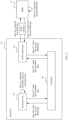
- the electronic device includes a processor 10 and a BMC 11.
- a communication interface is disposed between the processor 10 and the BMC 11.
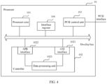
- the processor 10 includes a processor core 101 and at least one controller 102 ( FIG. 1 shows one controller 102, but is not limited to one controller 102).
- the communication interface disposed between the processor 10 and the BMC 11 may be a PCIE interface or an IPMB interface. Data may be transmitted between the processor 10 and the BMC 11 through the PCIE interface or the IPMB interface.
- the data transmitted between the processor 10 and the BMC 11 includes: first IPMI data sent by the processor 10 to the BMC 11, and second IPMI data sent by the BMC 11 to the processor 10.
- the first IPMI data is data that represents a status of the processor 10.
- the data that represents the status of the processor 10 may be an operating status parameter of each hardware device in the electronic device, for example, a parameter such as a temperature or a voltage.
- the processor core 101 In the data transmission process in which the processor 10 sends the first IPMI data to the BMC 11, the processor core 101 generates the first IPMI data in a running process, and sends the first PIMI data to the controller 102. After receiving the first IPMI data sent by the processor core 101, the controller 102 sends the first IPMI data to the BMC 11 through the PCIE interface or the IPMB interface.
- the BMC 11 is configured to: receive the first IPMI data, and manage the processor 10 based on the first IPMI data.
- the IPMI data may be transmitted through the PCIE interface or the IPMB interface disposed between the processor and the BMC.
- the processor 10 when the processor 10 and the BMC 11 perform data transmission through the PCIE interface, an optional implementation is that corresponding PCIE nodes are respectively disposed in the processor 10 and the BMC 11, to process data that needs to be transmitted through the PCIE interface.
- the processor 10 further includes a PCIE control unit 103 (for example, the PCIE control unit may be a PCIE root complex (Root Complex, RC)), and the PCIE control unit 103 in the processor 10 is mapped to a PCIE endpoint device (EndPoint, EP) in the BMC 11.
- the PCIE control unit 103 for example, the PCIE control unit may be a PCIE root complex (Root Complex, RC)
- the PCIE control unit 103 in the processor 10 is mapped to a PCIE endpoint device (EndPoint, EP) in the BMC 11.
- controller 102 may be further initialized. Steps of initializing the controller 102 in this embodiment of this application include:
- controllers may be disposed in the processor 10 in this embodiment of this application.
- One controller is configured to: process first IPMI data generated in the running process of the OS system, and process second IPMI data returned by the BMC 11 for the first IPMI data generated in the running process of the OS system.
- the other controller is configured to: process first IPMI data generated in the running process of the BIOS system, and process second IPMI data returned by the BMC 11 for the first IPMI data generated in the running process of the BIOS system.
- each controller corresponds to one interface register.
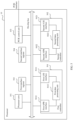
- FIG. 5 is a diagram of a structure of a processor.
- the processor 10 includes a processor core 101, a first controller 501, a second controller 502, a PCIE control unit 103, a first interface register 503 corresponding to the first controller 501, and a second interface register 504 corresponding to the second controller 502.
- the processor core 101, the first controller 501, the second controller 502, the PCIE control unit 103, the first interface register 503, and the second interface register 504 are connected through an on-chip bus.
- the first controller 501 and the first interface register 503 are configured to process IPMI data corresponding to an OS system.
- the IPMI data includes first IPMI data and/or second IPMI data.
- the second controller 502 and the second interface register 504 are configured to process IPMI data corresponding to a BIOS system.
- the IPMI data includes first IPMI data and/or second IPMI data.
- the first controller 501 includes a first AXI interface 5011, a first APB interface 5012, and a first data processing unit 5013.
- the second controller 502 includes a second AXI interface 5021, a second APB interface 5022, and a second data processing unit 5023.
- storage space that is in a BMC 11 and that is used to store the IPMI data corresponding to the OS system may be the same as or different from storage space that is used to store the IPMI data corresponding to the BIOS system.
- the processor core 101 allocates different storage space in the BMC 11 to the IPMI data corresponding to the OS system and the IPMI data corresponding to the BIOS system.
- the processor core 101 In a process in which the processor core 101 runs the OS system, if the processor core 101 generates first PIMI data, the processor core 101 writes the generated first PIMI data into the first interface register 503 through the on-chip bus.
- the first data processing unit 5013 in the first controller 501 obtains the first IPMI data from the first interface register 503 through the first AXI interface 5011 and the on-chip bus.
- the first data processing unit 5013 sends the first IPMI data to the PCIE control unit 103 through the first APB interface 5012.
- the PCIE control unit 103 stores, through the PCIE interface, the first IPMI data into the storage space that is in the BMC 11 and that is used to store the IPMI data corresponding to the OS system.
- the BMC 11 After the BMC 11 generates the second IPMI data returned for the first IPMI data corresponding to the OS system, the BMC 11 stores the second IPMI data into the storage space that is used to store the IPMI data corresponding to the OS system.
- the PCIE control unit 103 obtains the second IPMI data through the PCIE interface, and sends the second IPMI data to the first data processing unit 5013 through the first APB interface 5012.
- the first data processing unit 5013 writes the second IPMI data into the first interface register 503 through the first AXI interface 5011 and the on-chip bus.
- the processor core 101 obtains the second IPMI data from the first interface register 503 through the on-chip bus.
- the processor core 101 In a process in which the processor core 101 runs the BIOS system, if the processor core 101 generates first PIMI data, the processor core 101 writes the generated first PIMI data into the second interface register 504 through the on-chip bus.
- the second data processing unit 5023 in the second controller 502 obtains the first IPMI data from the second interface register 504 through the second AXI interface 5021 and the on-chip bus.
- the second data processing unit 5023 sends the first IPMI data to the PCIE control unit 103 b through the second APB interface 5022.
- the PCIE control unit 103 stores, through the PCIE interface, the first IPMI data into the storage space that is in the BMC 11 and that is used to store the IPMI data corresponding to the BIOS system.
- the BMC 11 After the BMC 11 generates the second IPMI data returned for the first IPMI data corresponding to the BIOS system, the BMC 11 stores the second IPMI data into the storage space that is used to store the IPMI data corresponding to the BIOS system.
- the PCIE control unit 103 obtains the second IPMI data through the PCIE interface, and sends the second IPMI data to the second data processing unit 5023 through the second APB interface 5022.
- the second data processing unit 5023 writes the second IPMI data into the second interface register 504 through the second AXI interface 5021 and the on-chip bus.
- the processor core 101 obtains the second IPMI data from the second interface register 504 through the on-chip bus.
- the following describes a method for transmitting data through the PCIE interface between the processor 10 and the BMC 11.
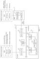
- FIG. 6 is a diagram of a structure of an electronic device.
- the electronic device includes a processor 10 and a BMC 11.
- a PCIE interface is disposed between the processor 10 and the BMC 11.
- the processor 10 includes a processor core 101, a BT controller 601, a PCIE control unit 103, and an interface register 104.
- the processor core 101, the BT controller 601, the PCIE control unit 103, and the interface register 104 are connected through an on-chip bus.
- the BT controller 601 further includes an AXI interface 6011, an APB interface 6012, and a data processing unit 6013.
- the BMC 11 includes a processing unit 111 and a storage unit 112.
- the processor core 101 processes generated IPMI data to obtain first PIMI data of an IPMI_BT type by invoking an IPMI BT protocol stack, and writes the first PIMI data into the interface register 104 through the on-chip bus.
- the data processing unit 6013 in the BT controller 601 obtains the first IPMI data from the interface register 104 through the AXI interface 6011 and the on-chip bus.
- the data processing unit 6013 sends the first IPMI data to the PCIE control unit 103 through the APB interface 6012.
- the PCIE control unit 103 stores, through the PCIE interface, the first IPMI data into storage space that is in the storage unit 112 of the BMC 11 and that corresponds to the PCIE interface.
- the processing unit 111 of the BMC 11 stores the second PIMI data into the storage space that is in the storage unit 112 and that corresponds to the PCIE interface.
- the PCIE control unit 103 obtains, through the PCIE interface, the second PIMI data from the storage space corresponding to the PCIE interface, and sends the second IPMI data to the data processing unit 6013 through the APB interface 6012.
- the data processing unit 6013 writes the second IPMI data into the interface register 104 through the AXI interface 6011 and the on-chip bus.
- the processor core 101 obtains the second IPMI data from the interface register 104 through the on-chip bus, and parses and processes the obtained second IPMI data by invoking an upper-layer IPMI BT protocol stack.
- FIG. 7 is a diagram of a structure of an electronic device.
- the electronic device includes a processor 10 and a BMC 11.
- a PCIE interface is disposed between the processor 10 and the BMC 11.
- the processor 10 includes a processor core 101, a KCS controller 701, a PCIE control unit 103, and an interface register 104.
- the processor core 101, the KCS controller 701, the PCIE control unit 103, and the interface register 104 are connected through an on-chip bus.
- the KCS controller 701 further includes an AXI interface 7011, an APB interface 7012, and a data processing unit 7013.
- the BMC 11 includes a processing unit 111 and a storage unit 112.
- the processor core 101 processes generated IPMI data to obtain first PIMI data of an IPMI_KCS type by invoking an IPMI KCS protocol stack, and writes the first PIMI data into the interface register 104 through the on-chip bus.
- the data processing unit 7013 in the KCS controller 701 obtains the first IPMI data from the interface register 104 through the AXI interface 7011 and the on-chip bus.
- the data processing unit 7013 sends the first IPMI data to the PCIE control unit 103 through the APB interface 7012.
- the PCIE control unit 103 stores, through the PCIE interface, the first IPMI data into storage space that is in the storage unit 112 of the BMC 11 and that corresponds to the PCIE interface.
- the processing unit 111 of the BMC 11 obtains the first PIMI data from the storage space corresponding to the PCIE interface, and parses the obtained first PIMI data by invoking a PCIE driver and a KCS driver in an upper-layer PIMI KCS protocol stack, to obtain IPMI-type data.
- the processing unit 111 of the BMC 11 stores the second PIMI data into the storage space that is in the storage unit 112 and that corresponds to the PCIE interface.
- the PCIE control unit 103 obtains, through the PCIE interface, the second PIMI data from the storage space corresponding to the PCIE interface, and sends the second IPMI data to the data processing unit 7013 through the APB interface 7012.
- the data processing unit 7013 writes the second IPMI data into the interface register 104 through the AXI interface 7011 and the on-chip bus.
- the processor core 101 obtains the second IPMI data from the interface register 104 through the on-chip bus, and parses and processes the obtained second IPMI data by invoking an upper-layer IPMI KCS protocol stack.
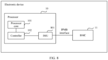
- an IMU is disposed in the processor 10, to process data that needs to be transmitted through the IPMB interface.
- the processor 10 includes an IMU 801.
- FIG. 10 is a diagram of a structure of a processor.
- the processor 10 includes a processor core 101, a controller 102, an IMU 801, and an interface register 104.
- the interface register 104 is a register based on a BT protocol, and is compatible with an IPMI BT protocol stack invoked in a running process of the processor core 101.
- the interface register 104 is a register based on a KCS protocol, and is compatible with an IPMI KCS protocol stack invoked in the running process of the processor core 101.
- Step 904 The IMU 801 sends the first IPMI data to the BMC 11 through an IPMB interface.
- the IMU 801 sends the first IPMI data to the BMC 11
- the IMU 801 sends the first IPMI data to the BMC 11 through the IPMB interface.
- Step 905 The BMC 11 generates second IPMI data for managing the processor 10.
- the BMC 11 may learn of a current status of the processor based on the first IPMI data, and may obtain, through analysis, a working status of a hardware device in the electronic device based on the first PIMI data.
- the BMC 11 generates, based on the working status of the hardware device in the electronic device, a control instruction for managing the processor 10, to adjust the working status of the hardware device in the electronic device by managing the processor 10.
- the BMC 11 generates the control instruction for managing the processor 10, and sends the generated control instruction as the second IPMI data to the processor 10.
- Step 906 The BMC 11 sends the second IPMI data to the IMU 801 through the IPMB interface.
- Step 907 The IMU 801 sends the second IPMI data to the controller 102.
- the IMU 801 When the IMU 801 sends the second IPMI data to the controller 102, based on the diagram of the structure of the processor shown in FIG. 10 , the IMU 801 transmits the second IPMI data to the AXI interface 1021 through the on-chip bus, and sends the second IPMI data to the data processing unit 1023 in the controller 102 through the AXI interface 1021.
- Step 908 The controller 102 sends the second IPMI data to the processor core 101.
- the data processing unit 1023 transmits the second IPMI data to the APB interface 1022, and writes the second IPMI data into the interface register 104 through the APB interface 1022 and the on-chip bus.
- the processor core 101 obtains the second IPMI data from the interface register 104 through the on-chip bus.
- the processor core 101 after receiving the second IPMI data sent by the BMC 11, the processor core 101 adjusts the status of the processor 10.
- a manner of adjusting the status of the processor 10 includes but is not limited to adjusting some operating parameters of the processor 10, or adjusting an operating parameter of another hardware device connected to the processor 10, to adjust the status of the processor 10.
- the processor core 101 generates the first IPMI data in the running process of the OS system or the BIOS system, and needs to send the generated first IPMI data to the BMC 11 by using the controller 102. If the BIOS system may simultaneously run in the running process of the OS system, when first IPMI data is simultaneously generated in the running processes of the OS system and the BIOS system, the processor core 101 needs to transmit, by using the controller 102, the first IPMI data simultaneously generated in the running processes of the OS system and the BIOS system. As a result, a use conflict of the controller 102 occurs.
- controllers may be disposed in the processor 10 in this embodiment of this application.
- One controller is configured to: process first IPMI data generated in the running process of the OS system, and process second IPMI data returned by the BMC 11 for the first IPMI data generated in the running process of the OS system.
- the other controller is configured to: process first IPMI data generated in the running process of the BIOS system, and process second IPMI data returned by the BMC 11 for the first IPMI data generated in the running process of the BIOS system.
- each controller corresponds to one interface register.
- the BMC 11 After the BMC 11 generates the second IPMI data returned for the first IPMI data corresponding to the OS system, the BMC 11 sends the second IPMI data to the IMU 801.
- the IMU 801 receives the second IPMI data through the IPMB interface, and sends the second IPMI data to the first data processing unit 5013 through the first APB interface 5012.
- the first data processing unit 5013 writes the second IPMI data into the first interface register 503 by using the first AXI interface 5011 and the on-chip bus.
- the processor core 101 obtains the second IPMI data from the first interface register 503 through the on-chip bus.
- the processor core 101 In a process in which the processor core 101 runs a BIOS system, if the processor core 101 generates first PIMI data, the processor core 101 writes the generated first PIMI data into the second interface register 504 through the on-chip bus.
- the second data processing unit 5023 in the second controller 502 obtains the first IPMI data from the second interface register 504 through the second AXI interface 5021 and the on-chip bus.
- the second data processing unit 5023 sends the first IPMI data to the IMU 801 through the second APB interface 5022.
- the IMU 801 sends the first IPMI data to the BMC 11 through an IPMB interface.
- the BMC 11 After the BMC 11 generates the second IPMI data returned for the first IPMI data corresponding to the BIOS system, the BMC 11 sends the second IPMI data to the IMU 801.
- the IMU 801 obtains the second IPMI data through the IPMB interface, and sends the second IPMI data to the second data processing unit 5023 through the second APB interface 5022.
- the second data processing unit 5023 writes the second IPMI data into the second interface register 504 through the second AXI interface 5021 and the on-chip bus.
- the processor core 101 obtains the second IPMI data from the second interface register 504 through the on-chip bus.
- the following describes a method for transmitting data through the IPMB interface between the processor 10 and the BMC 11.
- FIG. 12 is a diagram of a structure of an electronic device.
- the electronic device includes a processor 10 and a BMC 11.
- An IPMB interface is disposed between the processor 10 and the BMC 11.
- the processor 10 includes a processor core 101, a BT controller 601, an IMU 801, and an interface register 104.
- the processor core 101, the BT controller 601, the IMU 801, and the interface register 104 are connected through an on-chip bus.
- the BT controller 601 further includes an AXI interface 6011, an APB interface 6012, and a data processing unit 6013.
- the BMC 11 includes a processing unit 111.
- the processor core 101 processes generated IPMI data to obtain first PIMI data of an IPMI_BT type by invoking an IPMI BT protocol stack, and writes the first PIMI data into the interface register 104 through the on-chip bus.
- the data processing unit 6013 in the BT controller 601 obtains the first IPMI data from the interface register 104 through the AXI interface 6011 and the on-chip bus.
- the data processing unit 6013 sends the first IPMI data to the IMU 801 through the APB interface 6012.
- the IMU 801 sends the first IPMI data to the processing unit 111 of the BMC 11 through the IPMB interface.
- the processing unit 111 of the BMC 11 parses the obtained first PIMI data by invoking an IPMB driver (Driver) and a BT driver in an upper-layer PIMI BT protocol stack, to obtain IPMI-type data.
- IPMB driver Driver
- BT driver BT driver
- the processing unit 111 of the BMC 11 sends the second PIMI data to the IMU 801.
- the IMU 801 sends the second IPMI data to the data processing unit 6013 through the APB interface 6012.
- the data processing unit 6013 writes the second IPMI data into the interface register 104 through the AXI interface 6011 and the on-chip bus.
- the processor core 101 obtains the second IPMI data from the interface register 104 through the on-chip bus, and parses and processes the obtained second IPMI data by invoking an upper-layer IPMI BT protocol stack.
- FIG. 13 is a diagram of a structure of an electronic device.
- the electronic device includes a processor 10 and a BMC 11.
- An IPMB interface is disposed between the processor 10 and the BMC 11.
- the processor 10 includes a processor core 101, a KCS controller 701, an IMU 801, and an interface register 104.
- the processor core 101, the KCS controller 701, the IMU 801, and the interface register 104 are connected through an on-chip bus.
- the KCS controller 701 further includes an AXI interface 7011, an APB interface 7012, and a data processing unit 7013.
- the BMC 11 includes a processing unit 111.
- the first transceiver unit 1401 is specifically configured to: send the first IPMI data to an IMU in the processor, so that the IMU sends the first IPMI data to the BMC through the IPMB interface.
- the computer instructions may be transmitted from a website, computer, server, or data center to another website, computer, server, or data center in a wired (for example, a coaxial cable, an optical fiber, or a digital subscriber line (DSL)) or wireless (for example, infrared, radio, or microwave) manner.
- the computer-readable storage medium may be any usable medium accessible by a computer, or a data storage device, such as a server or a data center, integrating one or more usable media.
- the usable medium may be a magnetic medium (for example, a floppy disk, a hard disk, or a magnetic tape), an optical medium (for example, a DVD), or a semiconductor medium.
- the semiconductor medium may be a solid-state drive (solid-state drive, SSD).
- this application may be provided as a method, a system, or a computer program product. Therefore, this application may use a form of hardware only embodiments, software only embodiments, or embodiments with a combination of software and hardware. In addition, this application may use a form of a computer program product that is implemented on one or more computer-usable storage media (including but not limited to a disk memory, a CD-ROM, an optical memory, and the like) that include computer-usable program code.
- computer-usable storage media including but not limited to a disk memory, a CD-ROM, an optical memory, and the like
- These computer program instructions may be provided for a general-purpose computer, a dedicated computer, an embedded processor, or a processor of any other programmable data processing device to generate a machine, so that the instructions executed by a computer or a processor of any other programmable data processing device generate an apparatus for implementing a specific function in one or more processes in the flowcharts and/or in one or more blocks in the block diagrams.
- These computer program instructions may be stored in a computer-readable memory that can instruct the computer or any other programmable data processing device to work in a specific manner, so that the instructions stored in the computer-readable memory generate an artifact that includes an instruction apparatus.
- the instruction apparatus implements a specific function in one or more processes in the flowcharts and/or in one or more blocks in the block diagrams.
- the computer program instructions can alternatively be loaded onto a computer or another programmable data processing device, so that a series of operations and steps are performed on the computer or the another programmable device to generate computer-implemented processing. Therefore, the instructions executed on the computer or the another programmable device provide steps for implementing a specific function in one or more procedures in the flowcharts and/or in one or more blocks in the block diagrams.
Landscapes
- Engineering & Computer Science (AREA)
- Theoretical Computer Science (AREA)
- General Engineering & Computer Science (AREA)
- Physics & Mathematics (AREA)
- General Physics & Mathematics (AREA)
- Computer Hardware Design (AREA)
- Computing Systems (AREA)
- Quality & Reliability (AREA)
- Mathematical Physics (AREA)
- Microelectronics & Electronic Packaging (AREA)
- Information Transfer Systems (AREA)
- Computer And Data Communications (AREA)
Applications Claiming Priority (2)
| Application Number | Priority Date | Filing Date | Title |
|---|---|---|---|
| CN202211174451.8A CN117807003A (zh) | 2022-09-26 | 2022-09-26 | 一种电子设备、处理器、数据传输方法及装置 |
| PCT/CN2023/115348 WO2024066857A1 (fr) | 2022-09-26 | 2023-08-28 | Dispositif électronique, processeur et procédé et appareil de transmission de données |
Publications (2)
| Publication Number | Publication Date |
|---|---|
| EP4582964A1 true EP4582964A1 (fr) | 2025-07-09 |
| EP4582964A4 EP4582964A4 (fr) | 2025-12-31 |
Family
ID=90422236
Family Applications (1)
| Application Number | Title | Priority Date | Filing Date |
|---|---|---|---|
| EP23870100.7A Pending EP4582964A4 (fr) | 2022-09-26 | 2023-08-28 | Dispositif électronique, processeur et procédé et appareil de transmission de données |
Country Status (4)
| Country | Link |
|---|---|
| US (1) | US20250225094A1 (fr) |
| EP (1) | EP4582964A4 (fr) |
| CN (1) | CN117807003A (fr) |
| WO (1) | WO2024066857A1 (fr) |
Families Citing this family (1)
| Publication number | Priority date | Publication date | Assignee | Title |
|---|---|---|---|---|
| US12688046B2 (en) * | 2024-11-05 | 2026-07-21 | Dell Products L.P. | BIOS/BMC initialization communication system |
Family Cites Families (24)
| Publication number | Priority date | Publication date | Assignee | Title |
|---|---|---|---|---|
| US7069349B2 (en) * | 2002-01-10 | 2006-06-27 | Intel Corporation | IPMI dual-domain controller |
| US9025586B2 (en) * | 2007-09-21 | 2015-05-05 | Texas Instruments Incorporated | Secondary synchronization signal mapping |
| US9384018B2 (en) * | 2012-07-27 | 2016-07-05 | Vmware, Inc. | Virtual intelligent platform management interface for hardware components |
| US9043527B2 (en) * | 2013-01-04 | 2015-05-26 | American Megatrends, Inc. | PCI express channel implementation in intelligent platform management interface stack |
| US9367419B2 (en) * | 2013-01-08 | 2016-06-14 | American Megatrends, Inc. | Implementation on baseboard management controller of single out-of-band communication access to multiple managed computer nodes |
| US9331899B2 (en) * | 2013-03-13 | 2016-05-03 | American Megatrends, Inc. | Scalable BMC management stacks using virtual networks on single physical network device |
| WO2015177879A1 (fr) * | 2014-05-20 | 2015-11-26 | 富士通株式会社 | Dispositif de traitement d'informations, système de traitement d'informations et procédé |
| CN104202195B (zh) * | 2014-09-10 | 2018-05-04 | 华为技术有限公司 | 服务器统一通信的方法、基板管理控制器和服务器 |
| CN104378237A (zh) * | 2014-11-24 | 2015-02-25 | 英业达科技有限公司 | 判定服务节点状态的方法 |
| CN105893293B (zh) * | 2014-12-18 | 2019-10-29 | 伊姆西公司 | 用于管理外部组件快速互连设备热插拔的系统和方法 |
| US9729440B2 (en) * | 2015-02-22 | 2017-08-08 | Mellanox Technologies, Ltd. | Differentiating among multiple management control instances using IP addresses |
| US9916270B2 (en) * | 2015-03-27 | 2018-03-13 | Intel Corporation | Virtual intelligent platform management interface (IPMI) satellite controller and method |
| US10069718B2 (en) * | 2015-11-26 | 2018-09-04 | Dell Products, L.P. | Switching of host network traffic through baseboard management controller (BMC) |
| US9940143B2 (en) * | 2016-03-17 | 2018-04-10 | Dell Products, L.P. | Using peripheral component interconnect express vendor-defined message (PCIe-VDM) and inter-integrated circuit (I2C) transport for network communications |
| TWI604304B (zh) * | 2016-03-28 | 2017-11-01 | 緯創資通股份有限公司 | 電子裝置及其檢測方法 |
| US10050907B2 (en) * | 2016-06-13 | 2018-08-14 | Dell Products, Lp | Virtual PCIe based ethernet controller for in-band communication between server and BMC |
| US10210842B2 (en) * | 2017-02-07 | 2019-02-19 | American Megatrends, Inc. | Techniques of displaying host data on a monitor connected to a service processor during pre-boot initialization stage |
| US10958990B2 (en) * | 2017-05-03 | 2021-03-23 | Intel Corporation | Trusted platform telemetry mechanisms inaccessible to software |
| US11194588B2 (en) * | 2018-07-09 | 2021-12-07 | Dell Products L.P. | Information handling systems and method to provide secure shared memory access at OS runtime |
| US11442885B2 (en) * | 2019-08-09 | 2022-09-13 | Dell Products L.P. | System and method to change field-programmable gate array personality from a baseboard management controller |
| CN110532150B (zh) * | 2019-08-23 | 2023-01-10 | 苏州浪潮智能科技有限公司 | 一种机箱管理方法、装置、存储介质及处理器 |
| US11243589B1 (en) * | 2019-09-24 | 2022-02-08 | Amazon Technologies, Inc. | Remote power button actuation device for a pre-assembled computer system integrated into a server for a virtualization service |
| CN112838952B (zh) * | 2021-01-04 | 2022-05-31 | 联想(北京)有限公司 | 基板管理控制器的数据传输方法、bmc、服务器和介质 |
| CN114116378B (zh) * | 2021-11-11 | 2023-12-22 | 苏州浪潮智能科技有限公司 | 获取PCIe设备温度的方法、系统、终端及存储介质 |
-
2022
- 2022-09-26 CN CN202211174451.8A patent/CN117807003A/zh active Pending
-
2023
- 2023-08-28 EP EP23870100.7A patent/EP4582964A4/fr active Pending
- 2023-08-28 WO PCT/CN2023/115348 patent/WO2024066857A1/fr not_active Ceased
-
2025
- 2025-03-25 US US19/089,279 patent/US20250225094A1/en active Pending
Also Published As
| Publication number | Publication date |
|---|---|
| US20250225094A1 (en) | 2025-07-10 |
| CN117807003A (zh) | 2024-04-02 |
| WO2024066857A1 (fr) | 2024-04-04 |
| EP4582964A4 (fr) | 2025-12-31 |
Similar Documents
| Publication | Publication Date | Title |
|---|---|---|
| US11061837B2 (en) | UBM implementation inside BMC | |
| CN104579772B (zh) | 计算机设备与计算机设备的配置管理方法 | |
| EP3255527B1 (fr) | Technologies clavier-vidéo-souris à distance | |
| CN110554943B (zh) | 一种基于i3c的多节点服务器cmc管理系统及方法 | |
| US9430266B2 (en) | Activating a subphysical driver on failure of hypervisor for operating an I/O device shared by hypervisor and guest OS and virtual computer system | |
| US9026687B1 (en) | Host based enumeration and configuration for computer expansion bus controllers | |
| US10996942B1 (en) | System and method for graphics processing unit firmware updates | |
| CN117251039A (zh) | 设备复位方法、装置、存储介质及电子设备 | |
| WO2023160699A1 (fr) | Système, procédé et appareil de gestion de carte unique, et dispositif | |
| CN116541227A (zh) | 故障诊断方法、装置、存储介质、电子装置及bmc芯片 | |
| EP4592833A1 (fr) | Procédé d'exécution de système de contrôleur de gestion de carte de base, et contrôleur de gestion de carte de base | |
| CN119336668B (zh) | 网卡的管理方法及装置 | |
| US20260119248A1 (en) | Method and apparatus of distributed resource management, system, device, and storage medium | |
| US20250225094A1 (en) | Electronic device, processor, and data transmission method and apparatus | |
| EP3968170A1 (fr) | Procédé et appareil de gestion de dispositif intelligent, dispositif réseau et support de stockage lisible | |
| US12487959B2 (en) | Enabling out-of-band generic PCIe switch control/configuration management using BMC for dynamic, scalable hardware requirements | |
| CN120743662A (zh) | 一种测试板及测试系统 | |
| CN117041184B (zh) | Io拓展装置及io交换机 | |
| CN104081369A (zh) | 在预引导环境中建立模块化节点的连接性 | |
| US11061838B1 (en) | System and method for graphics processing unit management infrastructure for real time data collection | |
| CN119576598B (zh) | 一种基于连接器的端口管理方法及相关设备 | |
| WO2024174947A1 (fr) | Procédé et appareil de branchement à chaud, et dispositif informatique | |
| CN116521574A (zh) | 一种存储模块的信息获取方法以及相关装置 | |
| CN112579507A (zh) | 宿主机与bmc通信的方法、bios、操作系统、bmc和服务器 | |
| CN114857069B (zh) | 一种风扇治具板 |
Legal Events
| Date | Code | Title | Description |
|---|---|---|---|
| STAA | Information on the status of an ep patent application or granted ep patent |
Free format text: STATUS: THE INTERNATIONAL PUBLICATION HAS BEEN MADE |
|
| PUAI | Public reference made under article 153(3) epc to a published international application that has entered the european phase |
Free format text: ORIGINAL CODE: 0009012 |
|
| STAA | Information on the status of an ep patent application or granted ep patent |
Free format text: STATUS: REQUEST FOR EXAMINATION WAS MADE |
|
| 17P | Request for examination filed |
Effective date: 20250401 |
|
| AK | Designated contracting states |
Kind code of ref document: A1 Designated state(s): AL AT BE BG CH CY CZ DE DK EE ES FI FR GB GR HR HU IE IS IT LI LT LU LV MC ME MK MT NL NO PL PT RO RS SE SI SK SM TR |
|
| A4 | Supplementary search report drawn up and despatched |
Effective date: 20251201 |
|
| DAV | Request for validation of the european patent (deleted) | ||
| DAX | Request for extension of the european patent (deleted) | ||
| RIC1 | Information provided on ipc code assigned before grant |
Ipc: G06F 13/38 20060101AFI20251125BHEP Ipc: G06F 11/30 20060101ALI20251125BHEP Ipc: G06F 13/12 20060101ALI20251125BHEP Ipc: G06F 13/42 20060101ALI20251125BHEP Ipc: G06F 11/34 20060101ALI20251125BHEP Ipc: G06F 13/40 20060101ALI20251125BHEP Ipc: H04L 41/0681 20220101ALI20251125BHEP Ipc: H04L 43/0817 20220101ALI20251125BHEP |