EP4583659A2 - Dispositifs ayant un transistor et un condensateur le long d'un niveau horizontal commun, et procédés de formation de dispositifs - Google Patents
Dispositifs ayant un transistor et un condensateur le long d'un niveau horizontal commun, et procédés de formation de dispositifs Download PDFInfo
- Publication number
- EP4583659A2 EP4583659A2 EP25176032.8A EP25176032A EP4583659A2 EP 4583659 A2 EP4583659 A2 EP 4583659A2 EP 25176032 A EP25176032 A EP 25176032A EP 4583659 A2 EP4583659 A2 EP 4583659A2
- Authority
- EP
- European Patent Office
- Prior art keywords
- levels
- transistor
- assembly
- insulative
- along
- Prior art date
- Legal status (The legal status is an assumption and is not a legal conclusion. Google has not performed a legal analysis and makes no representation as to the accuracy of the status listed.)
- Pending
Links
Images


Classifications
-
- H—ELECTRICITY
- H10—SEMICONDUCTOR DEVICES; ELECTRIC SOLID-STATE DEVICES NOT OTHERWISE PROVIDED FOR
- H10B—ELECTRONIC MEMORY DEVICES
- H10B12/00—Dynamic random access memory [DRAM] devices
- H10B12/30—DRAM devices comprising one-transistor - one-capacitor [1T-1C] memory cells
-
- H—ELECTRICITY
- H10—SEMICONDUCTOR DEVICES; ELECTRIC SOLID-STATE DEVICES NOT OTHERWISE PROVIDED FOR
- H10B—ELECTRONIC MEMORY DEVICES
- H10B12/00—Dynamic random access memory [DRAM] devices
- H10B12/01—Manufacture or treatment
- H10B12/02—Manufacture or treatment for one transistor one-capacitor [1T-1C] memory cells
- H10B12/03—Making the capacitor or connections thereto
-
- H—ELECTRICITY
- H10—SEMICONDUCTOR DEVICES; ELECTRIC SOLID-STATE DEVICES NOT OTHERWISE PROVIDED FOR
- H10B—ELECTRONIC MEMORY DEVICES
- H10B12/00—Dynamic random access memory [DRAM] devices
- H10B12/01—Manufacture or treatment
- H10B12/02—Manufacture or treatment for one transistor one-capacitor [1T-1C] memory cells
- H10B12/05—Making the transistor
-
- H—ELECTRICITY
- H10—SEMICONDUCTOR DEVICES; ELECTRIC SOLID-STATE DEVICES NOT OTHERWISE PROVIDED FOR
- H10B—ELECTRONIC MEMORY DEVICES
- H10B12/00—Dynamic random access memory [DRAM] devices
- H10B12/30—DRAM devices comprising one-transistor - one-capacitor [1T-1C] memory cells
- H10B12/48—Data lines or contacts therefor
- H10B12/482—Bit lines
-
- H—ELECTRICITY
- H10—SEMICONDUCTOR DEVICES; ELECTRIC SOLID-STATE DEVICES NOT OTHERWISE PROVIDED FOR
- H10B—ELECTRONIC MEMORY DEVICES
- H10B12/00—Dynamic random access memory [DRAM] devices
- H10B12/30—DRAM devices comprising one-transistor - one-capacitor [1T-1C] memory cells
- H10B12/48—Data lines or contacts therefor
- H10B12/485—Bit line contacts
-
- H—ELECTRICITY
- H10—SEMICONDUCTOR DEVICES; ELECTRIC SOLID-STATE DEVICES NOT OTHERWISE PROVIDED FOR
- H10B—ELECTRONIC MEMORY DEVICES
- H10B12/00—Dynamic random access memory [DRAM] devices
- H10B12/30—DRAM devices comprising one-transistor - one-capacitor [1T-1C] memory cells
- H10B12/48—Data lines or contacts therefor
- H10B12/488—Word lines
-
- G—PHYSICS
- G11—INFORMATION STORAGE
- G11C—STATIC STORES
- G11C2211/00—Indexing scheme relating to digital stores characterized by the use of particular electric or magnetic storage elements; Storage elements therefor
- G11C2211/56—Indexing scheme relating to G11C11/56 and sub-groups for features not covered by these groups
- G11C2211/561—Multilevel memory cell aspects
-
- H—ELECTRICITY
- H10—SEMICONDUCTOR DEVICES; ELECTRIC SOLID-STATE DEVICES NOT OTHERWISE PROVIDED FOR
- H10B—ELECTRONIC MEMORY DEVICES
- H10B12/00—Dynamic random access memory [DRAM] devices
-
- H—ELECTRICITY
- H10—SEMICONDUCTOR DEVICES; ELECTRIC SOLID-STATE DEVICES NOT OTHERWISE PROVIDED FOR
- H10W—GENERIC PACKAGES, INTERCONNECTIONS, CONNECTORS OR OTHER CONSTRUCTIONAL DETAILS OF DEVICES COVERED BY CLASS H10
- H10W90/00—Package configurations
Definitions
- the DRAM unit cells may each comprise a capacitor in combination with a transistor. Charge stored on the capacitors of the DRAM unit cells may correspond to memory bits.
- Some embodiments include integrated devices having capacitors and transistors, with the capacitors being horizontally offset from the transistors.
- the integrated devices may be vertically stacked one atop another in an integrated assembly.
- the integrated devices may be memory cells of a DRAM array.
- Some embodiments include methods of forming integrated devices which have capacitors horizontally offset from transistors, and some embodiments include methods of forming architectures which comprise vertically-stacked tiers of such integrated devices. Example embodiments are described with reference to FIGS. 1-23 .
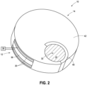
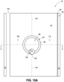
- a device 10 is illustrated to comprise a transistor 12 and a capacitor 14.
- the transistor 12 includes a gate 16, and a semiconductor material 18 adjacent the gate.
- the semiconductor material 18 includes a channel region 17.
- the channel region 17 is not visible in FIG. 1 , as it is under a portion of the gate 16; but an approximate location of the channel region is diagrammatically illustrated with a dashed arrow.
- the semiconductor material 18 also includes a first source/drain region 19 on one side of the channel region 17, and a second source/drain region 21 on an opposing side of the channel region from the first source/drain region 19.
- the transistor gate 16 comprises conductive material 20.
- conductive material may comprise any suitable electrically conductive composition(s), such as, for example, one or more of various metals (e.g., titanium, tungsten, cobalt, nickel, platinum, ruthenium, etc.), metal-containing compositions (e.g., metal silicide, metal nitride, metal carbide, etc.), and/or conductively-doped semiconductor materials (e.g., conductively-doped silicon, conductively-doped germanium, etc.).
- various metals e.g., titanium, tungsten, cobalt, nickel, platinum, ruthenium, etc.
- metal-containing compositions e.g., metal silicide, metal nitride, metal carbide, etc.
- conductively-doped semiconductor materials e.g., conductively-doped silicon, conductively-doped germanium, etc.
- the semiconductor material 18 may comprise any suitable composition or combination of compositions; such as, for example, one or more of silicon, germanium, III/V materials (e.g., gallium phosphide), semiconductor oxides, etc.
- the source/drain regions 19 and 21 may comprise conductively-doped regions.
- the channel region 17 may be doped to an appropriate level to achieve a desired threshold voltage.
- the capacitor 14 comprises a first electrode 22 and a second electrode 24.
- the electrodes 22 and 24 are spaced from one another, and dielectric material would be between the first and second electrodes.
- the dielectric material is not shown in FIG. 1 in order to simplify the drawing, but would be similar to the dielectric material 128 described below with reference to FIG. 23 .
- the electrodes 22 and 24 comprise conductive materials 28 and 30, respectively.
- Such conductive materials may comprise any suitable electrically conductive composition(s), such as, for example, one or more of various metals (e.g., titanium, tungsten, cobalt, nickel, platinum, ruthenium, etc.), metal-containing compositions (e.g., metal silicide, metal nitride, metal carbide, etc.), and/or conductively-doped semiconductor materials (e.g., conductively-doped silicon, conductively-doped germanium, etc.).
- the conductive materials 28 and 30 may be the same as one another in some embodiments, and may be different from one another in other embodiments.
- the electrodes 22 and 24 may be respectively referred to as a bottom electrode and a top electrode, a storage node electrode and a plate electrode, a bottom plate and a top plate, etc.
- the second source/drain region 21 is coupled with the first electrode 22 of the capacitor 14; and in the illustrated embodiment is directly against the first electrode 22.
- a bitline 32 extends through the device 10, and is coupled with the first source/drain region 19. In the illustrated embodiment, the first source/drain region 19 is directly against the bitline 32.
- the bitline 32 comprises conductive material 34.
- the conductive material 34 may comprise any suitable electrically conductive composition(s), such as, for example, one or more of various metals (e.g., titanium, tungsten, cobalt, nickel, platinum, ruthenium, etc.), metal-containing compositions (e.g., metal silicide, metal nitride, metal carbide, etc.), and/or conductively-doped semiconductor materials (e.g., conductively-doped silicon, conductively-doped germanium, etc.).
- various metals e.g., titanium, tungsten, cobalt, nickel, platinum, ruthenium, etc.
- metal-containing compositions e.g., metal silicide, metal nitride, metal carbide, etc.
- conductively-doped semiconductor materials e.g., conductively-doped silicon, conductively-doped germanium, etc.
- a wordline 36 is coupled with the gate 12.
- the device 10 may correspond to a memory cell, and may be one of many memory cells of a memory array (for instance, a DRAM array).
- the memory cell 10 may be addressed (i.e., read from/written to) utilizing the wordline 36 and the bitline 32.
- the device 10 may comprise numerous insulative materials which are not shown in the diagram of FIG. 1 in order to simplify the drawing.
- the capacitor dielectric material i.e., the material 128 shown in FIG. 23
- gate dielectric material would be provided between the gate and the channel region 17 (example gate dielectric material is shown in FIG. 19 as material 38).
- insulative materials would be provided to surround the device 10, and to isolate the bitline 32 from the capacitor 14.
- FIG. 2 shows insulative material 40 provided between the bitline 32 and the capacitor 14, and shows insulative material 42 over the transistor 12 and the capacitor 14.
- the insulative materials 40 and 42 may comprise any suitable composition(s); and in some embodiments may comprise one or more of silicon dioxide, silicon nitride, high-k oxides (with high-k meaning a dielectric constant greater than that of silicon dioxide), etc.
- the insulative materials 40 and 42 may be the same composition as one another in some embodiments, and may be different compositions relative to one another in other embodiments. Further, in some embodiments either or both of the materials 40 and 42 may comprise two or more different materials, rather than the single homogeneous materials illustrated in FIG. 2 .
- the bitline 32 may have a different configuration than shown in FIG. 1 .
- FIG. 1 shows the bitline 32 configured to be substantially circular along a horizontal cross-section through the bitline.
- the bitline may be polygonal, square, rectangular, elliptical, etc.
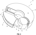
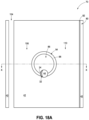
- FIG. 3 shows a configuration in which the bitline 32 is crescent-shaped along a horizontal cross-section through the bitline.
- the crescent-shaped bitline is along an insulative material 44.
- Such insulative material may comprise, for example, any of the compositions discussed above with reference to FIG. 2 for the insulative materials 40 and 42.
- the insulative material 44 may be the same as one or both of the insulative materials 40 and 42.
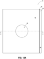
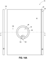
- the devices 10 of FIGS. 1-5 have the capacitor 14 horizontally-offset relative to the transistor 12. Also, all of the devices are substantially circular along horizontal cross-sections through the devices (with the term "substantially circular” meaning circular to within reasonable tolerances of fabrication and measurement). The devices may have other shapes in other embodiments, as discussed in more detail below with reference to FIG. 8 .
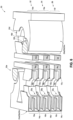
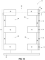
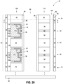
- FIG. 6 shows an example memory array 50 comprising memory cells 10a-f having the configuration of the device 10 of FIG. 1 .
- Each memory cell comprises a capacitor (e.g., the capacitors 14a-c visible in FIG. 6 ) coupled with an associated transistor (e.g., the transistors 12a-12c visible in FIG. 6 ).
- the capacitors are vertically-stacked one atop another along levels 52, 54 and 56.
- the level 52 comprises the memory cells 10a and 10d;
- the level 54 comprises the memory cells 10b and 10e;
- the level 56 comprises the memory cells 10c and 10f.
- Insulative materials are not shown in FIG. 6 in order to simplify the drawing, but it is to be understood that insulative materials analogous those described above with reference to FIGS. 1 and 2 (e.g., capacitor dielectric material, gate dielectric material, etc.) would be provided.
- Wordlines (e.g., access lines, etc.) 36a-f extend horizontally, and are coupled with transistor gates of the memory cells 10a-f (the transistor gates are not labeled in FIG. 6 , but would be analogous to the transistor gate 16 of FIG. 1 ).
- Each memory cell 10a-f may be uniquely addressed through a combination of one of the digit lines (32a, 32b), and one of the wordlines (36a-f).
- the wordlines may be considered to extend along rows of the array of memory cells
- the digit lines may be considered to extend along columns of the array of memory cells.
- the memory cells within each level may be substantially identical to one another (with the term "substantially identical” meaning identical to within reasonable tolerances of fabrication and measurement). Further, at least some of the memory cells within one vertical level (e.g., level 52) may be substantially identical to memory cells within another vertical level (e.g., level 54). In some embodiments, all of the memory cells within one vertical level may be substantially identical to all of the memory cells within another vertical level. In some embodiments, all of the memory cells within all of the vertical levels may be substantially identical to one another.
- At least some of the memory cells within one vertical level may not be substantially identical to at least some of the memory cells within another vertical level. Such may enable different vertical levels to be tailored for different applications. Differences between the memory cells in one vertical level relative to the memory cells in another vertical level may provide different performance characteristics amongst transistors of the memory cells (such as, for example, differences in one or more of effective gate width, effective gate length, threshold voltage, on-current, off-current, etc.) and/or different performance characteristics amongst capacitors of the memory cells (such as, for example, differences in capacitance).
- differences in performance characteristics amongst transistors of the memory cells may be achieved by providing different semiconductor material within one level as compared to another level (e.g., the semiconductor material 18a may be different relative to the semiconductor material 18b); with the differences between the semiconductor materials being differences in composition, differences in thickness, and/or differences in any other suitable physical characteristics.
- differences in performance characteristics between one level and another may be achieved by providing different dopants and/or dopant concentrations within the semiconductor material of one level as compared to the semiconductor material of another level (e.g., by providing different dopant and/or dopant concentrations within the semiconductor material 18a as compared to the semiconductor material 18b).
- Differences in performance characteristics amongst capacitors of different levels may be achieved by, for example, forming the electrodes to be of different shapes amongst the capacitors, utilizing different materials for capacitor dielectric amongst the capacitors and/or by utilizing different thicknesses of capacitor dielectric amongst the capacitors.
- FIG. 7 shows another view of a region of the memory array 50, and shows a pair of adjacent rows 58 and 60 along the level 52. Insulative materials are not shown in FIG. 7 in order to simplify the drawing, but it is to be understood that insulative materials analogous those described above with reference to FIGS. 1 and 2 (e.g., capacitor dielectric material, gate dielectric material, etc.) would be provided.
- the row 58 comprises memory cells 10a, 10g and 10h; and the row 60 comprises memory cells 10d, 10i, 10j and 10k.
- the embodiment of FIG. 7 illustrates one example arrangement of digit lines (32a-f), and wordlines (36a and 36d) relative to the memory cells. Other arrangements may be utilized in other embodiments.
- FIGS. 1-7 are illustrated to be substantially circular along horizontal cross-sections through the memory cells, it is to be understood that in other embodiments the memory cells may have other configurations.
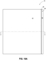
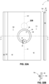
- FIG. 8 shows a top view of a memory cell 10 in a configuration in which the memory cell has a polygonal shape along a horizontal cross-section through the memory cell.
- the memory cell is substantially square along the horizontal cross-section through the memory cell.
- the memory cell may have any other suitable shape.
- the devices 10 of FIGS. 1-8 may be fabricated with any suitable processing.
- the devices are fabricated by providing holes through a stack of materials.
- the transistors are formed along a side of the holes, and the capacitors are formed along other sides of the holes.
- FIG. 9 shows a top view of a construction 62 illustrating example locations 64 for holes 86 (only some which are labeled) utilized during fabrication devices.
- the holes 86 are lined with a material 96, which is described in more detail below with reference to FIG. 13 .
- FIG. 9 also shows locations 66 where slits will be formed for fabrication of the transistor gates and wordlines, and shows locations 68 where slits will be formed for fabrication of the capacitors.
- FIG. 9 is provided to provide the reader with an overview of an example method for fabricating an array of devices (e.g., the example devices 10 of FIGS. 1-8 ) in accordance with an example embodiment.
- the devices may be fabricated utilizing other constructions.
- FIGS. 10-23 and 10A-23A An example method for fabricating devices analogous to the device 10 of FIG. 3 is described with reference to FIGS. 10-23 and 10A-23A .
- the views of FIGS. 10A-23A are along the cross-sections Z-Z of FIGS. 10-23 , respectively; and the views of FIGS. 10-23 are along the lines X-X of FIGS. 10A-23A , respectively. It is to be understood that the example method of FIGS. 10-23 and 10A-23A may be modified to fabricate any of the devices of FIGS. 1-8 , or analogous devices.
- an assembly 70 comprises a stack 72 of first levels 74 and second levels 76.
- the levels 74 and 76 alternate with one another along a vertical direction.
- the second levels 76 may be referred to as device levels, since integrated devices are eventually formed within the second levels 76.
- the stack 72 is supported by a base 84.
- the base 84 may comprise semiconductor material; and may, for example, comprise, consist essentially of, or consist of monocrystalline silicon.
- the base 84 may be referred to as a semiconductor substrate.
- semiconductor substrate means any construction comprising semiconductive material, including, but not limited to, bulk semiconductive materials such as a semiconductive wafer (either alone or in assemblies comprising other materials), and semiconductive material layers (either alone or in assemblies comprising other materials).
- substrate refers to any supporting structure, including, but not limited to, the semiconductor substrates described above.
- the base 84 may correspond to a semiconductor substrate containing one or more materials associated with integrated circuit fabrication. Such materials may include, for example, one or more of refractory metal materials, barrier materials, diffusion materials, insulator materials, etc.
- an opening 86 is formed through the stack 72.
- the opening 86 may be referred to as a first opening, and may be representative of a plurality of openings formed through the stack 74 (a plurality of openings 86 is shown in FIG. 9 , and discussed above). Only a single opening 86 is shown in the views of FIGS. 11 and 11A in order to simplify the drawings, but it is to be understood that such opening may be one of a large number of substantially identical openings formed through the stack.
- sacrificial materials 90 and 92 are formed within the cavities 88, and then an insulative liner 94 is formed along a peripheral boundary of the opening 86.
- a layer of the first material 92 is provided between a pair of layers of the second material 90 within each of the cavities 88.
- the liner 94 comprises an insulative material 96.
- the material 96 may comprise any suitable composition or combination of compositions; and in some embodiments may comprise, consist essentially of, or consist of silicon nitride.
- construction 70 is shown at a processing stage subsequent to that of FIG. 13A .
- a second opening 98 is formed overlapping a region of the first opening 86, and the second opening 98 is filled with a digit line template 100.
- the digit line template 100 extends vertically through the stack 72.
- the digit line template comprises two materials 44 and 102.
- the material 44 may comprise any of the insulative compositions described above with reference to FIG. 3 .
- the material 102 is a sacrificial material, and in some embodiments may comprise, consist essentially of, or consist of phosphosilicate glass.
- the illustrated digit line template 100 comprising the two materials 44 and 102 will ultimately form a digit line 32 having the configuration shown in FIG.
- the digit line template 100 may comprise only the sacrificial material 102, and may be utilized to form a digit line 32 having the configuration shown in FIG. 1 as being circular shaped along a horizontal cross-section.
- the sacrificial material 102 may be in any other suitable shape for forming a desired digit line configuration.
- the sacrificial material 92 is removed from along the slit 104 to form horizontally-extending voids 108. Such removal may be accomplished by passing appropriate etchant into the slit 104, and utilizing a timed etch to remove a desired amount of the sacrificial material 92.
- the voids 108 may be formed to extend about halfway around opening 86. Such is diagrammatically illustrated in the top view of FIG. 15A utilizing a dashed line 107 to illustrate approximate lateral boundaries (i.e., edges) of the voids 108 within the stack 72.
- the sacrificial material 102 of the digit line template 100 may comprise a same composition as the sacrificial material 92 (e.g., both may comprise phosphosilicate glass). Accordingly, the sacrificial material 102 of the digit line template 100 may be removed simultaneously with the removal of the sacrificial material 92 to leave a void 103.
- semiconductor material 18 is provided within the horizontally-extending voids 108 ( FIG. 15 ), and such semiconductor material replaces the sacrificial material 92 which had been removed to form such voids.
- the semiconductor material 18 may abut the sacrificial material 92 along the edges of the previous voids 108 (with such edges being diagrammatically illustrated as being approximately along a location of the dashed line 107 of FIG. 16A).
- FIG. 16B shows a region along the edge within one of the levels 76 of stack 72, and shows the semiconductor material 18 directly against the sacrificial material 92.
- construction 70 may be heated or otherwise operably processed to cause out-diffusion of phosphorus from phosphosilicate glass of sacrificial material 92 into the semiconductor material 18 to form the first source/drain region 19; and to cause out-diffusion from conductively-doped semiconductor material of the digit line 32 into the semiconductor material 18 to form the second source/drain region 21.
- the semiconductor material 18 is shown to be the same in all of the vertically-stacked levels 76, in other embodiments the semiconductor material within one of the vertically-stacked levels 76 may be different than that within another of the vertically-stacked levels 76. Such may enable fabrication of vertically-stacked transistor devices having different performance characteristics relative to one another; with the vertically-stacked transistor devices being shown in FIG. 20 as devices 12a and 12b.
- the sacrificial material 90 is removed from along the first side 106 of the opening 86, together with a portion of the semiconductor material 18, to leave cavities 112. Such removal may be accomplished by flowing one or more suitable etchants into the slit 104.
- gate dielectric material 38 is deposited within the voids 112.
- the gate dielectric material 38 may comprise any suitable composition(s); and in some embodiments may comprise, consist essentially of, or consist of silicon dioxide.
- gate material 20 and wordline material 114 are formed within the voids 112 ( FIG. 18 ).
- the gate material 20 and wordline material 114 may comprise any suitable compositions, and may be the same as one another or different from one another.
- the gate material 20 may comprise, consist essentially of, or consist of tungsten; and the wordline material 114 may comprise a conductive material to which the tungsten may be selectively etched.
- the wordline material 114 may comprise, consist essentially of, or consist of titanium nitride.
- the gate material 20 forms transistor gates 16.
- the gate dielectric material 38, semiconductor material 18 and gate material 20 together form transistor devices 12a and 12b along the first side 106 of the opening 86.
- the semiconductor material 18 comprises the channel regions 17 extending along the gates 16, and also comprises the source/drain regions 19 and 21 (shown in FIGS. 1 and 3 , but not visible in FIGS. 19 and 19A ).
- insulative material 116 and conductive material 118 are formed within the slit 104 ( FIGS. 19 and 19A ).
- the insulative material 116 may comprise any suitable composition or combination of compositions; and in some embodiments may comprise, consist essentially of, or consist of one or more of silicon dioxide, silicon nitride, etc.
- the insulative material 116 may be a same composition as the insulative material 42 in some embodiments.
Landscapes
- Engineering & Computer Science (AREA)
- Manufacturing & Machinery (AREA)
- Semiconductor Memories (AREA)
- Physics & Mathematics (AREA)
- Geometry (AREA)
- Metal-Oxide And Bipolar Metal-Oxide Semiconductor Integrated Circuits (AREA)
Applications Claiming Priority (3)
| Application Number | Priority Date | Filing Date | Title |
|---|---|---|---|
| US201762595912P | 2017-12-07 | 2017-12-07 | |
| EP18886252.8A EP3682477B1 (fr) | 2017-12-07 | 2018-10-04 | Dispositifs comprenant un transistor et un condensateur le long d'un niveau horizontal commun, et procédés de formation de dispositifs |
| PCT/US2018/054296 WO2019112687A1 (fr) | 2017-12-07 | 2018-10-04 | Dispositifs comprenant un transistor et un condensateur le long d'un niveau horizontal commun, et procédés de formation de dispositifs |
Related Parent Applications (2)
| Application Number | Title | Priority Date | Filing Date |
|---|---|---|---|
| EP18886252.8A Division EP3682477B1 (fr) | 2017-12-07 | 2018-10-04 | Dispositifs comprenant un transistor et un condensateur le long d'un niveau horizontal commun, et procédés de formation de dispositifs |
| EP18886252.8A Division-Into EP3682477B1 (fr) | 2017-12-07 | 2018-10-04 | Dispositifs comprenant un transistor et un condensateur le long d'un niveau horizontal commun, et procédés de formation de dispositifs |
Publications (2)
| Publication Number | Publication Date |
|---|---|
| EP4583659A2 true EP4583659A2 (fr) | 2025-07-09 |
| EP4583659A3 EP4583659A3 (fr) | 2025-08-13 |
Family
ID=66696350
Family Applications (2)
| Application Number | Title | Priority Date | Filing Date |
|---|---|---|---|
| EP18886252.8A Active EP3682477B1 (fr) | 2017-12-07 | 2018-10-04 | Dispositifs comprenant un transistor et un condensateur le long d'un niveau horizontal commun, et procédés de formation de dispositifs |
| EP25176032.8A Pending EP4583659A3 (fr) | 2017-12-07 | 2018-10-04 | Dispositifs ayant un transistor et un condensateur le long d'un niveau horizontal commun, et procédés de formation de dispositifs |
Family Applications Before (1)
| Application Number | Title | Priority Date | Filing Date |
|---|---|---|---|
| EP18886252.8A Active EP3682477B1 (fr) | 2017-12-07 | 2018-10-04 | Dispositifs comprenant un transistor et un condensateur le long d'un niveau horizontal commun, et procédés de formation de dispositifs |
Country Status (5)
| Country | Link |
|---|---|
| US (3) | US10707210B2 (fr) |
| EP (2) | EP3682477B1 (fr) |
| KR (1) | KR102374028B1 (fr) |
| CN (1) | CN111095556B (fr) |
| WO (1) | WO2019112687A1 (fr) |
Families Citing this family (8)
| Publication number | Priority date | Publication date | Assignee | Title |
|---|---|---|---|---|
| KR102932871B1 (ko) | 2020-05-10 | 2026-02-27 | 어플라이드 머티어리얼스, 인코포레이티드 | 3d 피치 멀티플리케이션 |
| KR102813959B1 (ko) | 2020-09-04 | 2025-05-29 | 에스케이하이닉스 주식회사 | 메모리 장치 및 그 제조 방법 |
| KR102840953B1 (ko) | 2020-10-29 | 2025-07-31 | 에스케이하이닉스 주식회사 | 반도체 장치 |
| US11495283B2 (en) * | 2021-01-11 | 2022-11-08 | Micron Technology, Inc. | Integrated assembly with memory array over base, sense amplifiers in base, and vertically-extending digit lines associated with the memory array |
| US12532778B2 (en) * | 2022-05-26 | 2026-01-20 | Micron Technology, Inc. | Microelectronic devices including multiple dies respectively including vertical stacks of memory cells, and related electronic systems |
| JP2024017785A (ja) | 2022-07-28 | 2024-02-08 | キオクシア株式会社 | 半導体記憶装置 |
| US12512135B2 (en) | 2022-10-11 | 2025-12-30 | Samsung Electronics Co., Ltd. | Semiconductor memory device |
| US20240321859A1 (en) * | 2023-03-22 | 2024-09-26 | Intel Corporation | Integrated circuit device with performance-enhancing layout |
Family Cites Families (13)
| Publication number | Priority date | Publication date | Assignee | Title |
|---|---|---|---|---|
| DE10208249B4 (de) | 2002-02-26 | 2006-09-14 | Infineon Technologies Ag | Halbleiterspeicher mit vertikalem Auswahltransistor |
| DE10260769A1 (de) | 2002-12-23 | 2004-07-15 | Infineon Technologies Ag | DRAM-Speicher mit vertikal angeordneten Auswahltransistoren |
| US7326611B2 (en) | 2005-02-03 | 2008-02-05 | Micron Technology, Inc. | DRAM arrays, vertical transistor structures and methods of forming transistor structures and DRAM arrays |
| US7120046B1 (en) * | 2005-05-13 | 2006-10-10 | Micron Technology, Inc. | Memory array with surrounding gate access transistors and capacitors with global and staggered local bit lines |
| KR101717798B1 (ko) * | 2009-04-08 | 2017-03-17 | 샌디스크 테크놀로지스 엘엘씨 | 수직의 비트 라인들 및 이중 전역 비트 라인 아키텍처를 가지는 재프로그래밍 가능한 메모리 요소들의 3차원 어레이 |
| JP2012151453A (ja) * | 2010-12-28 | 2012-08-09 | Semiconductor Energy Lab Co Ltd | 半導体装置および半導体装置の駆動方法 |
| US9177872B2 (en) | 2011-09-16 | 2015-11-03 | Micron Technology, Inc. | Memory cells, semiconductor devices, systems including such cells, and methods of fabrication |
| US8748258B2 (en) | 2011-12-12 | 2014-06-10 | International Business Machines Corporation | Method and structure for forming on-chip high quality capacitors with ETSOI transistors |
| KR102101167B1 (ko) * | 2012-02-03 | 2020-04-16 | 가부시키가이샤 한도오따이 에네루기 켄큐쇼 | 반도체 장치 |
| US8546955B1 (en) * | 2012-08-16 | 2013-10-01 | Xilinx, Inc. | Multi-die stack package |
| WO2018208719A1 (fr) * | 2017-05-08 | 2018-11-15 | Micron Technology, Inc. | Matrices mémoire |
| KR102400951B1 (ko) * | 2017-05-08 | 2022-05-23 | 마이크론 테크놀로지, 인크 | 메모리 어레이 |
| KR102524614B1 (ko) | 2017-11-24 | 2023-04-24 | 삼성전자주식회사 | 반도체 메모리 소자 |
-
2018
- 2018-10-03 US US16/150,714 patent/US10707210B2/en active Active
- 2018-10-04 EP EP18886252.8A patent/EP3682477B1/fr active Active
- 2018-10-04 CN CN201880060496.8A patent/CN111095556B/zh active Active
- 2018-10-04 EP EP25176032.8A patent/EP4583659A3/fr active Pending
- 2018-10-04 KR KR1020207013276A patent/KR102374028B1/ko active Active
- 2018-10-04 WO PCT/US2018/054296 patent/WO2019112687A1/fr not_active Ceased
-
2020
- 2020-05-29 US US16/887,338 patent/US11081487B2/en active Active
-
2021
- 2021-07-16 US US17/378,043 patent/US11626406B2/en active Active
Also Published As
| Publication number | Publication date |
|---|---|
| WO2019112687A1 (fr) | 2019-06-13 |
| KR102374028B1 (ko) | 2022-03-14 |
| KR20200055800A (ko) | 2020-05-21 |
| US20190181142A1 (en) | 2019-06-13 |
| CN111095556B (zh) | 2023-10-20 |
| US11626406B2 (en) | 2023-04-11 |
| CN111095556A (zh) | 2020-05-01 |
| US20210343719A1 (en) | 2021-11-04 |
| EP3682477A4 (fr) | 2020-10-21 |
| EP4583659A3 (fr) | 2025-08-13 |
| US10707210B2 (en) | 2020-07-07 |
| EP3682477A1 (fr) | 2020-07-22 |
| US11081487B2 (en) | 2021-08-03 |
| EP3682477B1 (fr) | 2025-07-16 |
| US20200295007A1 (en) | 2020-09-17 |
Similar Documents
| Publication | Publication Date | Title |
|---|---|---|
| US11081487B2 (en) | Devices having a transistor and a capacitor along a common horizontal level, and methods of forming devices | |
| US11706909B2 (en) | Integrated assemblies comprising memory cells and shielding material between the memory cells | |
| EP3840046B1 (fr) | Cellules et réseaux de mémoire | |
| CN112185961B (zh) | 集成式组合件以及形成集成式组合件的方法 | |
| US11244952B2 (en) | Array of capacitors, array of memory cells, methods of forming an array of capacitors, and methods of forming an array of memory cells | |
| CN100485938C (zh) | 具有掩埋位线的半导体构造及其形成方法 | |
| US10580776B2 (en) | Memory arrays | |
| US10290422B1 (en) | Capacitors and integrated assemblies which include capacitors | |
| US11239242B2 (en) | Integrated assemblies having dielectric regions along conductive structures, and methods of forming integrated assemblies | |
| US10790288B2 (en) | Memory arrays comprising ferroelectric capacitors | |
| KR102744169B1 (ko) | 활성 영역 주위의 4개의 측면 중 3개를 따라 전도성 재료를 갖는 집적 조립체, 및 집적 조립체를 형성하는 방법 | |
| US20240224495A1 (en) | Semiconductor device and method for fabricating the same | |
| US20180294268A1 (en) | Apparatuses Containing FinFETS | |
| US11710513B2 (en) | Integrated assemblies having ferroelectric transistors and methods of forming integrated assemblies | |
| US20250301624A1 (en) | Memory Circuitry And Methods Used In Forming Memory Circuitry | |
| US20240292605A1 (en) | Semiconductor device and method for fabricating the same |
Legal Events
| Date | Code | Title | Description |
|---|---|---|---|
| PUAI | Public reference made under article 153(3) epc to a published international application that has entered the european phase |
Free format text: ORIGINAL CODE: 0009012 |
|
| STAA | Information on the status of an ep patent application or granted ep patent |
Free format text: STATUS: REQUEST FOR EXAMINATION WAS MADE |
|
| 17P | Request for examination filed |
Effective date: 20250513 |
|
| AC | Divisional application: reference to earlier application |
Ref document number: 3682477 Country of ref document: EP Kind code of ref document: P |
|
| AK | Designated contracting states |
Kind code of ref document: A2 Designated state(s): AL AT BE BG CH CY CZ DE DK EE ES FI FR GB GR HR HU IE IS IT LI LT LU LV MC MK MT NL NO PL PT RO RS SE SI SK SM TR |
|
| PUAL | Search report despatched |
Free format text: ORIGINAL CODE: 0009013 |
|
| AK | Designated contracting states |
Kind code of ref document: A3 Designated state(s): AL AT BE BG CH CY CZ DE DK EE ES FI FR GB GR HR HU IE IS IT LI LT LU LV MC MK MT NL NO PL PT RO RS SE SI SK SM TR |
|
| RIC1 | Information provided on ipc code assigned before grant |
Ipc: H10B 12/00 20230101AFI20250709BHEP |