【0001】
【発明の属する技術分野】
本発明は光学的に透明な膜の厚さ及び厚さ分布の計測及び膜厚を管理して、半導体デバイスを製造する方法に関し、特に、半導体デバイスの製造ラインで、成膜後、表面の平坦化処理工程において、ウェハの表面膜厚を計測する方法、及び膜厚を計測することにより平坦化処理工程を管理して、半導体デバイスを製造する方法に関する。透明膜の例としては、シリコン等の半導体デバイスの他、DVD、TFT、LSIレチクル等の薄膜デバイスの製造工程におけるレジスト膜や絶縁膜等も含まれる。
【0002】
【従来の技術】
半導体デバイスは成膜、露光及びエッチング等の各プロセスを経て、素子及び配線パターンがシリコンウェハ上に形成され、製造される。近年、高精度化・高密度化を実現するために、素子及び配線パターンは微細化・多層化の方向に進んでいる。微細なパターンを多層形成すると、ウェハ表面の凹凸が増大し、微細なパターンを精度良く露光することが難しくなってくる。そのため、多層配線層を形成した上に保護膜、又は絶縁膜を形成したウェハ表面を、平坦化する方法が採用されている。
【0003】
この平坦化プロセスとして、化学的及び物理的作用により表面を研磨して平坦化するCMP(Chemical Mechanical Polishing)が用いられる。CMPは、当該技術分野において既知の加工方法である。
【0004】
CMP加工において重要な課題として、研磨レートの変動による加工終了後の残膜厚の精度低下や、加工面内の膜厚不均一性がある。そのため、CMP加工後、膜厚を計測し、計測結果を基に次のウェハのCMP加工の条件を変更したり、計測したウェハを再度、CMP加工できるようなin−line計測技術が必要となる。これまで、in−line計測技術として、種々の方法が提案されている。
【0005】
特開平9−109023号公報には、CMP装置の出口ステーションに装着された水中で膜厚計測が可能な、in−line計測システムが開示されている。特開平9−298175号公報ではCMP加工時の基板保持部をCMP加工後、複数のセンサを1次元的に配列したモニタユニットアレイ部に移動させ、試料を回転させ、水を介してウェハ全面の膜厚分布を求める方法が開示されている。又、特開平8−17768号公報では、CMP加工後、ウェハを吸着したホルダを光学センサ上に移動し、ウェハに可視光を照射して膜厚を求める方法が開示されている。又、特開平10−98016号公報では、計測部をCMP装置に組み込み、CMP加工後、湿式で膜厚を計測する方法が開示されている。
【0006】
【発明が解決しようとする課題】
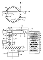
CMP加工後、膜厚をin−line計測する場合、オフラインの膜厚計測装置と異なり、膜厚計測によりCMP装置のスループットが低下しないように、in−line膜厚計測時間はできるだけ小さくする必要がある。一方、計測結果の面内膜厚分布を基に次のウェハのCMP加工条件を変更するためには、ウェハ全面にわたりある程度詳細な膜厚分布が必要になる。一般に、CMPの研磨レートはパターン密度が高い領域で遅く、密度が低い領域で速い。従って、CMP加工後の膜厚はチップ内で配線、素子の密度の違いで場所によって大きく異なり、平坦性が問題となる。又、パターン密度の分布は各チップで同一のため、ウェハ上の各チップで同一の膜厚分布となる筈であるが、ウェハの周辺ではパターンが無い、あるいはCMP加工時のウェハホルダの加圧分布によりウェハ全面にわたって膜厚が異なり、ウェハ全面に関する均一性が問題となる。通常、CMP加工後の膜厚の均一性を評価する場合、ウェハ上の中心と周辺のチップを選択し、各チップの膜厚計測用の特定パターン上で膜厚を計測し、ウェハ上の膜厚分布を求めている。この場合、ある程度詳細な膜厚分布を求めるには膜厚計測点を多くする必要がある。しかし、通常の方法では、チップの位置決め、膜厚計測用パターンの位置決めを行う必要があり、計測点を増やすと計測時間が長くなり、in−line計測に適さなくなる。
【0007】
特開平9−109023号公報では、CMP加工後のウェハを洗浄、乾燥の工程の前に膜厚計測ができるため、その結果を短時間で次のウェハのCMP加工に反映できる。膜厚計測の方法は詳しく述べられていないが、チップ、及び、計測パターンを指定し、各計測点に位置決めすることによって膜厚を計測すると考えられ、計測点数が増えると計測時間がかかると予想される。特開平9−298175号公報では、複数のセンサを1次元的に配列したモニタユニットアレイに対し、試料を回転させることによって1回転で膜厚分布を求めることができる。しかし、各センサは、膜厚の計測点領域での平均値を計測するとしており、チップ内でパターン密度の違いで膜厚が異なる等、計測領域内で膜厚が大きく変化している場合、膜厚計測に誤差のでる可能性が高くなる。又、特開平8−17768号公報では、CMP加工後、ウェハを吸着したCMP加工用のホルダを光学センサ上に移動することによって膜厚を計測できるが、特定位置の膜厚を計測するためには位置決めする必要がある。膜厚分布に関して述べられていないが、膜厚分布を求めるために計測点数を多くすると、計測時間が長くなると予想される。又、特開平10−98016号公報では、CMP加工後のウェハ面内の膜厚分布を求めるため、中心と周辺部の各チップを選択し、画像認識装置により各チップの同一箇所を選定して膜厚を計測し、面内膜厚分布を求めている。これまでと同様、計測点数を増やすと計測点数に比例して計測時間が長くなる。
【0008】
以上、上記に開示されている方法は面内膜厚分布を求めるためにチップ、及びチップ上の計測用特定パターンに位置決めする必要がある。また、1次元センサに対しウェハを回転し、位置決めしない場合でも、1次元センサの各センサの計測点での局所的な膜厚の変化は考慮されていない。通常、CMP加工により平坦化を行った後でも、パターン密度の違いによって、局所的にも膜厚分布が生じ、その変化は場合によってはウェハ全域の膜厚分布と同程度となる。
【0009】
本発明の目的は、CMP加工後、試料表面からの反射光の分光波形に基づいて、膜厚を計測し面内膜厚分布を求める際、試料上の測定個所及び、特定パターンの位置決めすることなしに膜厚分布を求める膜厚計測方法及びその装置を提供することにある。又、ウェハにおけるチップのように試料上の局所的領域でパターンの密度等による膜厚分布が生じる場合でも、試料の局所的な膜厚分布とは別に試料全面にわたる膜厚分布を求める膜厚計測方法及びその装置を提供することにある。又、半導体デバイスの製造ラインで、成膜後、表面の平坦化処理工程において、CMP加工後、試料表面からの反射光の分光波形に基づいて、膜厚を計測し面内膜厚分布を求める際、試料上の測定個所あるいは、特定パターンの位置決めすることなしに膜厚分布を求め、得られた結果より、平坦化処理工程における次の試料の加工条件を変更し、更に平坦化処理工程以降の工程の加工条件に適用することによって、薄膜デバイスを製造する方法及びその製造装置を提供することにある。
【0010】
【課題を解決するための手段】
上記目的を達成するために、本発明はCMP加工後、膜厚を計測する際、試料を移動し、移動中の試料からの反射光の分光波形を連続的に検出し、試料全面の分光波形を検出して、試料面内の膜厚分布を求める。従来、試料からの分光波形に基づいてパターン上の膜厚を計測するには10〜20μm□と比較的大きなパターンを必要とし、膜厚計測用の特定パターンに位置決めする必要があった。本発明では分光波形の検出点におけるパターンの有無とは無関係に連続的に分光波形を検出する。その際、スクライブライン等、パターンの無い部分の分光波形を検出すると分光波形から層間膜の最表面の膜厚は計測できない。しかし、試料を移動させることによって計測視野が相対的に広くなり、スクライブライン付近の分光波形を検出すると、検出視野内にパターンが存在し、パターンの面積率が30%程度以上あるとき、分光波形から膜厚が得られる。光学系により計測視野を大きくする方法もあるが、視野内で膜厚変化する割合が高くなり高精度の膜厚計測ができない。
【0011】
又、本発明は分光波形検出時、試料を移動状態で検出するため、分光波形検出点に位置決めして試料を停止する動作、及び再度位置決めするための試料を移動させる動作が必要ないため、高速に膜厚分布を得ることができる。又、計測点を増やしても、試料を移動する速度は一定のため計測時間はそれ程増加せず、比較的短時間で計測点数の多い膜厚分布を得ることができる。膜厚分布は短時間で得られるため、得られた膜厚分布を基にして、平坦化処理工程における次の試料の加工条件を設定することができる。又、比較的詳細な膜厚分布が得られるため、平坦化処理工程以降の工程の加工条件に適用することが可能となる。
【0012】
又、上記目的を達成するために、本発明はCMP加工後、膜厚を計測する際、ウェハにおけるチップのように試料上の局所的領域でパターンの密度等による膜厚分布が生じ、その膜厚分布の変化が大きく、ウェハ面全域の膜厚分布と同程度となる場合にも膜厚分布を計測可能にする。その場合、分光波形の検出方向の軌道上で検出領域を複数の矩形状の区分領域に分割し、各区分領域で分光波形を連続的に検出する。区分領域で検出した分光波形からその区分領域における膜厚分布を求め、求めた各区分領域の膜厚分布から区分領域毎に最大値、平均値等、その区分領域を代表する膜厚値を求め、得られた各区分領域の膜厚を基に試料全面の膜厚分布を求める。これにより、パターン密度の違いによる局所的な膜厚分布が大きく変化し、ウェハ面全域の膜厚分布の変化と同程度になるような場合でも、局所的な膜厚分布に依存しないウェハ全面の膜厚分布を得ることができる。
【0013】
【発明の実施の形態】
本発明の実施の形態を、図により説明する。図1は、半導体デバイスの製造ラインにおけるCMP工程において、CMP加工後、ウェハ表面の膜厚を実際のデバイスパターン上で計測し、ウェハ面内の膜厚分布を求める例を示す。
【0014】
膜厚計測装置はステージ部10、検出光学系20、光学系移動部30、膜厚計測処理部40で構成され、ここでは図示されないCMP装置に組み込まれている。ステージ部10はウェハ14を載置する回転ステージ11、回転ステ−ジ11の特定位置の通過を検出する光電センサ12、回転ステージ11を回転する駆動モータ13から構成される。CMP加工後のウェハ14表面の分光波形を検出する検出光学系20は対物レンズ21、ハーフミラー22、結像レンズ23、リレーレンズ24、空間フィルタ25、視野絞り26、照明光源27、分光器28から構成される。照明光源27はキセノンランプ又はハロゲンランプ等の白色照明光源で白色照明光をハーフミラー22、対物レンズ21を介してウェハ14に照射する。ウェハ14からの反射光は対物レンズ21、ハーフミラー22、結像レンズ23、リレーレンズ24、空間フィルタ25、視野絞り26を介して分光器28に導かれる。分光器28で分光された分光波形は電気信号として膜厚計測処理部40に入力され、膜厚を算出してウェハ面内膜厚分布を求める。光学系移動部30は光学系移動ガイド31、駆動モータ32で構成され、検出光学系20を回転ステージ11の半径方向に移動することによってウェハ全面の分光波形を検出する。膜厚計測処理部40では、光学系移動処理41で検出光学系20の半径方向の移動量制御、分光器設定処理42で試料の周速度の変化に対応した分光器読取り時間の設定を行う。分光波形検出処理43で分光波形を入力し、照明光源の分光強度特性を除去し、ウェハの反射率分光波形を得る。全周検出処理44で検出光学系20が全面検出したか否かの判定を行う。波形補正処理45では、得られた分光波形に対しウェハ表面膜下のパターンの反射率による影響等の補正を行い、分光波形の歪みをなくす。周波数・位相解析処理46では波形補正された分光波形の横軸を波長の逆数に変換し、特開2000−310512号公報で開示している方式により分光波形の周波数・位相解析を行う。膜厚算出処理47で、周波数・位相解析結果に基づいて膜厚算出を行う。膜厚算出はフィッティング処理によっても行うことができる。この場合、波形補正処理45、周波数・位相解析処理46による処理は行わない。エリア処理48ではウェハ内のチップでパターン密度の違いによって膜厚分布が生じる場合、検出する区分領域毎にその区分領域を代表する膜厚を求める処理を行う。膜厚分布表示処理49では各区分領域で求めた膜厚をもとに膜厚分布を求め、表示する。
【0015】
次にウェハ全面の分光波形を求める方法について、図2により説明する。ウェハ14は、回転ステージ11に設置される。このとき、図示されないプリアライメント部によってウェハ14の外形からウェハ14の中心位置を決め、ノッチから座標軸を一致させる。回転ステージ11を一定回転数、例えば20rpmで回転させ、膜厚分布算出終了時まで、同一回転数を保つ。膜厚計測処理部40の光学系移動処理41によって駆動モータ32を駆動し、検出光学系20を光学系移動ガイド31に沿って移動し、ウェハ14の半径方向を走査する。CMP加工後の膜厚の面内分布は様々な分布をとりうるが、例えば2図の(1)に示す膜厚分布63のように、半径上ある程度の計測点61を取らないと精度よく表せられない場合が多い。そのため、半径方向には従来例のように外周付近で1点とはせずに数個の計測点61を設定する。ウェハ14の半径方向の走査には図2の(2)〜(5)に示されるようにいくつかの方法がある。図2の(2)同心円軌道では最初の1回転で検出光学系20は静止した状態で、ウェハ14の同一円周64上における計測点61の分光波形を検出する。光電センサ12で次の回転を検出し、次の回転では分光波形の検出は行わず、光学系移動処理41によって検出光学系20を1つ内側の周軌道65に移す。このように回転ステージ11の回転を停止することなく2回転で1周分の分光波形を検出することができるため、短時間でウェハ14全面の分光波形の検出が可能である。図2の(3)螺旋軌道1では回転ステ−ジ11の1回転中に検出光学系20を円周の最外部66から最内部67に移動するもので、1回転でウェハの円周方向の分光波形を検出する。この場合、検出光学系20の移動速度を考慮して回転ステージ11の回転数を低速にしても、1回転で分光波形を検出できるため、計測時間をより短くすることができる。また、通常、CMP加工後の面内分布は半径方向には依存するが、円周方向には依存しない場合が多いため、(3)螺旋軌道1による面内膜厚分布でも有益な情報が得られる。2図の(4)螺旋軌道2では、光学系移動41によって、検出光学系20を光学系移動ガイド31上、一定速度で移動し、回転ステージ11の複数回転でウェハ全面の分光波形を検出するものである。2図の(5)直線軌道では回転ステ−ジ11を停止し、検出光学系20を移動しウェハの両端68,69間の分光波形を検出するものである。本実施形態では、ウェハ全面の分光波形を検出するため光学系を移動したが、光学系は固定し、回転するステージを一方向に移動させてもよい。
【0016】
次に図3、図4、図5、図6により、各計測点61における分光波形の検出方法を説明する。図3にウェハをCMP加工した後の膜厚分布75を示す。ウェハ上のチップ71は密なパターン72と疎なパターン73で構成されパターン上に層間絶縁膜が形成されている。ウェハのCMP加工後の線74上における膜厚は、CMP加工の研磨レートがパターン密度の高い領域で遅く、密度の低い領域で速いため、チップ71内で膜厚はパターン密度に対応した膜厚分布75となる。このような膜厚分布をもったウェハに対し、大きな視野で分光波形を検出すると、算出した膜厚は誤差が大きくなるため、検出視野は小さくする。本実施形態では検出視野は20〜50μmφ程度としたが、これに限るものでなく更に小さくしてもよい。図4に検出視野を20〜50μmφでパターン84上の層間絶縁膜85の膜厚を計測する場合を示す。パターン上の視野82で分光波形を検出すると、検出した分光波形から最表面の膜厚を計測できる。しかし、スクライブライン等、パターンの無い部分の視野81で分光波形を検出すると分光波形から層間膜の最表面の膜厚は計測できない。そこで、ウェハを移動し、移動方向の実効的な検出視野83を1mm程度と広くすることにより、検出視野内のパターンの面積率が30%程度以上になるようにして、分光波形から膜厚を算出する。こうして、移動方向の実行的な視野を大きくすることにより、ウェハ上、殆どのパターンに対して誤差なく膜厚計測できる。ところで、こうして設定した検出視野83ではチップ71上のある一部分しか膜厚が得られなくなるため、本方式では図5に示すようにウェハの移動方向に連続的に検出箇所76で分光波形を検出する。各検出箇所76の検出視野内での膜厚の変化は小さいため、膜厚は精度良く求まる。通常、ウェハ面内の膜厚分布を求めるには各チップの同一箇所の膜厚、あるいはスクライブライン上の同一形状、同一サイズのパターンの膜厚を求める。本方式ではパターンに位置決めして膜厚測定を行わないため、図6に示すように各計測点61で検出箇所76(矩形は円周方向に長いが、作図の都合上、短くなっている)が複数個のチップ71にまたがるように、検出方向に長い矩形状の区分領域77で連続的に分光波形を検出する。区分領域77で検出した分光波形から各検出箇所76の膜厚を求め、求めた膜厚から区分領域77における最大値、平均値等を求め各計測点61の膜厚とする。
【0017】
次に図7によりウェハの移動方向の実効的検出視野83(矩形は円周方向に長いが、作図の都合上、短くなっている)を検出光学系20の位置に応じて一定値に保つ方法を説明する。検出光学系20を半径方向に走査する同心円軌道、螺旋軌道方式では、回転ステージ11は一定数で回転しているため、検出箇所の回転速度96は図7(3)に示すように検出箇所の半径方向位置に比例する。そのため分光器28の読取り速度を一定値にすると図7(1)、(2)に示すように外周における検出箇所91、94に対し、内周における検出箇所92、95でのウェハ回転方向の実効的検出視野83は小さくなる。そこで分光器設定処理42において、図7(3)に示すように分光器の読取り速度97を検出箇所76の半径方向に反比例させて分光器28に設定することにより、検出光学系20の位置によらず、実効的検出視野を一定値とする。
【0018】
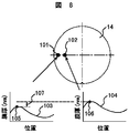
次に各計測点で計測された膜厚を基にウェハ14面内の膜厚分布を求める方法を図8により説明する。ウェハ14面上の計測点101、102では分光波形を検出箇所76で連続的に検出して膜厚分布103、104(ここでは、およそ1チップ分)を得る。CMP加工で平坦性が得られれば膜厚分布103、104はフラットになるが、通常は図8に示すように変化のある膜厚分布をもつ。そのため膜厚分布103、104から計測点101、102の膜厚を求める。膜厚分布103、104から膜厚を求める方法としては膜厚分布の最大値、最小値、平均値等を求める方法がある。ここでは、最大値105、106を使用し、それぞれ、計測点101、102における膜厚とする。膜厚差107が計測点101、102間の膜厚変化となる。ウェハ面内の各計測点についてエリア処理48で上記の処理を繰り返し、膜厚分布表示処理でウェハ面内の膜厚を表示する。
【0019】
尚、本方式ではパターンに位置決めして膜厚測定を行わないため、図6に示すように各計測点61で検出箇所76が2〜3個のチップ71にまたがるような区分領域77で連続的に分光波形を検出したが、検出光学系を20同心円軌道で走査する場合、チップの全領域をカバーできない割合が高くなる。そのため、図9に示すように各計測点111、112で半径方向の位置を僅かにずらした複数の軌道で分光波形を検出し、区分領域114で膜厚の検出箇所113を増やすことにより各計測点で精度良く膜厚を計測できるようにしても良い。又、図10に示すように計測点の軸方向121、122をウェハの軸方向123、124からずらして、チップの全領域をカバーする割合を高くしても良い。
【0020】
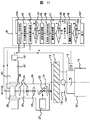
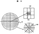
次に本発明の第2実施形態として、図11、図12により、半導体デバイスの製造ラインにおけるCMP工程において、CMP加工後、ウェハ表面の膜厚を実際のデバイスパターン上で計測し、チップ上の膜厚分布とウェハ面内の膜厚分布の両者を同一の膜厚計測装置で求める方式を示す。本実施形態の膜厚計測装置の構成は第1実施形態の膜厚計測装置の構成に対しステージ部10にX軸ステージ131、ステージ駆動モータ132が新たに加わり、膜厚計測処理部40の光学系移動処理41が光学系・ステ−ジ移動処理133、全面検出処理44が全点検出処理134に置き換わり、チップ内処理135、ウェハ面内処理136、終了処理137が新たに加わった以外、同一である。膜厚計測装置は、ここでは図示されないCMP装置に組み込まれている。本膜厚計測装置では、最初、ウェハ上、任意の1チップの膜厚分布を計測し、その後、ウェハ面内の膜厚分布を計測する。始めに、チップ内の膜厚分布を計測する方式を示す。ウェハ14は、図示されないプリアライメント部によってウェハ14の外形及び、ノッチから座標軸を一致させて回転ステージ11に設置する。チップ内の膜厚分布計測時、回転ステージ11は静止させる。始めに、光学系・ステージ移動処理133によってX軸ステージ131、検出光学系20を移動し、図12に示すように計測するチップ141の計測開始点142に検出光学系20を位置決めする。検出光学系20を静止し、X軸ステージ131を駆動し、第1実施形態の場合と同様にウェハ14の移動状態で分光波形を連続的に検出する。移動方向の実効的検出視野は500μm〜1mmで1ライン上、5〜10点分光波形を検出する。1ライン上予め決められた個数検出すると、X軸ステージ131の移動を停止し、検出光学系20を1ライン(1〜2mm)分移動する。再度、X軸ステージ131を移動して分光波形を検出し、同様の処理を繰り返しチップ全面の分光波形を検出する。ステージの送り速度は一定のため、分光器の読取り速度は全面で一定である。ステージの停止は分光波形検出点で行わず、チップ両端のみで行う。又、分光波形計測点におけるパターンの位置決めも行わないため、計測時間は短くできる。
【0021】
次に、得られた分光波形から膜厚を算出する。ウェハ移動方向における実効的検出視野は静止時に比較し大きくなるが検出視野の膜厚変化は比較的小さいため、膜厚は誤差を小さく計測できる。又、実効的検出視野が大きくなったため、視野内にパターンがない場合の割合が低くなり、膜厚計測できない割合が低くなる。チップ内の膜厚分布を計測する場合、計測した膜厚をそのままチップ内の膜厚分布として用いるためチップ内処理135でエリア処理48を行わず、膜厚分布表示処理49でチップ内膜厚分布を表示する。
【0022】
チップ内膜厚分布計測後、第1実施形態で説明した方式でウェハ14面内膜厚分布の計測点143の膜厚を計測し、ウェハ面内膜厚分布を求める。
【0023】
次に本発明の第3実施形態として、図13により、半導体デバイスの製造ラインにおけるCMP工程において、CMP加工後、ウェハ面内の膜厚分布の計測を水中で行う方式を示す。CMP加工したウェハは、通常、洗浄装置で洗浄されるまで、ウェハに付着した研磨砥粒が固着しないように水中で保管される。そこで本膜厚計測装置でも、水中で計測する。ウェハ表面の膜厚は実際のデバイスパターン上で特定パターンの位置決めを行うことなしに計測する。
【0024】
膜厚計測装置はウェハホルダ部150、検出光学系20、光学系移動部30、膜厚計測処理部40で構成され、ウェハホルダ部150以外は、配置は異なるが構成要素、処理要素は第1実施形態と同一である。膜厚計測装置は、ここでは図示されないCMP装置に組み込まれている。ウェハホルダ部150はウェハ14を保持するホルダ151、ホルダ151の特定位置の通過を検出する光電センサ152、ホルダ11を回転する駆動モータ153、膜厚計測時、ウェハを収容する水槽154、検出光学系20で分光波形を検出するガラス窓155、水槽154を満たす水156から構成される。
【0025】
次にウェハ全面の分光波形を求める方法について、図13により説明する。ウェハ14は、ノッチを検出して座標軸を決定し、ホルダ151で真空吸着によりウェハ14の表面を下にして保持する。ホルダ151を水槽154内の水156に沈め、ウェハ表面とガラス間の距離を数mm程度にする。ホルダ151を一定回転数で回転させ、膜厚分布算出終了時まで、同一回転数を保つ。膜厚計測処理部40の光学系移動処理41によって駆動モータ32を駆動し、検出光学系20を光学系移動ガイド31に沿って移動し、ウェハ14の半径方向を走査する。半径方向の走査には第1実施形態で説明したような同心円軌道、螺旋軌道があり、ウェハの回転を停止せず、分光波形を連続的に検出し、短時間でウェハ全面の分光分布を得る。分光波形検出時、ウェハの回転方向の実効的検出視野は大きくなるが、視野内での膜厚変化が小さいため、誤差なく膜厚を計測できる。また、実効的検出視野が大きくなるためパターンの無い部分で計測できない確率が低くなる。本実施形態では水156を介して分光波形を検出するが、水156の屈折率が空気の屈折率より層間絶縁膜の屈折率に近くなるため、分光波形の振幅が小さくなる。そこで、波形補正処理45で分光波形の振幅の補正を行う。
【0026】
本方式ではパターンに位置決めして膜厚測定を行わないため、第1実施形態で説明したように各計測点で検出箇所が2〜3個のチップ71にまたがるように連続的に分光波形を検出し、検出した分光波形から各検出箇所の膜厚を求め、エリア処理48で求めた膜厚の最大値、平均値等を求め各計測点の膜厚とする。各計測点の膜厚を用い、膜厚分布表示処理49でウェハ面内膜厚分布を表示する。
【0027】
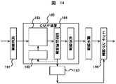
次に本発明の第4実施形態として、図14により、半導体デバイスの製造ラインで、成膜後、CMP装置162、及びその後のエッチング装置166で、プロセスを最適化する方法を示す。成膜装置161で成膜されたウェハはCMP装置162に移送される。CMP装置162ではCMP加工部163でCMP加工を行い、加工後、CMP装置に組み込まれた膜厚計測装置164においてin−lineで膜厚計測を行う。膜厚計測はウェハ上、実際のデバイスパターン上で特定のパターンに位置決めすることなく連続的に行うため、短時間にしかも比較的詳細な膜厚分布が得られる。CMP加工条件設定部165では、得られたウェハ面内膜厚分布に基づき研磨ヘッド加圧力、研磨ヘッド加圧分布、加工時間等の設定を行う。CMP加工部163はCMP加工条件設定部165の設定に従い、CMP加工を行う。ウェハ毎に、毎回同様の処理を行うことにより、ウェハの面内均一性が図れると共に、ウェハ間の膜厚均一性の向上も図れる。又、転送部167によって面内膜厚分布をCMP工程以降のエッチング装置166に転送し、エッチング装置166における加工条件の最適化のために使用する。
【0028】
次に本発明の第5実施形態として、図15により、半導体デバイスの製造ラインで、成膜装置161、及びその後のCMP装置162で、プロセスを最適化する方法を示す。成膜装置161の成膜部173で成膜されたウェハは、成膜装置に組み込まれた膜厚計測装置174においてin−lineで膜厚計測を行う。膜厚計測はCMP装置162に組み込まれた膜厚計測装置164と同様、ウェハ上の、実際のデバイスパターン上で特定のパターンに位置決めすることなく連続的に行い、短時間で比較的詳細な膜厚分布を得る。成膜条件設定部175では、得られたウェハ面内膜厚分布に基づき、ガス流量、成膜時間等の成膜条件の設定を行う。成膜部173は成膜条件設定部175の設定に従い、成膜を行う。これにより、ウェハの面内均一性が図れると共に、ウェハ間の膜厚均一性の向上も図れる。又、転送部177によって面内膜厚分布を次工程のCMP装置162のCMP加工条件設定部165に転送する。CMP加工条件設定部165では、成膜装置161から転送された面内膜厚分布と、CMP装置162でCMP加工後、膜厚計測装置164でin−line計測された膜厚分布とからCMP加工部の研磨レートを計算し、次ウェハの研磨時間の算出に用いる。
【0029】
【発明の効果】
本発明によれば、CMP加工後、ウェハの膜厚分布を求める際、ウェハ上の計測用特定パターンに位置決めすることなく、ウェハの回転状態で分光波形を連続的に検出するため、短時間で比較的多数の計測点で膜厚計測可能となり、比較的詳細なウェハ面内膜厚分布を得ることができる。又、半導体デバイスの製造ラインで、成膜後、表面の平坦化処理工程において、CMP加工後、短時間で比較的詳細なウェハ面内膜厚分布を計測できるため、次のウェハのCMP加工における加工条件に適用することにより、CMP加工工程での均一性の最適化が図れると共に、平坦化処理工程以降のエッチング工程等の加工条件にも適用でき、高精度な半導体デバイスの製造が可能となる。
【図面の簡単な説明】
【図1】本発明の第1実施形態における膜厚計測装置の装置構成を示す概略図である。
【図2】光学系を走査して、ウェハ全面の分光波形を検出する方式を説明する概略図である。
【図3】チップ内のパターン密度と膜厚の関係を説明する概略図である。
【図4】分光波形検出時、ウェハの移動により実効的検出視野を大きくする方式を説明する概略図である。
【図5】分光波形をウェハ移動方向に連続的に検出する方式を説明する概略図である。
【図6】各計測点で複数のチップにまたがるように連続的に分光波形を検出する方式を説明する概略図である。
【図7】ウェハの移動方向の実効的検出視野を光学系の位置に応じて一定値に保つ方式を説明する概略図である。
【図8】各計測点で計測された膜厚を基にウェハ全面の膜厚分布を求める方式を説明する概略図である。
【図9】各計測点で複数の軌道で分光波形を検出し、膜厚の検出箇所を増やすことにより精度良く膜厚計測する方式を説明する概略図である。
【図10】計測点の軸方向をウェハの軸方向からずらして、チップの全領域をカバーする割合を高くする方式を説明する概略図である。
【図11】本発明の第2実施形態における膜厚計測装置の装置構成を示す概略図である。
【図12】チップとウェハの面内分布を同一膜厚計測装置で計測する方式を説明する概略図である。
【図13】本発明の第3実施形態における膜厚計測装置の装置構成を示す概略図である。
【図14】本発明の第4実施形態における半導体デバイスの製造ラインでのCMP装置におけるプロセスを示す概略図である。
【図15】本発明の第5実施形態における半導体デバイスの製造ラインでの成膜装置におけるプロセスを示す概略図である。
【符号の説明】
10…ステージ部、11…回転ステージ、12…光電センサ、13…駆動モータ、14…ウェハ、20…検出光学系、21…対物レンズ、22…ハーフミラー、23…結像レンズ、24…リレーレンズ、25…空間フィルタ、26…視野絞り、27…照明光源、28…分光器、30…光学系移動部、31…光学系移動ガイド、32…駆動モータ、40…膜厚計測処理部、41…光学系移動処理、42…分光器設定処理、43…分光波形検出処理、44…全周検出処理、45…波形補正処理、46…周波数・位相解析処理、47…膜厚算出処理、48…エリア処理、49…膜厚分布表示処理、131…X軸ステージ、132…ステージ駆動モータ、133…光学系・ステ−ジ移動処理、134…全点検出処理、135…チップ内処理、136…ウェハ面内処理、137…終了処理、150…ウェハホルダ部、151…ホルダ、152…光電センサ、153…駆動モータ、154…水槽、155…ガラス窓、156…水、161…成膜装置、162…CMP装置、163…CMP加工部、164…膜厚計測装置、165…CMP加工条件設定部、166…エッチング装置、167…転送部、173…成膜部、174…膜厚計測装置、175…成膜条件設定部、177…転送部。[0001]
TECHNICAL FIELD OF THE INVENTION
The present invention relates to a method for manufacturing a semiconductor device by measuring the thickness and thickness distribution of an optically transparent film and managing the film thickness. The present invention relates to a method for measuring a surface film thickness of a wafer in a surface treatment process, and a method for manufacturing a semiconductor device by managing a planarization process by measuring the film thickness. Examples of the transparent film include, in addition to semiconductor devices such as silicon, resist films and insulating films in the process of manufacturing thin film devices such as DVDs, TFTs, and LSI reticles.
[0002]
[Prior art]
A semiconductor device is manufactured by forming elements and wiring patterns on a silicon wafer through various processes such as film formation, exposure, and etching. In recent years, in order to realize higher precision and higher density, elements and wiring patterns are moving toward miniaturization and multilayering. When a fine pattern is formed in multiple layers, the unevenness of the wafer surface increases, and it becomes difficult to accurately expose the fine pattern. Therefore, a method of flattening the wafer surface on which a protective film or an insulating film is formed after forming a multilayer wiring layer is adopted.
[0003]
As this flattening process, CMP (Chemical Mechanical Polishing) for polishing and flattening the surface by chemical and physical actions is used. CMP is a processing method known in the art.
[0004]
Important issues in the CMP process include a decrease in the accuracy of the remaining film thickness after the completion of the process due to a change in the polishing rate and a non-uniformity of the film thickness in the processed surface. Therefore, an in-line measurement technique is required that measures the film thickness after the CMP processing, changes the CMP processing conditions of the next wafer based on the measurement result, and allows the measured wafer to be subjected to the CMP processing again. . Until now, various methods have been proposed as in-line measurement techniques.
[0005]
Japanese Patent Application Laid-Open No. 9-109023 discloses an in-line measurement system capable of measuring a film thickness in water attached to an exit station of a CMP apparatus. In Japanese Patent Application Laid-Open No. 9-298175, after a CMP process is performed on a substrate holding portion during a CMP process, a plurality of sensors are moved to a monitor unit array portion in which a plurality of sensors are one-dimensionally arranged, and a sample is rotated. A method for obtaining a film thickness distribution is disclosed. Japanese Patent Application Laid-Open No. H8-17768 discloses a method in which after CMP processing, a holder holding a wafer is moved onto an optical sensor, and the wafer is irradiated with visible light to determine a film thickness. Japanese Patent Application Laid-Open No. Hei 10-98016 discloses a method in which a measuring unit is incorporated in a CMP apparatus, and after CMP processing, the film thickness is measured by a wet method.
[0006]
[Problems to be solved by the invention]
When measuring the film thickness in-line after the CMP process, unlike the offline film thickness measurement device, the in-line film thickness measurement time needs to be as short as possible so that the throughput of the CMP device does not decrease due to the film thickness measurement. is there. On the other hand, in order to change the CMP processing conditions of the next wafer based on the in-plane film thickness distribution of the measurement result, a somewhat detailed film thickness distribution is required over the entire wafer. In general, the polishing rate of CMP is low in a region where the pattern density is high, and is high in a region where the density is low. Therefore, the film thickness after the CMP processing greatly differs depending on the location in the chip due to the difference in the density of wiring and elements, and there is a problem of flatness. Since the pattern density distribution is the same for each chip, the same film thickness distribution should be obtained for each chip on the wafer. However, there is no pattern around the wafer, or the pressure distribution of the wafer holder during CMP processing. Therefore, the film thickness varies over the entire surface of the wafer, and uniformity over the entire surface of the wafer becomes a problem. Normally, when evaluating the uniformity of the film thickness after the CMP process, select the center and peripheral chips on the wafer, measure the film thickness on a specific pattern for measuring the film thickness of each chip, and measure the film thickness on the wafer. We want the thickness distribution. In this case, it is necessary to increase the number of film thickness measurement points in order to obtain a somewhat detailed film thickness distribution. However, in a usual method, it is necessary to perform positioning of a chip and positioning of a pattern for measuring a film thickness. When the number of measurement points is increased, a measurement time becomes longer, and the measurement is not suitable for in-line measurement.
[0007]
In Japanese Patent Application Laid-Open No. 9-109023, since the film thickness can be measured before the steps of cleaning and drying the wafer after the CMP processing, the result can be reflected in the CMP processing of the next wafer in a short time. Although the method of measuring the film thickness is not described in detail, it is considered that the film thickness is measured by specifying the chip and the measurement pattern and positioning at each measurement point, and it is expected that the measurement time will increase if the number of measurement points increases Is done. In Japanese Patent Application Laid-Open No. 9-298175, a film thickness distribution can be obtained in one rotation by rotating a sample in a monitor unit array in which a plurality of sensors are arranged one-dimensionally. However, each sensor measures the average value in the measurement point area of the film thickness, and when the film thickness greatly changes in the measurement area, such as a difference in film thickness due to a difference in pattern density in the chip, The likelihood of an error in the film thickness measurement increases. In Japanese Patent Application Laid-Open No. H8-17768, after the CMP processing, the film thickness can be measured by moving the CMP processing holder on which the wafer is sucked onto the optical sensor. Need to be positioned. Although there is no mention of the film thickness distribution, it is expected that the measurement time will be lengthened if the number of measurement points is increased to obtain the film thickness distribution. In Japanese Patent Application Laid-Open No. Hei 10-98016, in order to obtain the film thickness distribution in the wafer surface after the CMP processing, each chip at the center and the periphery is selected, and the same location of each chip is selected by an image recognition device. The film thickness is measured, and the in-plane film thickness distribution is obtained. As before, increasing the number of measurement points increases the measurement time in proportion to the number of measurement points.
[0008]
As described above, in the method disclosed above, it is necessary to position the chip and the measurement specific pattern on the chip in order to obtain the in-plane film thickness distribution. Further, even when the wafer is rotated with respect to the one-dimensional sensor and positioning is not performed, a local change in film thickness at a measurement point of each sensor of the one-dimensional sensor is not considered. Normally, even after flattening by CMP processing, a film thickness distribution occurs locally due to a difference in pattern density, and in some cases, the change is approximately the same as the film thickness distribution over the entire wafer.
[0009]
An object of the present invention is to measure a film thickness based on a spectral waveform of light reflected from a sample surface after a CMP process and obtain an in-plane film thickness distribution, and to position a measurement position on the sample and a specific pattern. It is an object of the present invention to provide a method and an apparatus for measuring a film thickness for obtaining a film thickness distribution without using it. Further, even when a film thickness distribution due to the pattern density or the like occurs in a local region on the sample such as a chip on a wafer, the film thickness measurement for obtaining the film thickness distribution over the entire sample separately from the local film thickness distribution of the sample. It is an object of the present invention to provide a method and an apparatus therefor. Also, in a semiconductor device manufacturing line, after film formation, in a surface flattening process, after CMP processing, the film thickness is measured based on the spectral waveform of the reflected light from the sample surface to obtain the in-plane film thickness distribution. At this time, the film thickness distribution is obtained without positioning a measurement point or a specific pattern on the sample, and from the obtained result, the processing condition of the next sample in the flattening process is changed, and further, after the flattening process, The present invention provides a method for manufacturing a thin film device and an apparatus for manufacturing the same by applying to the processing conditions of the above step.
[0010]
[Means for Solving the Problems]
In order to achieve the above object, the present invention moves the sample when measuring the film thickness after the CMP process, continuously detects the spectral waveform of the reflected light from the moving sample, and obtains the spectral waveform of the entire surface of the sample. Is detected to determine the film thickness distribution in the sample plane. Conventionally, to measure a film thickness on a pattern based on a spectral waveform from a sample, a relatively large pattern of 10 to 20 μm □ was required, and positioning to a specific pattern for film thickness measurement was required. In the present invention, a spectral waveform is continuously detected regardless of the presence or absence of a pattern at a detection point of the spectral waveform. At this time, if a spectral waveform of a portion having no pattern such as a scribe line is detected, the thickness of the outermost surface of the interlayer film cannot be measured from the spectral waveform. However, by moving the sample, the measurement visual field becomes relatively wide, and when a spectral waveform near the scribe line is detected, when the pattern exists in the detection visual field and the area ratio of the pattern is about 30% or more, the spectral waveform becomes larger. Gives the film thickness. Although there is a method of enlarging the measurement visual field by an optical system, the rate of change in the film thickness in the visual field becomes high, and high-precision film thickness measurement cannot be performed.
[0011]
In addition, since the present invention detects a sample in a moving state when detecting a spectral waveform, it does not require an operation of stopping the sample by positioning it at the spectral waveform detection point and an operation of moving the sample for re-positioning. And a film thickness distribution can be obtained. Even if the number of measurement points is increased, the measurement time does not increase so much because the moving speed of the sample is constant, and a film thickness distribution having a large number of measurement points can be obtained in a relatively short time. Since the film thickness distribution can be obtained in a short time, the processing conditions of the next sample in the flattening process can be set based on the obtained film thickness distribution. In addition, since a relatively detailed film thickness distribution can be obtained, it can be applied to the processing conditions in steps after the planarization processing step.
[0012]
In order to achieve the above object, the present invention provides a method of measuring a film thickness after a CMP process, wherein a film thickness distribution due to a pattern density or the like occurs in a local region on a sample like a chip on a wafer, Even when the change in the thickness distribution is large and is substantially the same as the film thickness distribution over the entire wafer surface, the film thickness distribution can be measured. In this case, the detection area is divided into a plurality of rectangular sections on the trajectory in the detection direction of the spectral waveform, and the spectral waveform is continuously detected in each section. The thickness distribution in each of the divided areas is obtained from the spectral waveform detected in each of the divided areas, and the maximum value, average value, etc., of the divided areas are obtained from the obtained thickness distribution of each of the divided areas. Then, a film thickness distribution over the entire surface of the sample is obtained based on the obtained film thickness of each of the divided regions. As a result, even when the local film thickness distribution changes greatly due to the difference in pattern density and becomes substantially equal to the change in the film thickness distribution over the entire wafer surface, the entire wafer surface does not depend on the local film thickness distribution. A film thickness distribution can be obtained.
[0013]
BEST MODE FOR CARRYING OUT THE INVENTION
An embodiment of the present invention will be described with reference to the drawings. FIG. 1 shows an example in which a film thickness on a wafer surface is measured on an actual device pattern after a CMP process in a CMP process in a semiconductor device manufacturing line to obtain a film thickness distribution in a wafer surface.
[0014]
The film thickness measuring device includes a stage unit 10, a detection optical system 20, an optical system moving unit 30, and a film thickness measurement processing unit 40, and is incorporated in a CMP device (not shown). The stage unit 10 includes a rotary stage 11 on which a wafer 14 is placed, a photoelectric sensor 12 for detecting passage of the rotary stage 11 at a specific position, and a drive motor 13 for rotating the rotary stage 11. A detection optical system 20 for detecting a spectral waveform on the surface of the wafer 14 after the CMP processing includes an objective lens 21, a half mirror 22, an imaging lens 23, a relay lens 24, a spatial filter 25, a field stop 26, an illumination light source 27, and a spectroscope 28. Consists of The illumination light source 27 is a white illumination light source such as a xenon lamp or a halogen lamp, and irradiates the wafer 14 with white illumination light via the half mirror 22 and the objective lens 21. The reflected light from the wafer 14 is guided to a spectroscope 28 via an objective lens 21, a half mirror 22, an imaging lens 23, a relay lens 24, a spatial filter 25, and a field stop 26. The spectral waveform separated by the spectroscope 28 is input to the film thickness measurement processing unit 40 as an electric signal, and the film thickness is calculated to obtain the film thickness distribution in the wafer surface. The optical system moving unit 30 includes an optical system moving guide 31 and a drive motor 32, and detects the spectral waveform of the entire surface of the wafer by moving the detection optical system 20 in the radial direction of the rotary stage 11. The film thickness measurement processing unit 40 controls the amount of movement of the detection optical system 20 in the radial direction in the optical system moving process 41, and sets the spectroscope reading time corresponding to the change in the peripheral speed of the sample in the spectroscope setting process. In the spectral waveform detection processing 43, a spectral waveform is input, the spectral intensity characteristic of the illumination light source is removed, and a reflectance spectral waveform of the wafer is obtained. In the entire circumference detection processing 44, it is determined whether or not the detection optical system 20 has detected the entire surface. In the waveform correction processing 45, the obtained spectral waveform is corrected for the influence of the reflectance of the pattern under the wafer surface film, and the like, and the distortion of the spectral waveform is eliminated. In the frequency / phase analysis processing 46, the horizontal axis of the spectral waveform whose waveform has been corrected is converted into the reciprocal of the wavelength, and the frequency / phase analysis of the spectral waveform is performed by the method disclosed in Japanese Patent Application Laid-Open No. 2000-310512. In the film thickness calculation processing 47, the film thickness is calculated based on the frequency / phase analysis result. The film thickness can also be calculated by a fitting process. In this case, the processing by the waveform correction processing 45 and the frequency / phase analysis processing 46 is not performed. In the area processing 48, when a film thickness distribution occurs due to a difference in pattern density between chips in a wafer, a process of calculating a film thickness representative of each of the divided regions to be detected is performed. In the film thickness distribution display processing 49, a film thickness distribution is obtained and displayed based on the film thickness obtained in each of the divided areas.
[0015]
Next, a method for obtaining the spectral waveform of the entire surface of the wafer will be described with reference to FIG. The wafer 14 is set on the rotating stage 11. At this time, the center position of the wafer 14 is determined based on the outer shape of the wafer 14 by a pre-alignment unit (not shown), and the coordinate axes are matched from the notch. The rotation stage 11 is rotated at a constant rotation speed, for example, 20 rpm, and the same rotation speed is maintained until the film thickness distribution calculation is completed. The drive motor 32 is driven by the optical system movement processing 41 of the film thickness measurement processing unit 40 to move the detection optical system 20 along the optical system movement guide 31 and scan the wafer 14 in the radial direction. The in-plane distribution of the film thickness after the CMP processing can take various distributions. For example, as shown in a film thickness distribution 63 shown in FIG. Often not. Therefore, several measurement points 61 are set in the radial direction instead of one point near the outer periphery as in the conventional example. There are several methods for scanning the wafer 14 in the radial direction, as shown in FIGS. In the (2) concentric orbit of FIG. 2, the detection optical system 20 is stationary at the first rotation, and the spectral waveform of the measurement point 61 on the same circumference 64 of the wafer 14 is detected. The next rotation is detected by the photoelectric sensor 12, and no spectral waveform is detected in the next rotation, and the detection optical system 20 is moved to the inner peripheral orbit 65 by the optical system moving process 41. As described above, since the spectral waveform for one round can be detected by two rotations without stopping the rotation of the rotary stage 11, the spectral waveform of the entire surface of the wafer 14 can be detected in a short time. In (3) spiral orbit 1 of FIG. 2, the detection optical system 20 moves from the outermost portion 66 to the innermost portion 67 of the circumference during one rotation of the rotation stage 11, and one rotation makes the rotation in the circumferential direction of the wafer. Detect the spectral waveform. In this case, even if the rotation speed of the rotation stage 11 is reduced in consideration of the moving speed of the detection optical system 20, the spectral waveform can be detected by one rotation, so that the measurement time can be further shortened. Usually, the in-plane distribution after the CMP processing depends on the radial direction but does not depend on the circumferential direction in many cases. Therefore, (3) useful information can be obtained even in the in-plane film thickness distribution by the spiral orbit 1. Can be In (4) spiral orbit 2 in FIG. 2, the detection optical system 20 is moved at a constant speed on the optical system movement guide 31 by the optical system movement 41, and the spectral waveform of the entire surface of the wafer is detected by a plurality of rotations of the rotary stage 11. Things. In (5) linear orbit of FIG. 2, the rotation stage 11 is stopped, the detection optical system 20 is moved, and the spectral waveform between both ends 68 and 69 of the wafer is detected. In this embodiment, the optical system is moved to detect the spectral waveform of the entire surface of the wafer. However, the optical system may be fixed, and the rotating stage may be moved in one direction.
[0016]
Next, a method of detecting a spectral waveform at each measurement point 61 will be described with reference to FIGS. 3, 4, 5, and 6. FIG. FIG. 3 shows a film thickness distribution 75 after the wafer is subjected to the CMP processing. The chip 71 on the wafer is composed of a dense pattern 72 and a sparse pattern 73, and an interlayer insulating film is formed on the pattern. The film thickness on the line 74 after the CMP process of the wafer is thinner in the chip 71 because the polishing rate of the CMP process is slower in a region with a higher pattern density and faster in a region with a lower density. A distribution 75 results. If a spectral waveform is detected in a large field of view with respect to a wafer having such a film thickness distribution, the calculated film thickness has a large error, so that the detected field of view is reduced. In the present embodiment, the detection visual field is set to about 20 to 50 μmφ, but is not limited to this and may be further reduced. FIG. 4 shows a case where the film thickness of the interlayer insulating film 85 on the pattern 84 is measured with a detection visual field of 20 to 50 μmφ. When the spectral waveform is detected in the visual field 82 on the pattern, the film thickness on the outermost surface can be measured from the detected spectral waveform. However, if a spectral waveform is detected in the field of view 81 of a part without a pattern such as a scribe line, the thickness of the outermost surface of the interlayer film cannot be measured from the spectral waveform. Then, the wafer is moved and the effective detection field 83 in the moving direction is widened to about 1 mm so that the area ratio of the pattern in the detection field becomes about 30% or more, and the film thickness is determined from the spectral waveform. calculate. In this way, by increasing the effective visual field in the moving direction, it is possible to measure the film thickness of most patterns on the wafer without errors. By the way, in the detection field 83 set in this way, only a certain part of the film thickness on the chip 71 can be obtained. Therefore, in this method, the spectral waveform is continuously detected at the detection point 76 in the moving direction of the wafer as shown in FIG. . Since the change of the film thickness in the detection field of each detection portion 76 is small, the film thickness can be determined with high accuracy. Usually, in order to obtain the film thickness distribution in the wafer surface, the film thickness of the same location of each chip or the pattern of the same shape and the same size on the scribe line is obtained. In this method, since the film thickness is not measured by positioning the pattern, the detection point 76 is detected at each measurement point 61 as shown in FIG. 6 (the rectangle is longer in the circumferential direction, but shorter for convenience of drawing). Is continuously detected in the rectangular sectioned region 77 long in the detection direction so as to extend over a plurality of chips 71. The film thickness at each detection point 76 is obtained from the spectral waveform detected in the divided area 77, and the maximum value, average value, and the like in the divided area 77 are obtained from the obtained film thickness, and are set as the film thickness at each measurement point 61.
[0017]
Next, referring to FIG. 7, a method of keeping the effective detection field of view 83 in the moving direction of the wafer (the rectangle is longer in the circumferential direction but shorter for convenience of drawing) at a constant value according to the position of the detection optical system 20. Will be described. In the concentric trajectory or spiral trajectory scanning the detection optical system 20 in the radial direction, the rotating stage 11 is rotating at a fixed number, and the rotation speed 96 of the detection point is, as shown in FIG. It is proportional to the radial position. Therefore, when the reading speed of the spectroscope 28 is set to a constant value, as shown in FIGS. 7 (1) and 7 (2), the effective position in the wafer rotation direction at the detection points 92 and 95 on the inner circumference is smaller than the detection points 91 and 94 on the outer circumference. The target detection field 83 becomes smaller. In the spectroscope setting process 42, the reading speed 97 of the spectroscope is set in the spectroscope 28 in inverse proportion to the radial direction of the detection point 76 as shown in FIG. Regardless, the effective detection visual field is set to a constant value.
[0018]
Next, a method of obtaining a film thickness distribution in the surface of the wafer 14 based on the film thickness measured at each measurement point will be described with reference to FIG. At the measurement points 101 and 102 on the surface of the wafer 14, spectral waveforms are continuously detected at the detection points 76 to obtain film thickness distributions 103 and 104 (here, about one chip). If flatness is obtained by the CMP process, the film thickness distributions 103 and 104 become flat, but usually have a variable film thickness distribution as shown in FIG. Therefore, the film thickness at the measurement points 101 and 102 is obtained from the film thickness distributions 103 and 104. As a method of obtaining the film thickness from the film thickness distributions 103 and 104, there is a method of obtaining a maximum value, a minimum value, an average value, and the like of the film thickness distribution. Here, the maximum values 105 and 106 are used, and the film thicknesses at the measurement points 101 and 102 are used, respectively. The film thickness difference 107 is a film thickness change between the measurement points 101 and 102. The above processing is repeated in the area processing 48 for each measurement point in the wafer plane, and the film thickness in the wafer plane is displayed by the film thickness distribution display processing.
[0019]
In this method, since the film thickness is not measured by positioning in a pattern, as shown in FIG. 6, a continuous area 77 is continuously formed in a divided area 77 in which a detection point 76 extends over two or three chips 71 at each measurement point 61. However, when the detection optical system is scanned in 20 concentric trajectories, the rate at which the entire area of the chip cannot be covered increases. Therefore, as shown in FIG. 9, each measurement point 111 and 112 detects a spectral waveform in a plurality of orbits whose positions in the radial direction are slightly shifted, and increases the number of locations 113 where the film thickness is detected in the divided area 114 to thereby perform each measurement. In this case, the film thickness may be measured with high accuracy. Further, as shown in FIG. 10, the axial direction 121, 122 of the measurement point may be shifted from the axial direction 123, 124 of the wafer to increase the ratio of covering the entire area of the chip.
[0020]
Next, as a second embodiment of the present invention, referring to FIG. 11 and FIG. 12, in a CMP process in a semiconductor device manufacturing line, after CMP processing, a film thickness on a wafer surface is measured on an actual device pattern, and A method is shown in which both the film thickness distribution and the film thickness distribution in the wafer surface are obtained by the same film thickness measuring device. The configuration of the film thickness measuring apparatus of the present embodiment is different from the configuration of the film thickness measuring apparatus of the first embodiment in that an X-axis stage 131 and a stage drive motor 132 are newly added to the stage unit 10, The same except that the system moving process 41 is replaced by the optical system / stage moving process 133, the whole surface detecting process 44 is replaced by the all point detecting process 134, and the in-chip process 135, the in-wafer process 136, and the end process 137 are newly added. It is. The film thickness measuring device is incorporated in a CMP device (not shown). In the present film thickness measuring apparatus, first, the film thickness distribution of an arbitrary chip on the wafer is measured, and thereafter, the film thickness distribution in the wafer surface is measured. First, a method of measuring a film thickness distribution in a chip will be described. The wafer 14 is mounted on the rotary stage 11 by using a pre-alignment unit (not shown) so that the outer shape of the wafer 14 and the coordinate axes match from the notch. When measuring the film thickness distribution in the chip, the rotating stage 11 is kept stationary. First, the X-axis stage 131 and the detection optical system 20 are moved by the optical system / stage movement processing 133, and the detection optical system 20 is positioned at the measurement start point 142 of the chip 141 to be measured as shown in FIG. The detection optical system 20 is stopped, the X-axis stage 131 is driven, and the spectral waveform is continuously detected while the wafer 14 is moving, as in the first embodiment. The effective detection visual field in the moving direction is 500 μm to 1 mm, and detects 5 to 10 spectral waveforms on one line. When a predetermined number is detected on one line, the movement of the X-axis stage 131 is stopped, and the detection optical system 20 is moved by one line (1-2 mm). The X-axis stage 131 is moved again to detect a spectral waveform, and the same processing is repeated to detect a spectral waveform on the entire surface of the chip. Since the stage feed speed is constant, the reading speed of the spectroscope is constant over the entire surface. The stop of the stage is not performed at the spectral waveform detection point, but only at both ends of the chip. In addition, since the positioning of the pattern at the spectral waveform measurement point is not performed, the measurement time can be shortened.
[0021]
Next, the film thickness is calculated from the obtained spectral waveform. Although the effective detection field of view in the wafer movement direction is larger than at rest, the change in the thickness of the detection field of view is relatively small, so that the thickness can be measured with a small error. In addition, since the effective detection visual field has become large, the ratio when there is no pattern in the visual field becomes low, and the ratio where the film thickness cannot be measured becomes low. When measuring the film thickness distribution in the chip, the measured film thickness is used as it is as the film thickness distribution in the chip. Is displayed.
[0022]
After measuring the film thickness distribution in the chip, the film thickness at the measurement point 143 of the film thickness distribution in the wafer 14 is measured by the method described in the first embodiment to obtain the film thickness distribution in the wafer.
[0023]
Next, as a third embodiment of the present invention, FIG. 13 shows a method of measuring a film thickness distribution in a wafer surface in water in a CMP process in a semiconductor device manufacturing line after CMP processing. The wafer that has been subjected to CMP processing is usually stored in water until it is cleaned by a cleaning device so that abrasive grains attached to the wafer do not adhere. Therefore, the film thickness is also measured in water by the present film thickness measuring apparatus. The film thickness on the wafer surface is measured without positioning a specific pattern on an actual device pattern.
[0024]
The film thickness measuring apparatus includes a wafer holder unit 150, a detection optical system 20, an optical system moving unit 30, and a film thickness measurement processing unit 40. Except for the wafer holder unit 150, the components and processing elements are different from those of the first embodiment. Is the same as The film thickness measuring device is incorporated in a CMP device (not shown). The wafer holder unit 150 includes a holder 151 for holding the wafer 14, a photoelectric sensor 152 for detecting passage of the holder 151 at a specific position, a drive motor 153 for rotating the holder 11, a water tank 154 for accommodating the wafer when measuring the film thickness, and a detection optical system. A glass window 155 for detecting a spectral waveform at 20 and water 156 filling a water tank 154.
[0025]
Next, a method of obtaining the spectral waveform of the entire surface of the wafer will be described with reference to FIG. The notch is detected to determine the coordinate axis, and the wafer is held by the holder 151 with the surface of the wafer 14 facing down by vacuum suction. The holder 151 is immersed in the water 156 in the water tank 154, and the distance between the wafer surface and the glass is reduced to about several mm. The holder 151 is rotated at a constant rotation speed, and the same rotation speed is maintained until the calculation of the film thickness distribution is completed. The drive motor 32 is driven by the optical system movement processing 41 of the film thickness measurement processing unit 40 to move the detection optical system 20 along the optical system movement guide 31 and scan the wafer 14 in the radial direction. The scanning in the radial direction includes the concentric orbit and the spiral orbit as described in the first embodiment. The rotation of the wafer is not stopped, the spectral waveform is continuously detected, and the spectral distribution over the entire surface of the wafer is obtained in a short time. . At the time of spectral waveform detection, the effective detection visual field in the rotation direction of the wafer becomes large, but the film thickness can be measured without error because the film thickness change within the visual field is small. In addition, since the effective detection field of view becomes large, the probability that measurement cannot be performed in a portion having no pattern is reduced. In the present embodiment, the spectral waveform is detected via the water 156. However, since the refractive index of the water 156 is closer to the refractive index of the interlayer insulating film than the refractive index of air, the amplitude of the spectral waveform is reduced. Therefore, the amplitude of the spectral waveform is corrected in the waveform correction processing 45.
[0026]
In this method, since the film thickness is not measured by positioning to the pattern, as described in the first embodiment, the spectral waveform is continuously detected at each measurement point so that the detection point extends over two or three chips 71. Then, the film thickness at each detection point is obtained from the detected spectral waveform, and the maximum value, average value, and the like of the film thickness obtained by the area processing 48 are obtained and set as the film thickness at each measurement point. Using the film thickness at each measurement point, the film thickness distribution in the wafer surface is displayed in the film thickness distribution display processing 49.
[0027]
Next, as a fourth embodiment of the present invention, a method of optimizing a process in a CMP device 162 and a subsequent etching device 166 in a semiconductor device manufacturing line after film formation is described with reference to FIG. The wafer formed by the film forming device 161 is transferred to the CMP device 162. In the CMP apparatus 162, the CMP processing is performed by the CMP processing section 163, and after the processing, the film thickness is measured in-line by the film thickness measuring apparatus 164 incorporated in the CMP apparatus. Since the film thickness measurement is continuously performed without positioning a specific pattern on a wafer or an actual device pattern, a relatively detailed film thickness distribution can be obtained in a short time. The CMP processing condition setting unit 165 sets a polishing head pressing force, a polishing head pressure distribution, a processing time, and the like based on the obtained wafer in-plane film thickness distribution. The CMP processing unit 163 performs the CMP processing according to the settings of the CMP processing condition setting unit 165. By performing the same processing for each wafer, the in-plane uniformity of the wafer can be achieved, and the uniformity of the film thickness between the wafers can be improved. The transfer unit 167 transfers the in-plane film thickness distribution to the etching apparatus 166 after the CMP process, and uses the distribution to optimize the processing conditions in the etching apparatus 166.
[0028]
Next, as a fifth embodiment of the present invention, a method of optimizing a process in a film forming apparatus 161 and a subsequent CMP apparatus 162 in a semiconductor device manufacturing line will be described with reference to FIG. The thickness of the wafer formed by the film forming unit 173 of the film forming apparatus 161 is measured in-line by a film thickness measuring device 174 incorporated in the film forming apparatus. Similar to the film thickness measuring device 164 incorporated in the CMP device 162, the film thickness measurement is continuously performed without positioning a specific pattern on an actual device pattern on a wafer, and a relatively detailed film is formed in a short time. Obtain the thickness distribution. The film forming condition setting unit 175 sets film forming conditions such as a gas flow rate and a film forming time based on the obtained film thickness distribution in the wafer surface. The film forming unit 173 forms a film according to the setting of the film forming condition setting unit 175. Thereby, the in-plane uniformity of the wafer can be achieved, and the uniformity of the film thickness between the wafers can be improved. The transfer unit 177 transfers the in-plane film thickness distribution to the CMP processing condition setting unit 165 of the CMP apparatus 162 in the next step. The CMP processing condition setting unit 165 performs the CMP processing based on the in-plane film thickness distribution transferred from the film forming apparatus 161 and the film thickness distribution measured in-line by the film thickness measuring apparatus 164 after the CMP processing by the CMP apparatus 162. The polishing rate of the portion is calculated and used for calculating the polishing time of the next wafer.
[0029]
【The invention's effect】
According to the present invention, when obtaining the film thickness distribution of the wafer after the CMP process, the spectral waveform is continuously detected in the rotating state of the wafer without positioning the specific pattern for measurement on the wafer. The film thickness can be measured at a relatively large number of measurement points, and a relatively detailed film thickness distribution within the wafer surface can be obtained. Also, in a semiconductor device manufacturing line, a relatively detailed film thickness distribution in a wafer surface can be measured in a short time after a CMP process in a surface flattening process after film formation in a semiconductor device manufacturing line. By applying to processing conditions, it is possible to optimize uniformity in the CMP processing step, and also applicable to processing conditions such as an etching step after the planarization processing step, and to manufacture a highly accurate semiconductor device. .
[Brief description of the drawings]
FIG. 1 is a schematic diagram illustrating an apparatus configuration of a film thickness measuring apparatus according to a first embodiment of the present invention.
FIG. 2 is a schematic diagram illustrating a method of scanning an optical system to detect a spectral waveform on the entire surface of a wafer.
FIG. 3 is a schematic diagram illustrating a relationship between a pattern density and a film thickness in a chip.
FIG. 4 is a schematic diagram for explaining a method of enlarging an effective detection visual field by moving a wafer during spectral waveform detection.
FIG. 5 is a schematic diagram illustrating a method for continuously detecting a spectral waveform in a wafer moving direction.
FIG. 6 is a schematic diagram illustrating a method of continuously detecting a spectral waveform so as to extend over a plurality of chips at each measurement point.
FIG. 7 is a schematic diagram illustrating a method for maintaining an effective detection field of view in a moving direction of a wafer at a constant value according to the position of an optical system.
FIG. 8 is a schematic diagram illustrating a method for obtaining a film thickness distribution over the entire surface of the wafer based on the film thickness measured at each measurement point.
FIG. 9 is a schematic diagram for explaining a method of detecting a spectral waveform at a plurality of orbits at each measurement point and accurately measuring the film thickness by increasing the number of locations where the film thickness is detected.
FIG. 10 is a schematic diagram illustrating a method of shifting the axial direction of a measurement point from the axial direction of a wafer to increase the ratio of covering the entire area of a chip.
FIG. 11 is a schematic diagram illustrating a device configuration of a film thickness measuring device according to a second embodiment of the present invention.
FIG. 12 is a schematic diagram illustrating a method of measuring the in-plane distribution of a chip and a wafer with the same film thickness measuring device.
FIG. 13 is a schematic diagram illustrating a device configuration of a film thickness measuring device according to a third embodiment of the present invention.
FIG. 14 is a schematic view showing a process in a CMP apparatus in a semiconductor device manufacturing line according to a fourth embodiment of the present invention.
FIG. 15 is a schematic view illustrating a process in a film forming apparatus in a semiconductor device manufacturing line according to a fifth embodiment of the present invention.
[Explanation of symbols]
DESCRIPTION OF SYMBOLS 10 ... Stage part, 11 ... Rotation stage, 12 ... Photoelectric sensor, 13 ... Drive motor, 14 ... Wafer, 20 ... Detection optical system, 21 ... Objective lens, 22 ... Half mirror, 23 ... Imaging lens, 24 ... Relay lens , 25 spatial filter, 26 field stop, 27 illumination light source, 28 spectroscope, 30 optical system moving unit, 31 optical system moving guide, 32 drive motor, 40 film thickness measurement processing unit, 41 Optical system movement processing, 42: spectroscope setting processing, 43: spectral waveform detection processing, 44: full circumference detection processing, 45: waveform correction processing, 46: frequency / phase analysis processing, 47: film thickness calculation processing, 48: area Processing, 49: thickness distribution display processing, 131: X-axis stage, 132: stage drive motor, 133: optical system / stage movement processing, 134: all point detection processing, 135: in-chip processing, 136 ... In-plane processing, 137 end processing, 150 wafer holder, 151 holder, 152 photoelectric sensor, 153 drive motor, 154 water tank, 155 glass window, 156 water, 161 film forming apparatus, 162 ... CMP apparatus, 163 ... CMP processing section, 164 ... Film thickness measuring apparatus, 165 ... CMP processing condition setting section, 166 ... Etching apparatus, 167 ... Transfer section, 173 ... Film forming section, 174 ... Film thickness measuring apparatus, 175 ... Film formation condition setting unit, 177 ... Transfer unit.